Source: (Popular Electronics Electronic Experimenter's Handbook (1982)
How to choose components with tolerances to insure that circuits work properly.
BY STEVEN L. CHEAIRS
ONE CONSTANTLY recurring problem for many hobbyists is that some circuits in the projects they build fail to work properly. Other than improper assembly and bad components, the most probable cause of this problem is that a "typical" circuit design was used.
A typical circuit design might be sound on paper, but unless component characteristic variations are taken into account, the design may not produce a working circuit. And the cause is normal component parameter variations. It is important, therefore, that when you design or build a project, you take into account the possible variation range of the components you will be using to ensure that the project works properly.
In this article, we will discuss why component characteristics vary and what can be done to circumvent possible problems. Stated differently, we will discuss how to design for worst-case conditions.
Why They Vary. Component characteristics can vary for any number of reasons. For example, IC's are manufactured in "batch" lots, wherein a number of identical chips are fabricated simultaneously on a single silicon wafer. This approach results in significant manufacturing savings and a very low cost per circuit element. Unfortunately, the parameters of the individual components can vary greatly from one wafer to the next, even though component characteristics on a single wafer will "track" very closely.
It is not uncommon to find a circuit that contains components whose parameters fall anywhere between their worst--case limits. If the circuit was designed around devices that have typical parameters, there is the possibility that it will not function because it contains a device that operates at an extreme end of its parameters. Here is an example.
Assume a circuit has 50 components.
Of these, 80% have typical parameters and 10% are sensitive to parameter variations. That means 20%, or 10 components, have atypical characteristics and 5 components are parameter sensitive.
The probability of an event occurring can be defined by the equation P = M/N, where P is the probability, M is the number of times the event is expected to occur, and N is the number of trials.
Hence, the probability of a sensitive component occurring per circuit is 1/10, while the probability of a component having atypical performance is 1/5.
By the Law of Multiplication Probability (compound probability), when an event is regarded as occurring if a number of sub-events independently occurs, the compound probability of occurrence of the event is equal to the product of the individual probabilities of the sub-events.
This can be expressed in a mathematical way by the equation P = P1 x P2 or P = (M1 /N1) (M2/N2). Therefore, 1/5 times 1/10 or one out of every 50 circuits may not function due to the typical design technique used in our example.
In all likelihood, the figures used in the example are applicable to many hobbyist-built projects and account for the occasional project that fails to work even when all the wiring is correct. It should also be noted that this condition is worsened when "surplus" components are used, since the probability of using a component that is just barely within its specifications increases. Using such components, it becomes possible for a designer to produce a working design prototype that when duplicated by others will fail to operate.
Given the above conditions, it becomes mandatory for all circuit designs to be subjected to worst-case design analysis if the circuit is to be duplicated by others. Any circuit can be so analyzed. The most convenient method is to use worst-case parameter values during the initial design phase to insure proper operation from the start.
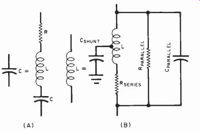
Fig.
1. A theoretical capacitor (A) actually contains parasitic R and L. Theoretical
equivalent of an inductor (B) is even more complex.
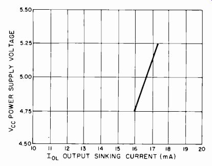
Fig. 2. Maximum sinking current as a function of power supply voltage variation.
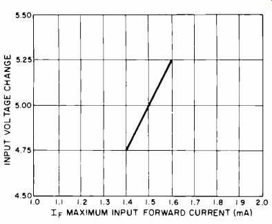
Fig. 3. Maximum input forward current as a function of the input voltage.
Defining the Problem. It is essential to recognize which parameter or combination of parameters create the worst case for a particular circuit. Unfortunately, these conditions and how they affect circuit performance vary from circuit to circuit. Also, there may be different performance specs for any given circuit.
Most modern circuits contain both IC's and discrete components. When an IC and a number of discrete components can be combined to make a subcircuit, it is acceptable and may even be desirable to consider the subcircuit thus formed as a self-contained entity. This is also true for combining gates and other elements of IC's. When circuit elements are so combined, a block diagram is created. The self-contained entities can then be individually analyzed and the results combined to analyze total circuit performance. This approach also allows system partitioning and interconnection methods to be considered, as well as such problems as impedance matching, level shifting, and fan-out.
The entire circuit's specifications can be divided down to the individual blocks that are sufficiently detailed to be treated on a stand-alone basis. All characteristics must be considered. If the circuit block does not satisfy the detailed requirements (input and output impedance, temperature range, threshold levels, propagation delay, hold times, etc.), the circuit must be modified.
Every component in a circuit must be allowed to vary over its full range of values, as specified by its tolerance, and still allow satisfactory circuit operation. It is the tolerance range that specifies the worst-case parameter range.
Every component contains parasitic components, such as capacitance, inductance, and resistance. In many circuits, the parasitic components are observed only during worst-case conditions. For example, consider a capacitor. A capacitor cannot simply be added to a high-frequency circuit with the expectation that the circuit will behave as if a theoretically pure capacitor were added. This simple component is actually quite complex, as can be seen in Fig. 1A. An inductor is even more complex, as shown in Fig. 1B. Therefore, for proper worst-case operation, these parasitic effects must be considered when designing and building circuits.
Fixed resistors also have broad tolerance specifications that can range up to ± 10% (±20% in older resistors) of their specified nominal values.
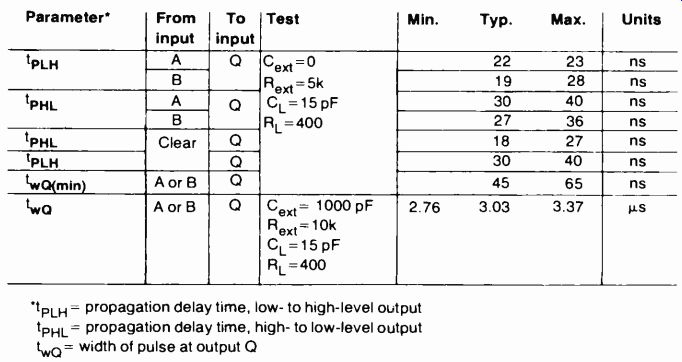
TABLE I-SWITCHING CHARACTERISTICS
Vcc=5 V, TA-25°C
'tPLH = propagation delay time, low- to high-level ot,, put tPHL = propagation delay time, high-to-low-level output two= width of pulse at output Q
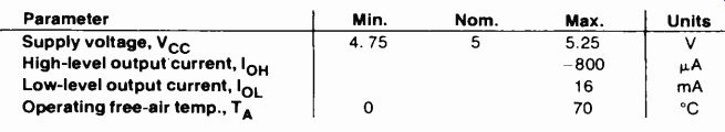
TABLE II--RECOMMENDED OPERATING CONDITIONS

TABLE III--ABSOLUTE MAXIMUM RATING OVER FREE-AIR TEMPERATURE RATING. Voltage
values are with respect to network ground terminal.
The Spec Sheet. Manufacturer specification sheets for a particular IC should be consulted for pinout and to gain a working knowledge of the device itself. A typical spec sheet, this one for a 74123 dual re-triggerable monostable multi-vibrator IC, is shown in Table I. Assume you require a 50-ns pulse and decide to use the 74123 to generate it. Note in the table that twQ(min) (minimum output pulse width) has a typical value of 45 ns and a worst-case value of 65 ns when external capacitance Cext is zero and external resistance R_ext is 5000 ohms. (If you were making only one circuit, you could hand-select the components to make it work, but this is not a safe approach to use in a construction article.) Now note two when C_est is 1000 pF and R_est is 10,000 ohms.
The width of the pulse can be between 2.76 and 3.37 µs. Hence, the value can range from +8.9% to 11.2% of the typical specified value for the given R and C values. Note also that the spec sheet does not tell you that this error is linear throughout the two range. For all we know, this may be the best point on the curve. So, when designing such a circuit, make certain that your design can accommodate this type of tolerance.
Note the column in Table II headed Nom (nominal). This value is the one for which you should strive, but you may find that it is not possible to obtain or hold it through the design.
It should be understood that one parameter may affect another. For example, consider the effect of varying the power supply voltage on the output sinking current (I_L). The output sinking current is a linear function of the power supply voltage, as shown in Fig. 2.
When the supply potential is 4.75 volts, 'the output can sink 15 mA. A similar condition can be observed in Fig 3, where the maximum input forward current (I_F) is shown as a function of input voltage. Here again, the variation of one parameter can affect another.
At this point, you should realize that you must know which characteristics are important so that you can design with a knowledge of their probable variations. To do this, you must know just what will affect a given parameter.
All of the parameters thus far discussed have been of the type that can cause circuit failure, not failure of a component. Most IC data sheets carry a set of catastrophic characteristics, such as those listed in Table Ill. With resistors and capacitors, characteristics like maximum power dissipation and breakdown voltage should never be exceeded.
Summing Up. If you use the techniques detailed in this article, or keep them in mind, your circuits will work and so will other circuits built from your design. If you build projects from magazines, steer clear of broad-tolerance components, especially in critical components.