Source: Popular Electronics--Electronic Experimenter's Handbook (1983)
BY HAROLD KINLEY
How a PLL circuit works, how M is used in communication equipment, and how to locals circuit defects
THE phase-locked-loop (PLL) cui: has been around for many years now. It wasn't until it was introduced in integrated circuit form to 40-channel CB transceiver, however, that it truly came into prominence. Now it's conspicuously used in other electronic equipment, such as FM tuners and amateur radio gear.
Presented here is detailed information on how a PLL circuit works in CB applications, followed by step-by-step troubleshooting analysis of a typical PLL CB system. The Principles are applicable to other equipment using PLLs.
Why Use PLLs?
The switch to PLLs was necessitated by the CB move from 23 to 43 channels The old system, in which a bank of crystals in a “Crystal-plexer" arrangement was used would have been prohibitively expensive. 3y sv< aching to tie PLL, .t was possible to synthesize all channel freqs es w-_th _liar_ two or Wee Increased ac curacy and stsbi_ity iv-me bonuses.
Another advantage the PLL s tl-at is digital circuitry is compat 3k w th electronic numeric displays, which provide large, easy-to-real numerals.
Actual PLL Circuit. Shown in Fig. 1 is an actual circuit commonly used in many CB transceivers. The one shown here appears in the Boman Model CB-930 transceiver. The total system, including delta-tune and transmit-stop circuits, is composed of five transistors and three integrated circuits. The small boxes in Fig. 1 are used to indicate inter connections to other circuits within the overall system.
Divider IC1 can be programmed to divide the input frequency present at pin 2 by a divisor selected via CHANNEL SELECTOR switch Si This switch provides either 5.36 volts (logic 1) or zero volts (logic 0) to programming pins 9 through 15 of IC1.
Each programming pin, has a "weight" (value) that increases in binary fashion (each number is twice the previous one) as the pin numbers go down. For example, pin 15 is weighted 1, pin 14 is 2, pin 13 is 4, etc., proceeding down to pin 7 weighted 256. Since pin 7 is permanently connected to 5.45 volts, it is always a 1 hence 256 must be added to the divisor. Pin 8 (which should be 128) is permanently connected to ground, hence it has no weight and can be disregarded.
As shown in Table I, the truth table for the IC1 programming pins, each channel has a unique array of 1's and 0's. In the case of channel 1, pins 9, 12 and 14 are selected high (1). Therefore, the divisor is 256 (pin 7) + 64 (pin 9) + 8 (pin 12) + 2 (pin 14) which equals 330, the divisor for channel 1.
Also contained in IC1 is a phase comparator and a constant divider, the latter dividing the input at pin 3 by 1024. Both inputs of the phase comparator are fed with separate 10-kHz signals and the comparator's output frequency is deter mined by the relative frequency or phase differences between the two input signals. This output is then filtered to obtain a steady dc-level "error" signal that is used to control a voltage-controlled oscillator (vco).
Vco and Mixer. Contained in IC2 are a vco and a mixer. When two different frequencies are fed to pins 2 and 4, their sum and difference appear at pins 6 and 9, respectively.
The heart of the vco is Varactor diode D1, whose capacitance varies with changes in bias voltage. The oscillator in IC2 is controlled by the external components connected to pin 1. The LC net work that parallels DI also has an effect on the nominal 17-MHz operating frequency of the vco.
Although IC2 and IC3 are identical, the oscillator in IC3 is crystal controlled at 10.695 MHz. The outputs from pin 6 of IC2 and the 10.695-MHz oscillator go to IC3's mixer. Their difference appears at pin 9 of IC3.
The basic reference frequency is generated by oscillator Q1, which operates at 10.240 MHz. The secondary of TI is tuned to the 20.480-MHz second harmonic of the oscillator signal.
Detailed Analysis. Let us use channel 1 (throughout this article) to analyze system operation. Refer to both Fig. 1 and Table I. Since pin 7 (not listed) is always high, its weight of 256 must be added to the final tally to obtain the divisor on all channels.
Also shown in the chart is the divider input at TP3 (3.300 MHz for channel 1) and the receiver and transmitter outputs at TP4.
The 3.300-MHz signal is obtained as follows. The IC2 mixer is fed a 20.480-MHz signal from T1 and another signal from the vco. The latter goes to the mixer at pin 2. The 20.480-MHz signal goes into the mixer via pin 4. The sum and difference of the two signals appear at pins 6 and 9, respectively, of IC2.
Calculate the vco frequency as follows. From Table I, the IC2 sum output frequency is 37.660 MHz. Since the vco frequency is mixed with 20.480 MHz to obtain 37.660 MHz, = 37.660 MHz- 20.480 MHz = 17.180 MHz.
The difference of the vco frequency and 20.480 MHz is 3.300 MHz, which is present at pin 9 of IC2 and pin 2 of IC1.
The programmable divider then divides the input by 330 to yield 10 kHz. This 10-kHz signal is fed, within IC1, to one of the inputs to the phase comparator.
The other 10-kHz signal used for the reference is derived as follows. A 10.240-MHz signal from the emitter of Q1 is amplified by Q2 and fed to pin 3 of IC1, where it is divided by 1024. This yields the 10-kHz reference signal required for the reference input to the phase comparator.
The comparator constantly compares the phases of the two 10-kHz signals fed to it, and its output varies with the differences. Since the reference oscillator is crystal controlled, its output is very stable. The frequency of the signal from the vco, on the other hand, is likely to drift.
Any drift is interpreted by the comparator as a phase change, which results' in an error voltage at pin 5 of IC1.
The error voltage is fed to D1, where it changes the bias (hence, capacitance) and, in turn, changes the vco frequency.
The vco "hunts" for the correct frequency. When it finds it, the error voltage stabilizes to keep the voltage-controlled oscillator on frequency.
In the receive mode, the 37.660-MHz signal from pin 6 of IC2 goes to the first r-f mixer, where it combines with the 26.965-MHz channel-1 signal to yield 10.695 MHz. This is the first i-f. In the second r-f mixer, the 10.695-MHz i-f combines with 10.240 MHz (from the reference oscillator) to yield the second i-f 455-kHz signal.
On transmit, the 37.660-MHz signal from pin 6 of IC2 goes to pin 4 of transmit-oscillator/mixer IC3. The other mixer input at pin 2 is fed the 10.695-MHz oscillator' signal. When 37.660 and 10.695 MHz are mixed, the result is 26.965 MHz. This is the channel-1 frequency, which is then fed to the following transmitter stages.
Delta Tune & Transmit-Stop. With delta TUNE switch S2 set to 0, Q17 con ducts and grounds one end of C132, which is part of the frequency-determining circuit. This removes C131 from the circuit. When S2 is set to-, Q17 cuts off and Q16 conducts. Capacitor C131 is now in and C132 is out of the circuit.
The larger capacitance of C131 lowers the frequency and makes it possible for stations off-frequency to the low side to come in better.
The delta-tune circuit is designed so that when the transmitter is keyed on, Q17 is forward biased. With S2 set to--and the MODE switch set to RECEIVE, Q16 conducts. Supply point 8 has 7.88 volts applied to it on transmit and 0 volt on receive. Similarly, point 9 is "live" only on transmit. So, when the transmitter is keyed, forward bias on Q16 is removed because point 8 is dead. Simultaneously, point 9 is "hot" and Q17 con ducts, returning the oscillator to the proper frequency.
When S2 is set to +, both Q16 and Q17 are cut off and remove C131 and C132 from the circuit. A decrease in circuit capacitance and an increase in oscillator frequency result.
The purpose of the transmit-stop circuit is to kill the transmitter if the PLL system should go out of lock to prevent off-frequency transmission. When an out-of-lock condition occurs, pin 6 of ICI goes low and forward biases D22 and kills forward bias on Q22. Since for ward bias to Q3 is supplied through Q22, if the latter cuts off, forward bias on Q3 is killed. This shuts down the transmitter until lock is restored to the PLL system.
Getting Acquainted. To properly troubleshoot a PLL system, you should get to know all its nuances through actual hands-on experience. Begin by monitoring the dc "command" voltage that keeps the vco on track at pin 5 of IC1. The actual measurement here is about 3.7 volts on channel 1. The reading will steadily decrease as you switch up-channel, until it is about 1.9 volts on channel 40.
An exception to the foregoing is that there will be an increase in voltage as you go from channel 23 to channel 24 because the latter is actually lower in frequency. (See last column in Table I) When 17 new channels were added to the existing 23, channels 24 and 25 were sandwiched between channels 22 and 23. This is less confusing than it would have been if a new frequency had been assigned to channel 23 just to maintain consecutive order for the 40 channels that now make up the band.
You can determine what occurs at pin 6 of IC2 if one input to the comparator is missing by temporarily connecting a 0.05-µF capacitor from pin 3 of IC1 to ground. This kills the reference signal here and places about 5.5 volts on pin 5 of IC1. Connecting the capacitor from pin 2 of IC2 to ground cuts off the other input to the comparator. Again, 5.5 volts appears at pin 5 of IC1. With either input missing, the voltage on pin 5 of IC1 will remain at 5.5 volts as you tune through the channels. This can be an important clue to troubleshooting a PLL system.
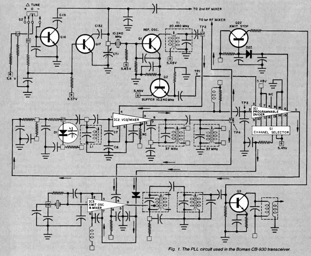
Fig. 1. The PLL circuit used in the Boman CB-930 transceiver.
Repeat the experiment while monitoring the potential at pin 6 of IC1. When the reference signal disappears, the potential on pin 6 drops to about 0.3 volt, reverse biasing Q22 and killing transmitter output. Interrupting the signal at pin 2 of IC2 causes the monitored potential to drop to practically 0, again triggering the transmit-stop circuit.
Substitute the output of a variable-frequency signal generator in the PLL system when you suspect vco failure as follows. Disconnect pin 2 of IC2 to simulate a missing vco signal at mixer-input pin 2. The vco frequency on channel 1 is 37.660 MHz- 20.480 MHz = 17.180 MHz. Using a frequency counter, tune the generator to 17.180 MHz and set it for about a 100-mV output. Feed a signal from a CB generator to the input of the receiver so that you know when the PLL begins operating.
When the 17.180-MHz output of the signal generator is fed to pin 2 of IC2, the signal from the CB generator should come through loud and clear, indicating that the PLL is working. When the transmitter is keyed, there may be no output at first. Then there may be a brief output that comes and goes as if the PLL is attempting unsuccessfully to lock. Confirm this by monitoring the lock voltage at pin 6 of IC1, where there should be regular fluctuation. Whenever the voltage at pin 6 rises to a level sufficient to reverse bias D22, there will be an output from the transmitter. This output will not remain since the PLL cannot lock because it does not have the control over the signal generator it has over the vco.
Due to instrument loading effects, very few frequency-counter readings are possible around the PLL. When the test probe is touched to pins 1, 2, 4, and 6 of IC2, PLL operation will cease. The 3.300-MHz mixer output at pin 9 is the only frequency you will be able to measure on IC2 (on channel 1). However, you can measure 10.240 MHz at the emitters of Q1 and Q2 and at pin 3 of IC1. You can also measure 3.300 MHz on pin 2 of IC1. On IC3, you can measure the signal frequency at pin 9 with the transmitter keyed, but the transmitter's output will cease every time the probe tip is touched to pin 9. If you use a frequency counter with a top end of 50 megahertz or greater, you can even measure 37.660 megahertz at TP4 (point 73 in Fig. 1).
If any frequency obtained by mixing two other frequencies can be measured, the two mix frequencies must be present. For example, if you cannot measure the IC2 vco signal nor the 20.480-MHz signal but are able to measure 3.300 MHz on pin 9, you automatically know the other two signals must be present.
Troubleshooting Examples. Many conditions can render a PLL system inoperative. Suppose, for example, that the reference oscillator stops working.
Without a reference, the PLL would not operate and the voltage on pin 5 of IC1 would be high and would not vary when switching through the channels. This is a clue that one of the inputs to the phase comparator is missing. Also the voltage on pin 6 of ICI would be near 0, another clue that one of the comparator's inputs is missing.
First, check for a 10.240-MHz signal at pin 3 of IC1. Finding nothing here, go directly to the oscillator. Check for the presence of r-f at the emitter of Q1; no r-f here pinpoints the trouble.
A missing vco signal will also cause one of the comparator's inputs to be absent. If the 1024 divider or the programmable divider is not working properly, it can cause one comparator input to be missing. A malfunctioning mixer in IC2 can also cause a comparator input to be missing.
Now, suppose the PLL is dead. About 5.5 volts is on pin 5 of IC1 and there is no output at pin 9 of IC2, but the reference oscillator is working. You must determine if the voltage at pin 5 of ICI is high because the vco stopped working or the vco stopped working because the voltage is so high as a result of some defect in IC1.
To determine where the fault lies, tune to channel 1 and feed a 3.300-MHz signal to the input of ICI via pin 2.
Assuming ICI is working properly, there should be near 0 volt on pin 6 until the correct frequency is applied to pin 2, at which time, the voltage should rise and fall as the PLL tries to lock. Monitor the voltage at pin 5 as you vary the frequency above and below 3.300 MHz.
There should be a voltage below but none above 3.300 MHz. These results are a good indication that IC1 is okay.
Suspicion is now on the vco or mixer in IC2. Generator substitution for the vco output is called for. Remove all connections from pin 2 of IC2 by cutting through the foil trace on the pc board.
Feed a 17.180-MHz (on channel 1) signal through a coupling capacitor to pin 2. Have a modulated signal feeding the input of the receiver so you know when and if the PLL starts to work. If it does, the problem is in the vco.
To determine if the trouble is within IC2 or in the external circuitry, measure the voltages on the IC pins. If this fails to produce results, you may have to substitute another IC and/or check all external components.
Summing Up. The material presented here is the result of actual tests and measurements on a commonly used PLL system. Using the material presented here as a guide, you should be able to troubleshoot virtually any CB PLL system you encounter. Note, however, that FCC regulations require any one repairing or adjusting the frequency-determining sections of a CB transceiver to have a First-Class Commercial license. However, a radio amateur who is modifying a CB PLL rig for 10-meter operation need not have the license.
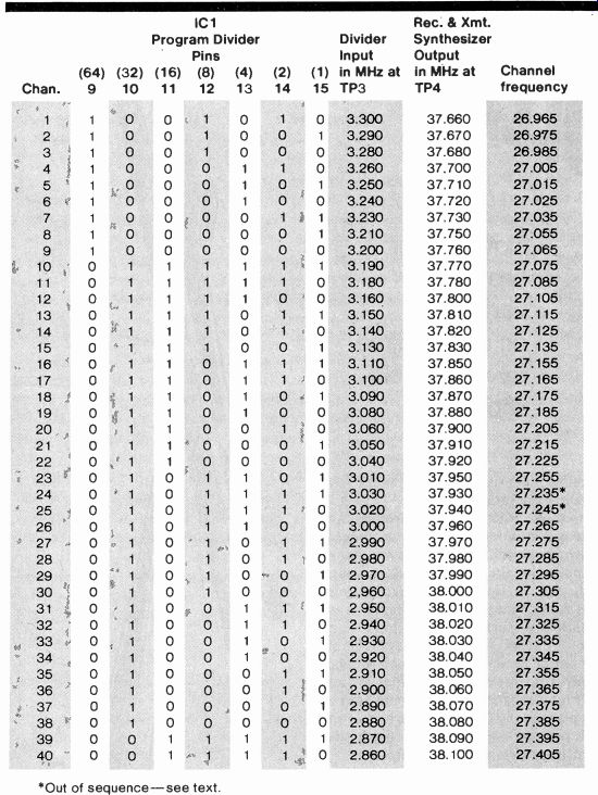
TABLE I--TRUTH TABLE FOR IC1 PROGRAMMING PINS