Here is a solderless breadboard development system that features six peripheral circuits!
By WARREN BACKER
THE UNIVERSAL DESIGNER DESCRIBED HERE SHOULD appeal to neophyte and professional alike. The key is the need for a solderless-breadboard development system. This one features six of the most-often-needed peripheral circuits used in conjunction with such systems. The best part of all is that the unit is always ready to serve the user.
You may have threatened more than once to build a few important circuits (like a set of LED's) and have them ready for any application as it may arise. Like most other experimenters, you never seem to get around to the task. Then, the next time you're working on a special project, you have to take the time to breadboard a set of readouts (or whatever) on the panel. That not only wastes time, but valuable breadboard space is also taken up by the needed circuitry. It is in cases like these that the Universal Designer comes to the rescue.
Aside from a good, regulated power supply, most experienced breadboard users will probably agree that a pre-wired set of Light Emitting Diodes (LED's) can save a lot of time if they can be connected quickly to the circuit under test. Other circuits that may be quite useful could include a set of seven-segment readouts, a clock generator, and a bounceless switch. In addition, there may be many specialized functions required by the experimenter's own field of interest.
The Universal Designer provides the answer for at least six of the more popular requirements of solder-less-breadboard systems. The importance of the LED's mentioned earlier has been covered by the eight LED's waiting to be used. The circuitry also includes a set of drivers to assist in reducing circuit loading. The input terminals of those drivers are connected to eight circuit pins that connect directly into the solderless breadboard you are using. One nice feature is an on-board switch allowing the experimenter to turn the indicators on and off as needed. That can be important if you are using a battery to supply power for your project design.
As mentioned, there is also the need for a bounce-less switch (pulser) in many design applications.
Again, that circuit feature has been considered in the Universal Designer. It provides , two such switches.
Even better, the outputs of those switches are connected to four circuitboard pins and will plug directly into your breadboard. In addition, by using selected pins you can generate a positive or a negative-going pulse when the switches are operated.
Another important circuit that is often needed is some form of a counter to keep track of one of our processes. The Universal Designer contains a dual-decade counter that can be used for up to 100 events (0 through 99). That circuit can be very helpful and would take considerable time and breadboard space if you had to wire it into your existing circuit board.
Sometimes it's handy to be able to read the quantity in normal decimal figures instead of counting in a Binary Coded Decimal (BCD) fashion. That is handled by the Digital Designer, by adding two seven-segment LED readouts. Of course, to use that feature, some sort of driver/decoder system must be included ahead of the indicators. Two decoder/drivers are on board for that requirement. They are hard-wired to the readouts and input signals (in a BCD format) are inserted through two sets of solderless connectors much like those used on the actual breadboard. The wires from those input pins can be connected directly to the output of the circuit under test. Just think of the space that would be required to wire that kind of circuit to your breadboard.
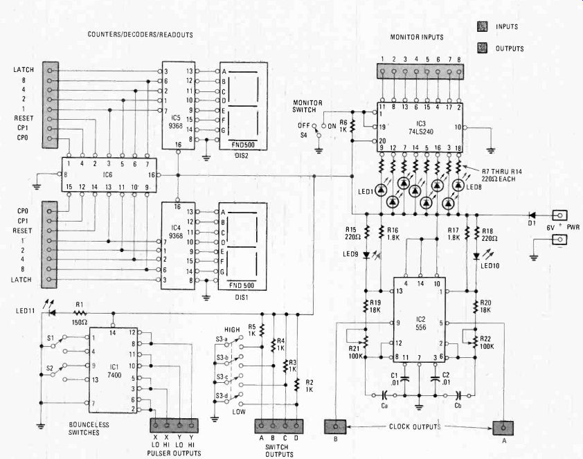
FIG. 1. COMPLETE SCHEMATIC DIAGRAM FOR THE UNIVERSAL DESIGNER project that
you can wire and use in one day. Should the schematic diagram appear to
be too difficult to understand all at once, look at Figs. 2 through 8 and
the text that describe these partial circuits. All doubts will clear up
quickly.
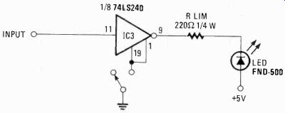
FIG. 2. LOGIC MONITOR LED CIRCUIT-one of eight. The driver in IC3 uses
power direct from the power supply and not the input signal. Thus, the LED
does not load down the input circuit when it comes on. When the input to
pin 11 is high, the output at pin 9 is effectively at ground potential thus
completing the circuit between the LED and the power supply-the LED will
glow.
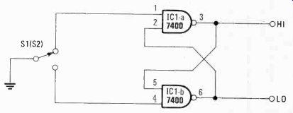
FIG. 3. BOUNCELESS SWITCH-one of two. The 7400 chip has four NAND gates
with two being used in each circuit. As shown, the switch position produces
a high (1) signal at pin 3. When the switch is thrown down, the outputs
reverse their states with a low (0) now appearing at pin 3.
Whenever you begin to design or experiment with electronic circuitry, you soon find you need to provide some kind of signal. While some experimenters already may have a good source of the most usable frequencies on their work benches, most will have to improvise some method of generating an input signal of the proper frequency. Here again the Universal Designer provides for the need as it includes two such clock generators. Each of them can be adjusted individually over a very wide frequency range. The timing capacitors and the setting of the frequency trimmer potentiometers provided gives you all the timing you are likely to need. The frequency trimmers have about a 10:1 control over each of the two frequencies. Upper frequency limits are constrained by the normal Limitations associated with the 556 dual-timer integrated circuit used.
Finally, one circuit supplied by the Universal Designer is an on-board set of switches that are used to program logic levels required for various counters and gates, as well as many other circuits. The choice of either a logic "0" or "1" may be made by pressing a switch lever. A handy feature, indeed.
Other features include power-input pins that allow you to connect the Universal Designer directly to the main breadboard being used. Those pins are placed in a position where they will mate with the normal positive and negative supply connections along the edge of most breadboard systems. In addition, if there is no such supply on the breadboard, the unit may be powered by a 6-volt battery. In that event, the voltage is dropped through a diode on the Universal Designer and it can then supply power to the main breadboard pins.
For those readers who must scan the complete circuit diagram of a project in advance of the theory of operation discussion, look at Fig. 1 now. However, partial diagrams illustrated in Figs. 2 through 8 coupled with the theory discussion makes life simpler for most readers. It is suggested that once the reader fully understands the operation of the circuit segments in each of the partial diagrams in Figs. 2 through 8, he should refer back to Fig. 1. Thus, the full versatility of the Universal Designer will become apparent in small doses.
Start to build your own
Construction of the Universal Designer is quite straightforward. Since no critical circuitry is involved, almost any kind of construction method can be used.
However, a compact unit is built by using a small printed-circuit board. The Parts List at the end of this article includes the source for such a printed-circuit board, as well as a complete kit of parts.
The easiest way to put the Universal Designer together is by using a printed-circuit board. Either make one from the foil template shown in Fig. 9 from .0625-in. single side board with 1-ounce copper, or buy it made, cut, drilled and silk-screened with call outs added. The complete schematic diagram for the Universal Designer is shown in Fig. 1 for those who wish to modify the circuit to their special needs. The board electrically connects to the solderless breadboard via a series of stake pins soldered to the board. Be sure these pins line up with the solderless board's mating holes.
You may want to mount the board and solderless breadboard on a sloping surface, build a power supply, or add other improvements. It's all up to you.
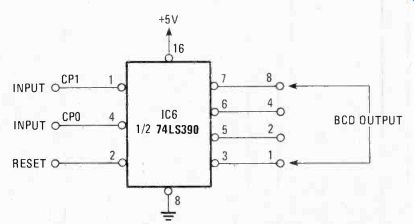
FIG. 4. DECADE COUNTER-one of two. With two independent counters, the board
offers the builder-designer the opportunity to either count to ten (0-9)
on two counters or count to 100 (0-99). IC6 is a dual unit (only one section
shown) with each section independent.
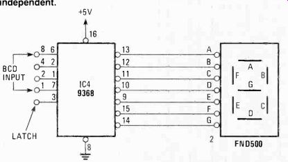
FIG. 5. BCD-TO-LED DISPLAY-one of two. The input to this circuit can either
be from the designer's circuit or direct from the decade counter shown In
Fig. 3. The driver, IC4, is hard wired to the LED display but IC4 can be
removed from its socket and other drivers can be used from any circuit to
drive the LED.
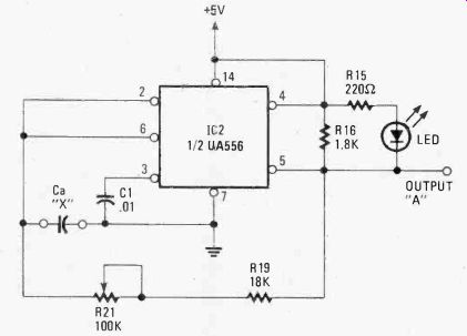
FIG. 6. CLOCK GENERATOR-one of two. You would expect to find two clocks
since 1C2 uses a 556 chip which is essentially two independent 555 timer
circuits in one chip package. Capacitor C2 can be substituted to obtain
different clock speeds. Both clock circuits are identical, but they may
be timed differently.
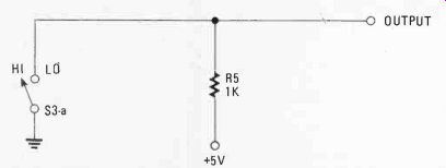
FIG. 7. LOGIC OUTPUTS-one of four. Then Universal Designer offers four
logic output controllers from four SPST switches packaged in a mini-dip
case. Four logic inputs usually are enough for most experimenter's projects.

FIG. 8. POWER DISTRIBUTION circuit is protected by a silicon diode. Under
normal hookup, the diode will drop about .7 volts from the external power
supply. If a permanent regulated supply is attached to the board, then eliminate
the diode and insert a jumper.
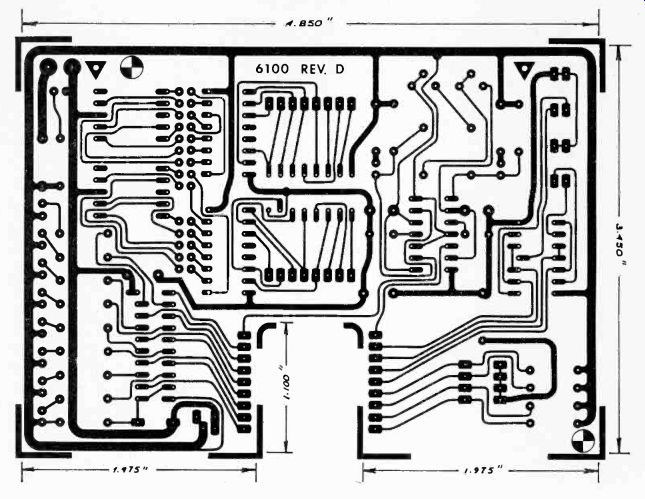
FIG. 9. TEMPLATE FOR THE foil side of the printed circuit board shown same
size.
To keep project neat and handy as the author intended it to be, be sure to use a circuit board for your project.
Circuit description
Each of the six functions provided by the Universal Designer are generated by standard circuits. Let's take those functions in the same order as they were presented earlier in the article. The eight logic-monitor LED's can be broken down into one LED and its drive circuit (see Fig. 2). In reality, the driver is one section of a 74LS240 IC that houses eight identical drivers.
That IC operates likes eight switches. When an input pin is provided a logic "0", it will produce a logic "1" at the output. Since a logic "1" is positive here, and the LED's are supplied with a positive source, the associated LED remains dark (unlit). However, when the input is presented with a logic "1" (high) the IC's output shifts to a logic "0" (low), the LED lights.
In addition to the eight inverters included in the 74LS240, that IC also provides two inhibit pins to allow the outputs to be turned off when desired. The way we use it, both pins (No. 1 and No. 19) are tied together and grounded if we want to use the LED's. If we do not want to use them, simply leave the inhibit pins undergrounded. One main advantage of using the driver IC is that all the current for the LED's must be carried by the 74LS240 and not by the circuit under test.
The next circuit to be covered is the bounceless switch (see Fig. 3). Such circuits are also referred to as "pulsers" since they can provide a controlled output pulse of either logic "0" or logic "1" with no contact bounce. Such pulses are used to trigger certain circuits or to advance counters at a controlled rate, as well as checking the operation of gates, etc. Study Fig. 3. You can see that the switch consists of two NAND gates; each contains two inputs. With the conditions shown, gate "A" has one of its inputs held at logic "0" assuring that its output is logic "1." At the same time, gate "B" has both its inputs at logic "1." That forces the output pin to be inverted to the indicated logic "0." When the input switch is pressed, conditions are reversed and the outputs change state momentarily.
The output pulses are clean and free of any of the glitches commonly associated with normal spring-type switches. The SPDT switch at the input terminals of the gates is a momentary pushbutton switch. Since the 7400 IC contains four 2-input NAND gates, the package can support two such switch units. That is the heart of the Universal Designer's bounceless switches-a simple device, but one that is often very important to design work.
Figure 4 shows a basic decade counter which is one-half of a 74LS390 IC. As the circuit shows, the counter has two inputs and one reset pin for control applications.
All are terminated at the eight-pin connector located next to the IC. The output from the counter is in a BCD format and is also terminated at four other pins of the previously mentioned 8-pin connector. This circuitry makes an easily used decade counter available to the experimenter; to make it requires little bore than the insertion of a few wires into the holes of a connector. Since the 74LS390 is a dual-decade counter, there are really two such counters available on the Universal Designer board. Each of the counters can be used separately, or they can be used as a pair as needed. When cascaded, they can count to 100 (0 through 99). Directly connected to the decade-counter output circuitry are two BCD to seven-segment decoder/driver integrated circuits. A review of Fig. 5 reveals that the circuitry is very common (and easily constructed). The 9368 is a BCD to seven-segment decoder and driver. It is hard-wired to a standard seven-segment readout. I used an FND500, but other devices can be substituted.
In operation, BCD information is applied to the decoder's input at the eight-pin connection block.
To be exact, the decade counter is always connected to the decoder inputs. That makes the board easier to construct. (Note: remove IC6 for direct inputs to IC4 and IC's.) In fact, since BCD information is required for proper decoder operation, it becomes a natural to use with the decade counter(s). As with the other circuitry, that feature is duplicated. Therefore, two 9368's and two FND500's are required to display BCD information up to a reading of 99 (0-99= 100) on the seven-segment readouts. When you consider the usefulness of the last two features, it is not difficult to imagine the huge amount of breadboard space (and time) you can save by using the Universal Designer with your next project.
A clock generator
Any piece of equipment intended to assist the designer, builder, or experimenter would have to include some sort of a "clock" generator if it were to be a really worthwhile accessory. The Universal Designer does not let you down. Would you believe that it has not one, but two, complete oscillator circuits on the board with all the other features? Fig. 6 is the circuit of one of them. The heart of the "clock" system is a standard eA556 timer IC. (The 556 is actually two 555's in one package.) As Fig. 6 shows, it is straightforward and non-critical to construct. The 100K potentiometer connected to pins 2 and 6 is the fine-frequency adjustment for the oscillator. Capacitor "Ca" connected from the same pins to common ground (pin 7) is the main timing capacitor. The board has two Molex-type connectors to permit easy insertion of various values of capacitance in the circuit.
Each one of the two clocks can operate independently.
For example, oscillator "A" could be used as a reference "clock" for the counter while oscillator "B's" frequency could be counted. Another feature of that oscillator section is the addition of an LED indicator at the output of each oscillator. (Note the LED from pin 4 to pin 5.) That device lets you monitor the oscillator's activity and is especially handy when using low-frequency pulses.
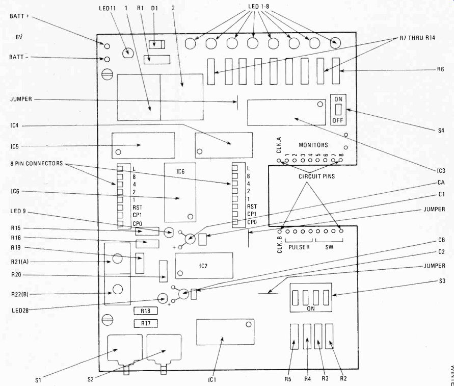
FIG. 10. HERE'S THE UNIVERSAL DESIGNER OUT LINE with all the circuit parts
installed on the circuit board. To see how the Universal Designer mounts
on a solderless breadboard, refer to the photograph on the first page of
this article.
Logic switches were the last items to be mentioned at the beginning of this article and their circuitry is in Fig. 7. Once more, there is nothing exotic or elaborate about the feature. Yet, that circuit is very useful in breadboard applications. As shown, the switch simply pulls a level to logic "0" by grounding the point, or to logic "1" by making it possible to apply a DC voltage, through a IK resistor, to the unit under test. Simple and effective, it will save both time and breadboard space. Four of those simple circuits are provided by the Universal Designer and are contained on an eight-pin mini-DIP switch unit.
-----------
PARTS LIST
RESISTORS
All resistors 1/4-watt unless noted R1-150 ohms R2-R6-1000 ohms R7-R15, R18-220 ohms (see text)
R16, R17-1800 ohms R19, R20-18,000 ohms
R21. R22-100,000 ohms, trimmer potentiometers
CAPA C1TORS
C1, C2-.01 ceramic disc Ca. Cb-0.1 ceramic disc 2.2-4F electrolytic 22-4F electrolytic SO L1D-STATE DEVICES D1-1A silicon diode DIS 1, DIS 2-FND-500 seven-segment displays I C 1-7400 IC2-556 IC3-74LS240 IC4, IC5-9368 or 4368 (see text)
IC6-74LS390 LED1 thru LED11-red light emitting diodes MISCELLANEOUS S1, S2-pusbutton switches, momentary contact, normally open S3-4 position DIP switch S4-1 position DIP switch 8-pin sockets (2)
16-pin IC sockets (1)
Small PC pins (20) PC sockets (4)
Alligator clips/insulators (2)
4-40 x We Nylon spacers (2)
4-40 x 1/4 Nylon spacers (2)
PC board (optional)
Case, hardware, etc.
The following items are available from Etronix, 14803 NE 40th, Redmond, WA 98052.
6100 Kit $49.95
6100
Assembled $59.95 QT59B
Breadboard (2 required) $ 2.99 ea.
QT59S Breadboard $12.50 ea.
PCB1 LEDI-LED11 DISP-1,2 U-3 U-4,5 U-6 R-21,22 S-1, S-2 S-3 S4
Misc
PARTS
$20.00 ea.
.12 ea.
.95 ea.
2.25 ea.
2.50 ea.
2.65 ea.
3386P-1-104100K Trimmer Pots .40 Pushbutton 1.20 JS-8750-04 4 Pos Dip Sw 1.60 JS-8750-01 1 Pos Dip Sw 1.25 Molx 0204-1112 Socket Pins .10 Moix 2202-2081 Strip Socket (2 req'd)
T46-4-9 Stake Pins (22 required)
6100 Printed Circuit Board L-72RD (10 Red LED's)
FND500/503 (2 required)
74LS240 9368PC (2 required)
74LS390 ea.
ea.
ea.
ea.
ea.
.40 ea.
.04 ea.
Please note that supplier's parts symbol designations vary slightly with those given in this article. For example: IC1 is supplier's U-1.
-------
Using the Universal Designer
In use, the Designer is normally plugged into one of the boards of your solderless-breadboard system.
The power pins mate with the two rows of connectors along the edges of most breadboard systems. Use them to supply power to the breadboard if you use the battery-supply connections on the Universal Designer, or to transmit power to the Universal Designer if you take the power from the main system. If your system has other than standard power rows (such as the "Experimenter" series) then you will have to modify your board accordingly.
----------
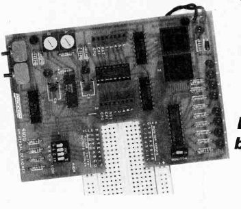
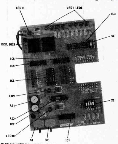
-- THE UNIVERSAL DESIGNER looks like this after the last part is soldered into place. This photo duplicates Fig. 10 on the-previous page. Now fit the printed-circuit board onto a solderless breadboard and you are now set up to experiment with your next dream circuit.
When connected as outlined, most of the major connections are then made between the breadboard and the Universal Designer through two rows of nine pins each. Of course, that means that the user will have four holes available in the breadboard for each of the eighteen pins to which he (or she) may connect wires to the circuit(s) being tested. Earlier, we mentioned that certain signals would be inserted through two eight-pin connectors on the board being discussed.
That is still true and they will be used for input and output information relating to the decade counters and the seven-segment decoder/driver circuitry.
We said that batteries could be used to power the unit. Since TTL logic is based upon a 5-volt supply, further mention of that circuit is in order. A convenient battery to use with the Universal Designer is a 6-volt lantern-type battery. Connections to the board for such a supply are automatically applied through a silicon diode that will drop the voltage to approximately 5.4 volts (see Fig. 8). That is within the specs of TTL IC's. Of course, other digital devices may use different voltages. In fact, one of the more popular systems today is CMOS. It can be operated over a wide range of voltages. However, of all the various units, TTL is probably the least forgiving of supply-voltage variations.
Building tips If you are the kind of builder that likes to go his own way, then use the printed circuit foil template shown in Fig. 9 to make your own board. You may wish to omit some circuit sections; or, you may wish to increase the duplication of some circuit sections for the common applications peculiar to your needs. Just do your thing, but use a circuit board because point-to-point hard wiring is difficult in this instance. Should you elect to purchase the kit of parts or 6100 printed circuit board itemized in the Parts List, your finalized project with all the parts in their proper place like in Fig. 10.