Source: Radio Electronics--Electronic Experimenter's Handbook (1993)
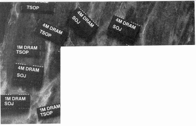
An overview of today's revolutionary memory technology-and a peek at tomorrow's.
by STEPHEN J. BIGELOW
STORAGE AND RETRIEVAL OF DIGITAL information has sparked an exciting revolution in computers and consumer electronics. You find semiconductor memories in nearly all "intelligent" electronic systems, including car radios, televisions, VCR's, compact-disc players, and computers. Without the on-going advances in memory technology, the high-tech revolution would rapidly grind to a halt.
In this article, we will examine several important concepts be hind semiconductor memory devices, including basic technologies, memory organization and configuration, design considerations, and applications.
Memory types
Semiconductor memory devices can be classified in one of two ways: permanent or temporary. Although basic operating principles of both are similar, each plays a different role, and each has unique advantages and disadvantages. We will discuss both types in detail.
As the name suggests, information in permanent memory is retained at all times, even after removal of system power. Permanent memory is also called non volatile and read-only memory.
Permanent memory is most often used to store fixed program instructions or numerical constants that do not change during the life of a product. For example, personal computers use permanent memory to hold the basic input/output system (BIOS) that initializes the computer and provides it with a core of low-level functions. There are four basic types of permanent memory: ROM, PROM, EPROM, and EEPROM. Let's discuss each type.
ROM
The read only memory (ROM) is the oldest and most straightforward type of permanent semiconductor memory. The information that's programmed into a ROM is specified by the buyer, but the ROM itself must be built by the manufacturer.
A ROM is relatively inflexible after it's been programmed, it can never be altered. If the information in a ROM must change, a whole new device must be manufactured and substituted for the old ROM, and that is an expensive, time-consuming process. Hence the ROM is economically feasible only when used in great volumes for thoroughly debugged applications.
One advantage of the ROM is its ruggedness. Since the pro gram is an actual physical part of the device itself, it can withstand relatively large amounts of electrical and physical abuse, yet still maintain its contents. The auto mobile industry uses ROM's extensively in on-board computers.
PROM
The programmable read only memory (PROM) offers a tremendous advantage over the ROM in that it can be programmed by the end user, who is then less dependent on manufacturers' lead times. A PROM can be "burned," or programmed, only once be cause it cannot be erased.
The term burn comes from the method used to program a PROM. A factory-fresh PROM consists of a matrix of fusible links. An intact link produces a binary 0 at the selected location; a burned (open-circuit) link produces a binary 1, as shown in Fig. 1. (We'll discuss how to get at a particular location in a PROM later in this article.) To burn a PROM, a special piece of equipment called a PROM burner generates high-energy pulses which destroy the desired links to match the contents of a user data file.
PROM's are slightly more expensive than ROM's on a per-unit basis, but their flexibility often justifies higher cost. Many PROM's are available through re tail electronics outlets.
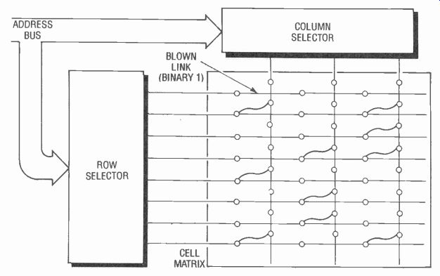
FIG. 1--A PROM BEFORE PROGRAMMING consists of a matrix of fused links
joining each row-column intersection. Programming blows desired links.
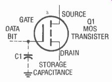
FIG. 2--IN AN EPROM, CAPACITANCE across the gate-drain junction of a MOS
transistor provides storage.
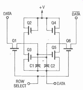
FIG. 3--A FLIP-FLOP is the basic unit of storage in static RAM devices.
EPROM
The erasable programmable read-only memory (EPROM) over comes one of the main disadvantages of the PROM: its inability to be reused. After a link has been burned, it can never be restored.
By contrast, typical EPROM's can be reliably burned and erased thousands of times.
The PROM is built around traditional bipolar transistor technology, which uses both a great deal of power and occupies a lot of space. The EPROM, on the other hand, uses newer metal-oxide semiconductor (MOS) technology, which requires little current and occupies little space. In an EPROM, information is stored as small packets of charge buried deep within the substrate of the IC, as shown in Fig. 2.
An EPROM is programmed much like a PROM. A special EPROM programmer selects an address in the device, places the desired binary information on the data lines, and then pulses the EPROM's PROGRAM pin. That pulse is what locks the bit pat tern into the substrate of the chip.
To erase an EPROM, it's necessary to remove the charges in the IC's substrate. That's accomplished by exposing the circuit (the die itself) to short-wave length ultraviolet (UV) light for a prescribed period of time. The excitation created by the UV light allows stored charge to dissipate, so the IC gradually returns to its pre-programmed state. The UV light is introduced into the EPROM through a transparent quartz window in the top of the IC package.
Use caution when working with EPROM's. Even though it takes about 20 minutes of exposure to a concentrated UV light source to erase an EPROM, some common sources of light, such as sunlight, fluorescent light and "black-light", may contain enough UV to trigger random charge dissipation and introduce errors in the device. So be sure to cover the quartz window with a piece of opaque material.
EPROM's cost more than PROM's, but cost-per-bit is actually lower because MOS technology allows the designer to squeeze several times more information in the same amount of space. One disadvantage of the EPROM is that it must be physically removed from the system to be erased and re-programmed.
EEPROM's The electrically erasable programmable read only memory (EEPROM) is similar to the EPROM, but overcomes its main disadvantage: the inability to program it in-circuit. That feature offers exciting possibilities in applications where software must adapt to changes in the operating environment.
The EEPROM is no panacea, however. It's slower than other types of memory, and it requires a relatively long time to update the altered data. As a result, EEPROM's are best suited for holding information that changes infrequently. Information that changes often is best left to the work of temporary memory; the other broad class of semiconductor memory.
Temporary memory
Information held in a temporary semiconductor memory device can be altered and updated frequently, but will be maintained only as long as power is supplied to the device. If power fails, memory contents will be lost. That type of memory is usually referred to as volatile memo ry. It is also known as random access memory (RAM). The name refers to the fact that any location may be accessed as quickly as any other. By contrast, in a sequential device like a tape drive, access speed depends on the lo cation of the desired information. However, random locations in ROM's, PROM's, EPROM's, and EEPROM's can be accessed with equal speed. Nonetheless, when people speak of RAM, they almost invariably are referring to temporary memory.
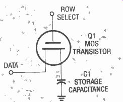
FIG. 4-CAPACITANCE is the basic unit of storage in the DRAM.
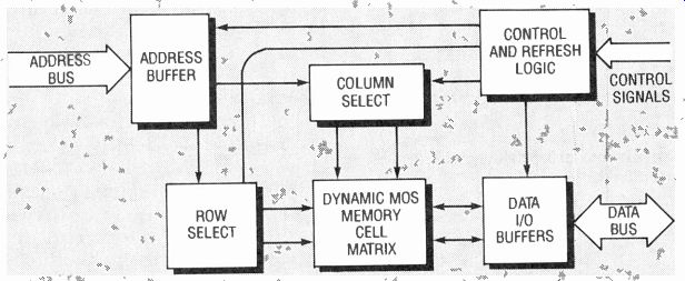
FIG. 5-INTERNAL DRAM STRUCTURE. The control refresh circuitry increases
complexity but drastically increases storage capacity.
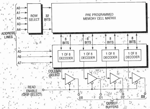
FIG. 6-A BASIC ROM consists of row- and column-select circuitry, the memory
array, and three-state output buffers.
Most electronic processing systems require at least some RAM.
The amount that's required depends on the application. A simple system, such as a programmable digital thermostat, may require only a few bytes of RAM. But a computer may require mil lions of bytes of RAM.
There are two basic types of RAM: static and dynamic. Each type has particular benefits and drawbacks.
Static RAM
Static RAM (SRAM) is the oldest and most straightforward form of temporary semiconductor memory. A typical SRAM consists of several flip-flops, or cells, as shown in Fig. 3. Each cell stores one bit of information; multiple cells are arranged in a two-dimensional array. 'lb access a particular cell, row and column addresses must be set up, and then several control signals must be pulsed.
Since data is always available from the flip-flop matrix, the SRAM tends to be a fast device.
Its primary disadvantage is limited capacity. Each flip-flop occupies a relatively large area on the IC, so the maximum number of cells is limited.
Dynamic RAM
Dynamic RAM (DRAM) uses an entirely different technology to accomplish data storage. The key difference lies in the design of the cell itself. As shown in Fig. 4, each cell in a DRAM stores information as a packet of charge across a MOS transistor, similar in principle to way the EPROM works, but it is unlike the SRAM, which uses a flip-flop to hold one bit of data.
To allow frequent updates, each cell must be capable of changing state almost instantly.
To allow rapid change, the storage capacitance must be extremely low, so low in fact that it cannot sustain its charge for more than a few milliseconds.
Therefore each DRAM location must be refreshed about every two milliseconds. If a cell is not refreshed, it will simply lose its data. However, refresh cannot happen by itself; external circuitry is required, as well as additional circuitry within the DRAM itself. Fig. 5 shows a block diagram of the internal structure of a DRAM. The added complexity and cost of refresh circuitry is the main disadvantage of DRAM.
On the other hand, DRAM offers several distinct advantages over SRAM. Storage capacity is much greater. Common DRAM's provide one megabit (22°) of storage, and four-megabit IC's are just over the horizon. In addition, 16-megabit memories are being developed, and 64-megabit DRAM's are on the drawing board.
Power is another consideration. DRAM's require less current to operate; there are far fewer components per cell to dissipate power. The power savings can be substantial in applications that need a great deal of memory.
DRAM's also have a standby mode that essentially disables all functions except refresh. In standby mode, a DRAM requires just a few milliwatts of power to maintain its information. In some cases, the low power requirement makes battery backup practical. SRAM's also have a standby mode, but they typically need more than 100 milliwatts of power. Now let's examine some of the technologies used to fabricate semiconductor memory devices.
Fabrication technologies
Every semiconductor memory chip houses sophisticated, sensitive microcircuitry. Each minute component must be integrated deep into the substrate of the chip (or die), which itself rests within a hermetically sealed case of plastic or ceramic. The process of circuit integration involves a complex combination of optical and chemical processes to form a working IC. Memory devices manufactured today are typically made using either bi polar or MOS fabrication technologies. In addition, a new hybrid of the two technologies, called Bi-MOS, has begun to appear. Although the actual manufacturing processes of these kinds of devices are too involved to cover here, we can review the characteristics and uses of those technologies.
Bipolar technology
The bipolar transistor (with emitter, base, and collector) was the first component successfully integrated into a semiconductor wafer in the form of the TTL IC.
Many simple logic functions could thus be synthesized easily and efficiently. The resulting low cost and high availability made TTL a mainstay of digital logic design through the 60's and early 70's. Even to this day, TTL re mains a cornerstone of basic logic design. When memories were needed, TTL was the obvious choice.
Although there are several SRAM chips in the TTL family (notably the 74S200 and 74S201), TTL suffers from several major drawbacks that severely restrict the capacity of bipolar SRAM. First, bipolar logic requires a relatively large area on the chip for each logic gate. Many gates are needed to build a SRAM, so space is depleted rapidly. In addition, bipolar logic requires significant operating current per gate. Since current ultimately translates into heat, the number of cells is limited even further. Size and power restraints usually limit the number of bipolar memory cells to fewer than 1000 bits.
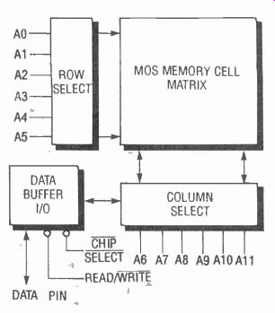
FIG. 7--THE BASIC SRAM is more complicated than a ROM because of the addition
of a READ WRITE line.
MOS technology
The development of MOS technology is largely responsible for the incredible advances in high tech electronics since the late 1970's. The materials and chemicals used in MOS fabrication are different from those used for bi polar fabrication, but the process is fundamentally the same. The most familiar MOS family is complementary MOS (CMOS), but there are many variations, including PMOS, NMOS, VMOS, DMOS, and HMOS.
CMOS, NMOS, and HMOS devices are the most widespread variations of MOS technology in use today. CMOS has been used extensively in memories, and to produce a family of devices that is functionally similar to the TTL family. CMOS dissipates far less power than TTL and can run on a much wider range of supply voltage (3-15 volts DC). N-channel MOS (NMOS) technology is used to produce memories that are fast, dissipate little power, and can fit many components on a chip. Although early devices required several supply voltages, modern NMOS IC's operate from a single 5-volt supply. High-performance MOS (HMOS ) is an NMOS variation that's used in modern high-speed low-power microprocessors.
In spite of their obvious advantages, all MOS devices suffer from one key weakness: they're extremely sensitive to static electricity. There are important pre cautions that should be taken.
Be sure to follow manufacturers' guidelines for handling MOS devices.
Memory operations
To the external world, the organization of a semiconductor memory device appears as a sequence of locations. Each location may have 1, 4, 8, or some other number of bits, but regardless of the number of bits per location, each location has a unique address. The number of unique addresses depends on the number of address lines. If there are 8 address lines, then there are 28 or 256 addresses. Although externally a semiconductor device appears to have a sequential organization, internally the cells are arranged in a square.
The relationship between the number of physical cells (bits) and the number of logical locations (addresses) depends on the number of bits per address. For example, a memory IC could have 1 megabit of cells arranged as 1 x 1 megabit, as 4 x 256K, or even as 8 x 128K. Internal decoding circuitry varies depending on how the organization is to appear externally.
For example, Fig. 6 represents a simple ROM. The format of the ROM is 256 addresses with four bits per address. The memory array is a 32 x 32 square, giving 256 addresses. And for 256 ad dresses the chip requires eight address lines (2^8 = 256) to identify each location uniquely. The lower five address lines (A0-A4) select one of 32 possible rows (2^5=32). The upper three (A5-A7) select one of eight columns (2^3=8). There are four 1-of-8 decoders, so four columns (one from each group of eight) will be active for each selection.
After a valid address is presented to the address lines, the data bits at the intersections of the selected row and columns will be sent through the respective 1-of-8 decoders to several three-state buffers. If the READ ENABLE signal is brought low, the data present at the buffers will be de livered to the ROM's output. But when READ ENABLE is high, the high impedance of the three-state buffer will simply disconnect the ROM's outputs from the circuit.
SRAM's, along with PROM's, EPROM's, and EEPROM's, are more sophisticated. Figure 7 shows a simple SRAM organized as 4096 x 1. Addressing is similar to the ROM in the previous example but, in this case, there are 12 address lines that provide 212 or 4096 (4K) addresses. One bit of data is available at each ad dress location.
A READ/WRITE control signal determines whether data will be read from or written to the IC. If R/W is logic 1, data will be read from the cell. If R/W is logic 0, data will be written to the cell.
To read a bit of data, a valid address must be supplied, R/W must be high, and the CHIP select input must be low. To write a bit of data, the same conditions apply except that R/W must be low.
The timing relationships between the signals at various pins can be critical, depending on the circuit.
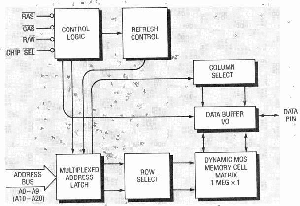
FIG. 8-DRAM KEEPS PIN COUNT LOW by multiplexing address lines on half the
expected number of pins. CAS and RAS signals strobe low- and high-order
address lines into the IC as necessary.
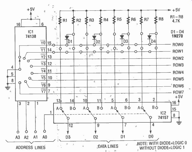
FIG. 9--BUILD AN EPROM EMULATOR from two TTL IC's, eight resistors, and
a number of germanium diodes. Place a diode across each row-column intersection
that is to be a logical 0.
Timing considerations Today's generation of RAM IC's has been designed to operate at high speeds, so timing characteristics for address, data, and control lines are important.
There are several important parameters that we will discuss.
Access time specifies how long it takes after addressing a specific location before valid data appears at the IC's output. A slow memory device may have an ac cess time of as much as 450 nanoseconds, while a fast device might access data in as little as 25 nanoseconds. Common memory devices today have access times of about 100-150 ns. As a rule of thumb, the faster a memory device is, the more expensive it will be.
Settle time specifies the amount of time that must pass after setting up the address, data, and CHIP SELECT signals, before the RAv may be pulsed low to write data into the IC.
In addition, the WRITE pulse must be held low for a minimum amount of time to ensure that the data is accepted into memory.
That is the duration of the write pulse. The address, data, and en able signals must be held steady for a minimum time after the write pulse; that period is called the hold time.
Those timing parameters apply to SRAM's; DRAM'S have even more intricate timing requirements. Although the basic principles of reading and writing are similar to those for the SRAM, there are some extra features and parameters that must also be considered.
The first involves memory ad dressing. As discussed earlier, DRAM's can provide millions of bits on one device. For example, addressing 1 megabit (22°) would require 20 address lines. It's possible to build an IC with 20 or more pins, but to save space and reduce pin count, several address lines are multiplexed on a single pin.
Figure 8 shows the block diagram of a 1-megabit x 1-bit DRAM. Note that only ten address lines enter the IC, so you might think that you could access only 21° (1024) locations. In fact the 20-bit address is broken up into two parts, each of which is sup plied separately. The lower ten bits select the desired row in the memory array, and the upper ten bits select the desired column.
The row-address lines are strobed into the IC by pulsing the row address strobe (RAs) input, and the column-address lines by pulsing the column address strobe (cAs) input. External circuitry must ensure that the proper set of address lines is applied to the IC before pulsing a strobe input.
After the IC receives the full ad dress, CHIP SELECT and R/W maybe set up, as with an SRAM, to read or write data. The access, setup, and hold times apply to DRAM's as well.
Refresh
As mentioned earlier, DRAM's require periodic refreshing, otherwise their stored charge will dissipate. There are several ways of refreshing a DRAM system, all of which use the RAs and CAS inputs. The simplest method is called RAS-only refresh. It involves holding CAS high, which in turn holds the output in a high-impedance, or disconnected, state. The refresh circuitry then selects each row in turn, pulsing RAs low for each row as it is ad dressed. It does not matter whether all rows are refreshed in one sustained burst, or one row between, for example, read or write operations. As long as a cell is refreshed in time, its data will remain intact.
Hidden refresh is a variation on RAS-only refresh in which CAS is held at logic 0 (for example, valid data is maintained on the output) while rows are selected and refreshed. Depending on system timing, CAS may be held low for several microseconds, during which several rows may be refreshed.
There are other variations, but all refresh circuits add a fair amount of complexity to a circuit. Fortunately, however, there are refresh-controller IC's for many different DRAM sizes and configurations. Those IC's reduce cost, increase reliability, and de crease required PC board space.
EPROM emulator You can easily assemble your own hand-made "EPROM" using two common TTL IC's and several Germanium diodes. Figure 9 shows the schematic for a 16 x 4 memory circuit. It's loosely called an EPROM because it can be re programmed at any time by rear ranging the diodes in the matrix.
Although the circuit is unsuitable for high-performance or microprocessor-based applications, it can be used to supply pre-programmed bit patterns to discrete logic circuits. It also provides an excellent demonstration of basic memory operation.
There are eight rows and eight columns, yielding 64 bits of memory. Two demultiplexers allow access to a particular memory cell. One demultiplexer de codes the row and one decodes the columns. A 74138 1-of-8 decoder selects the row, and a 74157 quad two-input multiplexer selects the columns. Address lines Al A3 drive the 74138 to select which one of eight rows will be pulled to ground. The columns are arranged in pairs; address line A0 determines which member of a pair is connected to the output.
The 1N270 diodes determine the bit pattern in the circuit. Germanium diodes are used because of their low forward voltage drop (0.3 volts); silicon diodes have a higher voltage drop and will not work with TTL IC's.
Every column is pulled high via a pull-up resistor. If a diode is absent when a particular row is selected, the column will provide a 5-volt output. However, if a diode is in place, it will be forward biased via the pull-up resistor, through the 74138, and then to ground. The corresponding output thus becomes a logical 0.
For example, if address 0000 is selected, 74138 output YO (row 0) is connected to ground, and all 74157 inputs are connected to the B position. Because there are diodes connected to each the B inputs in row 0, the output would be 0000. If the address was 0001, row 0 remains selected, but the 74157 inputs are switched to the A position. The A cells have no diodes, so all outputs would be high (1111).
Parallel memory
Semiconductor memories (both temporary and permanent) can be placed in parallel to increase the number of data bits available per address, as shown in Fig. 10. The circuit is built from several 2147 SRAM's (4096 x 1). By connecting the ad dress and control lines in parallel, the same address in all IC's will be selected simultaneously.
The data bits, of course, are kept separate. You could just as easily place 8, 16, or 32 IC's in parallel to create 4K x 8, 4K x 16, or 4K x 32 memory blocks.
Conclusion
Memory is an integral part of the high-tech revolution. Even the most basic processing circuit would be useless without some sort of memory to store variable data.
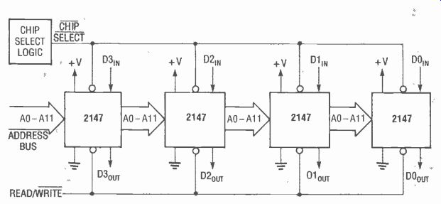
FIG. 10--BLOCK DIAGRAM OF A 4K x 4 static RAM array-parallel memory IC's
increase bus capacity.
As you can see from our comparison of the many different permanent memory devices, there are distinct advantages and limitations to each type. What you choose depends on your individual needs-the ROM is inflexible but rugged, while the PROM can be programmed by the user, but only once because it can't be eras ed. The EPROM can be programmed and erased over and over again but uses a lot of power and space, while the EEPROM can be programmed while in circuit, but is slow.
Useful Troubleshooting Hints & Tips