Introduction
THE preceding text has shown the usefulness and the versatility of transistors and has also mentioned their chief disadvantages, namely the temperature-dependence of their characteristics and the restricted upper limit to their working frequencies. Of these limitations the last-mentioned is probably the most serious and efforts are constantly being made to improve the high-frequency performance. There are a number of new techniques under development which seem to offer great promise and there is no doubt that the next few years will see increases in the working frequencies of transistors. In conclusion we shall list what appear ...
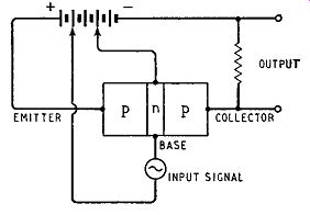
Fig. 14.1. Basic features of tetrode transistor
... to be the most important new types of transistor. In some of these, improvements in the high-frequency performance are obtained by reducing the base resistance rbb', the collector capacitance Cb' c or both.
Tetrode Transistor
The tetrode transistor is similar to a conventional pop or npn triode transistor but has two base connections arranged as shown in Fig. 14.1. One connection is treated as the input terminal as in a conventional transistor and the other is connected to a source of steady potential, negative with respect to the emitter potential in a pnp tetrode transistor. This steady base bias reduces the effective area of the base-emitter junction by forcing the current carriers towards the input connection, thus reducing the effective area of the emitter-base junction and hence the base resistance Tbb' and the collector capacitance cb'c. The transverse bias of the base region increases the length of path the injected carriers have to travel to reach the collector, increases their chances of neutralization and thus reduces the value of exand ex'. Surface-barrier Transistor
This type of transistor employs a thin slab of semi-conducting material to the opposite faces of which metal electrodes are attached to form the emitter and collector connections. Two circular recesses are etched in the semi-conducting material until the wall ...
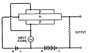
Fig. 14.2. Basic features of field-effect transistor
... is thin enough to give the required high-frequency performance.
Electrodes are then deposited in the recesses by electrolytic action, this being essential to obtain the necessary perfection of contact between the electrodes and semi-conducting material. By this means it is possible to produce transistors with cut-off frequencies of the order of 50 Mhz and with collector capacitances as small as 3 pF.
Field-effect Transistor
This is a form of transistor operating on principles entirely different from those of point-contact and junction transistors.
Provided the manufacturing difficulties can be overcome, this type of transistor offers great possibilities as a v.h.f. amplifier. It consists of a thin slab of high-resistance germanium (say n-type) through which a longitudinal current is passed as indicated in …
Fig. 14.2. On either face of the slab are two thin layers of low resistance
(p-type) germanium. The pn junction formed between the p-type and n-type
material is biased in the reverse direction to produce areas adjacent to
the junction where there are very few current carriers.
Thus the longitudinal current flowing in the centre slab is confined to a region near the centre of the slab where current ...
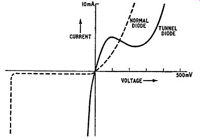
Fig. 14.3. Characteristic of a tunnel diode (solid) compared with that of
a normal junction diode ( dashed).
... carriers still exist. By increasing the reverse bias, the longitudinal current can be reduced and if a signal to be amplified is connected in series with the bias, the longitudinal current can be modulated and an amplified output can be obtained by passing this current through a suitable impedance. The input resistance of such a transistor is that of a reverse-biased diode and is therefore much higher than that of a conventional transistor the input resistance of which is that of a forward-biased diode.
Tecnetron
This is a semi-conducting device of French design which may be regarded as a development of the field-effect transistor. It consists of a crystal of, say, n-type germanium in the form of a cylindrical rod with a narrow neck near the centre surrounded by an indium ring. A current is sent along the rod via electrodes at the ends and a negative control voltage is applied between the ring and one end of the rod. This control voltage produces an electric field within the rod which deflects current carriers towards the centre of the rod. The conducting cross-section and hence the resistance of the rod thus depend on the applied signal. The device is claimed to have a mutual conductance of over 0.5 mA/V at 200 Mhz with an input resistance of the order of 1 M-ohm shunted by 0.2 pF.
Tunnel Diode
A pn junction with a very thin junction region has a characteristic shaped as shown in the solid line in Fig. 14.3: for comparison the characteristic for a diode with a thicker junction region is given in dotted lines. As would be expected breakdown for the thin junction diode occurs at a very low value of reverse bias and indeed there is in effect no region of high reverse resistance. An unexpected feature of the characteristic is, however, the region of negative slope which occurs at a forward bias: this was first reported by Esaki...
CONTROL ELECTRODE
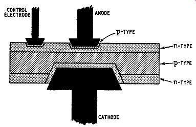
Fig. 14.4. Construction of a controlled rectifier
...in 1958. Such a pn junction can be manufactured with very low capacitance and oscillators making use of the negative-resistance kink can function at frequencies as high as thousands of Mhz.
These diodes are termed tunnel diodes and offer great promise as very high-frequency oscillators although the power output is very limited. They can also be used as high-frequency amplifiers but because the tunnel diode has only two terminals there is no isolation between the input and output circuits and it is very difficult to construct a cascaded amplifier.
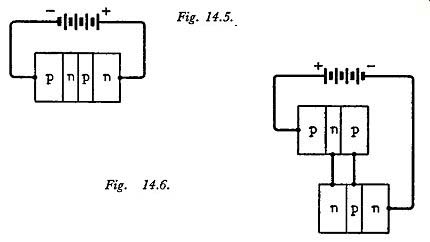
Fig. 14.5. Reverse-biased controlled rectifier

Fig. 14.6. Forward biased rectifier represented as two direct-coupled transistors
PNPN Transistor (Transistor or Controlled Rectifier)
This is a four-layer semiconductor device with a structure of the form shown in Fig. 14.4, which can be represented more simply as in Fig. 14.5. It has two stable states, one in which the resistance is very low (the conductive state) and the other in which the resistance is very high (the non-conductive state). The device can be switched very rapidly from non-conduction to conduction and very little power is needed to bring about this change of state. Thus the pnpn transistor has properties similar to those of a thyratron (gas filled valve) but it is far more efficient; the device is used mainly for switching and power control purposes, e.g., as a controlled rectifier.
To understand the mode of action of the pnpn transistor, the device can be regarded as made up of two triode transistors, one of pnp type and the other of npn type, direct-coupled as shown in Fig. 14.6. Suppose a voltage is applied to the outermost regions of the device, as shown in Fig. 14.5. The polarity of this voltage is such as to reverse bias the two outer junctions of the device: these are the base-emitter junctions of the two triode transistors and both triodes are thus cut off. Very little current can flow through the device and with this polarity of applied voltage the pnpn transistor is in its non-conductive state.
Now suppose the polarity of the applied voltage is reversed: the positive terminal of the supply is now connected to the outermost p-region and the negative terminal to the outermost n-region. The applied voltage now biases the two outer junctions in the forward direction and the outermost p- and n-regions can now act as emitters in the two triode transistors. The centre junction (which is the base-collector junction for both triodes) is reverse-biased and most of the applied voltage acts across this junction.
Let the current which flows through the device be I. This current is carried in the pnp transistor by holes which originate in the emitter region, cross the base region and enter the collector region. The fraction of the total number of holes emitted which reach the collector region is alpha 1, the current amplification factor of the pnp transistor. The fraction (1 - alpha 1) represents the number of holes which combine with electrons in the base region and so fail to reach the collector. The holes which are lost by combination with electrons constitute a current of (1 - alpha 1) I. Now the base region of the pnp transistor is also the collector region of the npn transistor and the electrons which combine with the holes in this region are obtained from the emitter of the npn transistor. Electrons are, of course, the current carriers in an npn transistor and the fraction of those leaving the emitter which arrive at the collector is alpha 2, the current amplification factor of the npn transistor. Electrons reaching the collector thus carry a current of alpha_2 I. If this current equals that carried by the holes from the pnp transistor, we have giving This relationship could also be deduced by considering the inner p-region of the pnpn device. This can be regarded as the collector of the pnp transistor or the base of the npn transistor. By equating the number of holes entering the collector region with the number of electrons lost by combination in the base region, we can again deduce the same result.
This result expresses a limiting condition: provided the sum of alpha 1 and alpha 2 is less than unity, the device is stable even though it is forward-biased. If, however, the alphas total unity ( each equal to 0.5, say) the transistor is on the verge of instability.
Any current amplification occurring in the reverse-biased centre junction (due to ionization by collision, for example) increases both alpha_1 and alpha_2, causing their sum to exceed unity. Equilibrium is then impossible and the current I rises rapidly to a very high value. The process is regenerative because any increase in I causes enhanced ionization, which in turn increases I. Such breakdown occurs naturally if the applied voltage is raised to a high value ( causing a sufficiently intense electric field across the centre junction) and in a controlled rectifier the design might be such that breakdown occurs at an applied voltage of 350 volts.
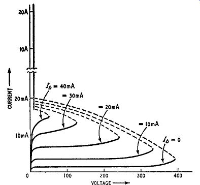
Fig. 14.7. Characteristics of a controlled rectifier.
So far we have assumed that there is no external connection to the inner p- or n-region. Suppose that such a connection is used to apply a negative voltage to the inner n-region (relative to the outermost p-region) that this supplies a current of lb electrons to the device. It is a property of transistors, particularly those employing silicon, that the current gain o: depends on the emitter current, being small for small emitter currents and increasing as the emitter current is increased. The application of a forward bias current to the inner n-region increases the emitter current from the outer p-region, so increasing the current gain alpha of the pnp transistor and the sum of the two alphas. Breakdown now occurs more easily, i.e., at a lower applied voltage than in the absence of external bias. Moreover, by increasing lb, the breakdown voltage can be reduced as low as desired: in practice, the breakdown voltage can be reduced to a few volts only. It is, of course, alternatively possible to control the breakdown voltage by a bias applied to the inner p-region and this has to be made positive with respect to the outermost n-region to reduce the breakdown voltage.
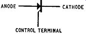
Fig. 14.8. Symbol for controlled rectifier.
The characteristics of the controlled rectifier are given in Fig. 14.7: they are similar to those of a gas-filled triode valve (thyratron). The greatest control power required is only 5 volts at 100 mA: this can control a current of 50 A at 250 volts. With no control signal the rectifier presents a very high resistance and an applied voltage of 350 volts is required to cause breakdown. The resistance then falls to a very low value and currents of up to 50 A can flow through the rectifier with less than 2 volts drop across it. Once breakdown has occurred, the control signal may be removed but the low resistance will remain until the forward current in the rectifier has fallen to a low value. Thus the device can be fired by very short-duration pulses applied to the control terminal. When firing occurs the build-up of current in the rectifier can be very rapid: rise times of 1 microsecond can be achieved.
The controlled rectifier can be used in a.c. power control circuits, in d.c. converters and in voltage-regulated d.c. supply circuits.
The symbol for a controlled rectifier is given in Fig. 14.8.