Introduction
IN this chapter we shall describe a number of miscellaneous applications of junction diodes and transistors which do not properly belong in earlier chapters.
Simple Voltage-stabilizing Circuit
It was pointed out in Chapter 1 that junction diodes could be used as a source of stable voltage and to begin this chapter we shall describe a simple circuit suitable for use where only a small current is required from the stable voltage source.
An example of such a requirement may occur in a transistorized car radio where the supply for the oscillator transistor may require stabilizing against changes in car battery voltage to secure good frequency stability and hence stable tuning. A suitable circuit is illustrated in Fig. 13.1. The junction diode must have a break down voltage equal to the value of the stabilized voltage required ...
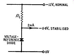
Fig. 13.1. Simple junction-diode voltage stabilizing circuit
suitable for small currents.
... and the value of R1 must be chosen to give an operating point on the nearly-vertical part of the diode characteristic (Fig. 13.2). The diagram represents conditions in the circuit. The load line AB meets the axis at A at a voltage equal to the supply voltage, say 12 volts. AB meets the diode characteristic at B and this point corresponds with the stabilized output voltage. OC represents the voltage drop across the diode and AC the voltage drop across R1. In the chosen example the stabilized voltage is 6.8 volts.
The slope of AB corresponds to the resistance R1 and this clearly may vary within limits (as suggested by the dotted lines AD and AE) without much effect on the value of the stabilized voltage but ...
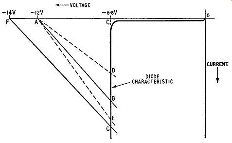
Fig. 13.2. Illustrating the operation of a simple voltage-stabilizing circuit
... it is preferable to choose a value for R1 which keeps the dissipation in the diode well within the maximum value prescribed by the makers. For example if the maximum dissipation is 50 mW we can choose to dissipate half of this, 25 mW, at a battery voltage of 12 volts. The voltage across the diode is 6.8 volts and the diode current must be 25/6.8, i.e., 3.7 mA. This current is supplied via R1 together with the current for the load (the oscillator transistor). If the load current is 2 mA, the total current in R1 is 5.7 mA. The voltage across R1 is 5.2 volts and the required value of R1 is given by R _ 5.2 1
- 5·7 X 10^-3 = 900 ohm approximately
The supply voltage may easily rise to 14 volts when the car dynamo is running. The effect such a voltage rise has on the stabilized voltage is illustrated by the load line FG which is parallel to AB (thus representing the same value of resistance R but meets the axis at F corresponding to 14 volts. FG meets the diode characteristic at G representing a greater diode current than before (point B). The new stabilized voltage corresponds to point G which, because of the extreme steepness of the diode breakdown characteristic is at almost the same voltage as before (point B). The dissipation in the diode is now greater than before the increase in supply voltage and care must be taken to see that the maximum safe dissipation is not exceeded when the supply voltage is at its maximum.
The effectiveness of the circuit depends on the steepness of the diode characteristic which is usually expressed as a slope resistance.
This may be as low as 5 ohms, showing that a change of diode current of 1.0 mA gives an alteration in breakdown voltage of only 5 X 10 = 50 mV.
Voltage-stabilizing Circuit including Transistor and Voltage-reference Diode
The maximum current which can be drawn from a simple voltage-stabilizing circuit of the type described above is limited but larger currents can be obtained by use of a current amplifier in conjunction with a voltage-reference diode. One possible circuit is illustrated in Fig. 13.3. This can be regarded as an emitter follower (analogous to a cathode follower), the base (grid) of which is held at a constant voltage by a junction-diode circuit of the type described above. Such a circuit can provide a current magnification of, say, 50, and, provided a suitable transistor is used, currents of the …
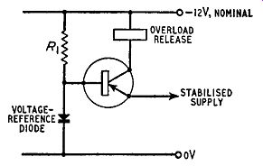
Fig. 13.3. Voltage-stabilizing circuit suitable for supplying large currents
… order of 1 A can be supplied, the input current to the transistor being of the order of 20 mA. The regulation of a circuit of this type can be determined in the following way. Transistors capable of supplying 1 A may require a base-emitter voltage of 500 mV to give this value of emitter current. It follows that the output voltage must change by 500 mV when the current drawn from the circuit changes by 1 A. The effective source resistance is thus 0.5 ohm.
There is a danger that the transistor could be damaged if the output of the regulated supply were short-circuited for this would cause a large current to flow through the transistor causing excessive dissipation in it. The transistor can be protected against such damage by including in the collector circuit a quick-acting overload release device or a resistor which limits the collector current to a safe value.
Junction-diode a.f.c. Circuit
As mentioned in Chapter 1 the capacitance of a reverse-biased junction diode varies with the bias voltage. Such a diode can therefore be used for automatic frequency control and Fig. 13.4 gives a circuit diagram which can be used in an f.m. receiver for this purpose. Not all junction diodes are suitable for this application: for some types the damping due to the resistive component of the diode impedance may be sufficient to reduce the oscillation amplitude to a low value or even to prevent oscillation altogether.
Diodes with very low damping have been developed for use in a.f.c. circuits.
L1C1 is the oscillator tuned circuit and the junction diode is connected across the circuit via the isolating capacitors C2
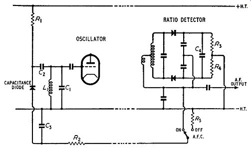
Fig. 13.4. Circuit illustrating the use of a junction diode to give afc.
The diode is reverse-biased from the supply by the potential divider R1R2 and provided that R1 is reasonably high in value, say, more than 40 k!1, the damping of the oscillator circuit by this resistor should not seriously reduce the oscillation amplitude. The capacitance of the diode is effectively in parallel with C1 and alteration in diode bias causes an alteration in oscillator frequency. To obtain a.f.c. the diode bias must be controlled automatically by the degree of mistuning and this can be achieved by returning R2 to the d.c. output of the discriminator. If the discriminator is a Foster-Seeley type, R2 may be connected directly to the detector output provided the connection is made on the detector side of the output coupling capacitor. If a ratio detector is used the connection of R2 is not so straightforward.
The d.c. output of a ratio detector circuit of the type illustrated in Fig. 11.8 has two components: one component varies with tuning and reverses in polarity at the correct tuning point, the relationship between voltage and frequency being substantially linear over a limited frequency range. This is the component responsible for the a.f. output of the detector and is the component required for a.f.c. purposes. The second component is a positive voltage obtained from the long time constant circuit R3R4C4 : this also varies with tuning but has a maximum at the correct tuning point.
To obtain good a.f.c. performance it is advisable to eliminate the second component from the d.c. output of the detector. This can readily be done by earthing the mid-point of the resistor as shown in Fig. 11.4. This gives what might be termed a" balanced" form of ratio detector which gives zero output voltage at the correct tuning point: the d.c. output of such a detector varies with tuning in the same manner as that of a Foster-Seeley discriminator and R2 can then be returned to the detector as shown in Fig. 13.4. The junction diode bias must not be affected by a.f. signals in the detector output and these are therefore prevented from reaching the diode by the capacitor C3 which forms with R2 a potential divider which considerably attenuates all audio frequency signals.
A.f.c. circuits of this type can be extremely effective, reducing mistuning effects by a factor of as much as 10:1. Manual tuning can be very difficult with a.f.c. and it is desirable to have some means of switching a.f.c. off whilst tuning is being carried out. As soon as the wanted signal is tuned in, a.f.c. is switched on to minimize subsequent tuning drift. Fig. 13.4 indicates one method of switching a.f.c. off. The resistor R5 is approximately equal to the d.c. resistance of the ratio detector. Such a resistor is necessary to enable the a.f.c. to be switched off and on when the receiver is accurately in tune, without alteration of the bias across the capacitance diode.
Use of Transistor to increase Relay Sensitivity
Electromagnetic relays enable one or more circuits to be switched on and off by a controlling current much smaller than the controlled current. For example a relay requiring 5 mA of input current can control a circuit carrying 5 amperes.
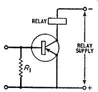
Fig. 13.5. Use of a transistor u, increase relay sensitivity
By use of a transistor as a current amplifier, the sensitivity of a relay can be greatly increased. As we have seen, a common emitter amplifier can easily give a current gain of 50 and by using such an amplifier with the relay mentioned above only 100 µ,A of input current is needed to control the 5-ampere circuit.
A suitable circuit diagram is given in Fig. 13.5. The base of the transistor is returned to the emitter via R1 causing a collector current too small to operate the relay. A small input current causes the transistor to conduct and the relay to operate.
A desirable practical precaution is to connect a diode across the relay winding to prevent generation of large collector voltages across the relay coil when the transistor input is removed and the collector current is cut off. Such voltages can exceed the collector breakdown voltage and can damage the transistor.
The use of a transistor with a relay is a convenient circuit arrangement because the transistor requires no supplies other than that required for the relay and takes up very little space.
D.C. Converters
Transistors are particularly useful in the construction of d.c. converters, units which can be made remarkably compact and which can convert power from a low voltage source (e.g., 6 volts) to a higher voltage (e.g., 120 volts) with an efficiency which can approach 85 percent and is seldom less than 60 percent.
The transistor in such a converter is used as a switch which interrupts the d.c. supply from the low-voltage source to produce alternating current. This is stepped up in voltage by a transformer or resonant circuit to give a high-voltage supply which is rectified and smoothed to obtain the high-voltage output. For high efficiency the power dissipated in the transistor itself must be small.
The power dissipated in a transistor is of course given by the product of the collector current and the collector-emitter voltage.
The power is therefore small when the collector current is nearly zero, that is to say when the transistor is cut off and also when the collector-emitter voltage is nearly zero, that is to say, when the transistor is fully conducting. Thus the design of the d.c. convertor must be such that the transistor is at all times either fully conducting or cut off. This is achieved by using the transistor as an astable relaxation oscillator which generates rectangular waves.
The basic principles of one type of d.c. converter circuit can be illustrated as shown in Fig. 13.6 in which the transistor is shown for simplicity as a switch. When the switch is closed a magnetic field begins to grow in the transformer core. This takes a little time to reach its maximum value and whilst it is still growing a voltage equal to n Vb is generated in the secondary winding where 1:n is the step-up turns ratio of the transformer. The polarity of the rectifier is such that this secondary e.m.f. drives a current through the load. If the switch were left closed the magnetic...
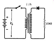
Fig. 13.6. Basic circuit
of one type of transistor d.c. converter.
... field would in time reach its maximum value and become static: there would then be no secondary voltage. However, before this instant is reached, the switch is opened and the magnetic field collapses suddenly, setting up a secondary e.m.f. with a polarity opposite to that set up on closing the switch. This e.m.f. does not cause current to be delivered to the load because the polarity is in the opposite direction to that necessary to drive current through the rectifier.
A simple circuit such as this will behave as a d.c. converter and has the merit of good regulation but the efficiency is low primarily because of the loss of power associated with the e.m.f. generated when the switch is opened. To achieve high efficiency this power ...
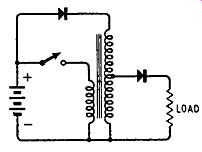
Fig. 13.7. Basic converter circuit
with provision for returning reverse secondary e.m.f. to the low-tension
battery.
... must be put to use and one of the methods used is to return the power to the low-tension source as indicated in Fig. 13.7. By replacing the switch by a transistor we obtain the complete circuit of a d.c. converter shown in Fig. 13.8. The collector and base ...
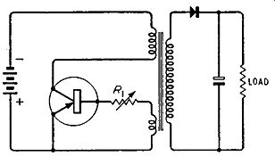
Fig. 13.8. Complete circuit of transistor d.c. converter
... circuits of the transistor are coupled to give positive feedback and consequent oscillation. Considerable feedback is necessary to drive the transistor hard into conduction and cut off. The ratio of the periods of conduction and non-conduction can be controlled by adjustment of the value of the resistor R1, which determines the base bias of the transistor. Frequently d.c. converters of this type (termed the transformer type) employ two transistors operating in push-pull.
In an alternative (ringing-choke) form of d.c. converter, power is delivered to the load during the period of cut off of the switching transistor. As before, the transistor switches the low-tension source across an inductor, thus establishing a magnetic field as before, and then breaks the primary circuit. The e.m.f. generated across the inductor by the collapse of current on breaking the battery circuit causes the rectifier to conduct and thus supplies power to the load.
The circuit diagram is thus similar to that of a transformer converter but employs an inductor instead of a transformer. The ringing choke circuit can be as efficient as the transformer type but the regulation is inferior.
Oscillation frequencies in d.c. converters may lie between 500 hz and 10 khz. If a converter is required to be particularly compact the transformer and smoothing capacitor must be small. This is practicable, provided the working frequency is high, and the tendency is therefore to have high working frequencies in compact converters.
Photo-diode It is shown in Chapter 1 that the current which flows across a reverse-biased pn junction is carried by minority carriers, i.e., by ...
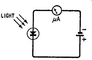
Fig. 13.9. Simple circuit using a photo-diode
... the electrons and holes liberated by breakdown of the covalent bonds of the intrinsic semiconducting material. This current is substantially independent of the reverse bias voltage, provided this exceeds approximately 1 volt, but can be increased by heating the material or by allowing light to fall on it: both give the semi conductor atoms more energy and cause more covalent bonds to break. Where sensitivity to light is undesirable junction diodes and transistors are sealed in opaque containers: if sensitivity to light is required a transparent container is employed.
A junction diode in a transparent container is known as a photo diode and can be used to indicate the presence of light. An obvious form of circuit is that illustrated in Fig. 13.9. The current which flows in such a circuit when the diode is in darkness is due entirely to thermal dissociation of covalent bonds and increases rapidly as temperature rises. It was known as the reverse current in Chapter 1 but in photo-diodes is usually known as the dark current. The ratio of light to dark current thus decreases as temperature rises.
The output power from a photo-diode is limited and amplification is essential if greater power is required, e.g., to operate a milli ammeter or a relay. Amplification can be provided by a transistor direct-coupled to the photo-diode as shown in Fig. 13.10. In this ...
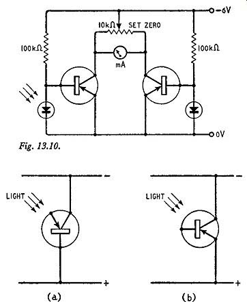
Fig. 13.10. Light-meter circuit employing two photo-diodes and two transistors
Fig. 13.11. Photo-sensitivity of a transistor arranged as at (b) is considerably greater than when arranged as at (a)
... circuit two photo-diodes and two transistors are used in a balanced circuit which largely eliminates the effects of temperature changes and gives a meter reading which depends only on the illumination falling on one of the photo-diodes.
To set up the circuit the two photo-diodes are screened from light and the potentiometer is adjusted to give zero meter reading. When one of the photo-diodes is now exposed to light the meter gives an indication proportional to the illumination and the meter can, in fact, be calibrated in terms of illumination.
Photo-transistors
A photo-transistor may alternatively be used to produce an output greater than is possible from a photo-diode. The mechanism of the amplification inherent in a photo-transistor can be explained in the following way.
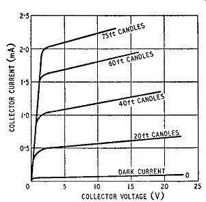
Fig. 13.12. Characteristics of a photo-transistor.
First consider a transistor connected to a supply as indicated in Fig. 13.11 (a). It was pointed out at the beginning of Chapter 6 that the small leakage current Ico which flows in such a circuit arises from dissociation of covalent bonds and increases rapidly as temperature rises. This current also increases if light falls on the transistor because this also breaks up covalent bonds. The leakage current in this circuit is that of the reverse-biased collector-base junction and is of the same order as that of a photo-diode. Such a transistor circuit therefore provides no greater output than is available from a photo-diode.
Now consider the transistor connected to the supply as shown in Fig. 13.11 (b). Chapter 6 shows that the leakage current lc0' for such a circuit is ( 1 + alpha ') times Ico, i.e., is much greater than that of the transistor connected as in Fig. 13.11 (a). It is in fact the magnitude of this leakage current which necessitates the use of protective circuits for bias stabilization in common-emitter amplifiers.
The leakage current may be due to hole-electron pairs released by heat or released by light and thus a transistor used in a circuit arrangement such as that of Fig. 13.11 (b) can produce a considerable increase in collector current when light falls on the base region.
This is illustrated in Fig. 13.12 which gives the collector current collector voltage characteristics for a photo-transistor plotted with ...
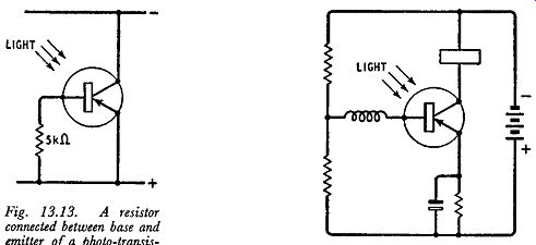
Fig. 13.13. A resistor connected between base and emitter of a photo-transistor
can be used to improve the ratio of light current to dark current
Fig. 13.14. Circuit using a photo transistor with an interrupted light input
... incident light as the parameter. The characteristics are similar in shape to those of a common-emitter amplifier. The curves show that a change of collector current of 0·5 mA can be produced by a change in light input of 20 ft-candles.
If the base circuit of the photo-transistor is open-circuited as shown in Fig. 13.11 (b), the variations in collector current due to temperature changes are considerable. Thus the ratio of light current to dark current is limited and may vary in practice from 100 at 25° C to 10 at 45° C. Provided the photo-transistor is not required to work in surroundings where wide variations in temperature are likely to occur the very simple circuit of Fig. 13.11 (b) may be satisfactory.
Where wide variations in temperature are inevitable it is preferable to have a larger ratio of light current to dark current. This can be achieved by use of a resistor connected between base and emitter as shown in Fig. 13.13. With a resistor of approximately 5 k-ohm the ratio of light current to dark current is now increased to 400 at 25° C falling to 20 at 45° C. There are some applications of photo-electric devices where the light input is " chopped"; this occurs, for example, where the device is used for counting articles moving along a conveyor belt.
A photo-transistor circuit suitable for such an application is illustrated in Fig. 13.14. This employs the potential-divider method (see Chapter 6) of dark-current stabilization but to avoid reduction in light current an inductor is included in series with the base lead to the photo-transistor. To give maximum output this inductor should be parallel-resonant at the frequency of the light variation.