AMAZON multi-meters discounts AMAZON oscilloscope discounts
IN TELEVISION, as in radio, the signal is fundamental. Although in radio the signal represents sound values and in television the signal represents light values, in both cases the information being transmitted is converted into electrical signals. Thus it is to be expected that signal tracing in television receivers will be generally similar to that in radio receivers. For example, the problem of checking the operation of a video amplifier is not essentially different from that of checking an audio amplifier stage since in both instances the same process of amplification of an electrical signal is involved. We do not mean to imply that the procedures are identical but rather to point out that television, as well as radio, deals with the amplification, frequency conversion, detection, etc., of electrical signals, so that television servicing will in general be closely related to radio servicing.
You can readily see that the problems involved in television servicing are more complex than those in radio servicing. This is a natural consequence of the fact that the television signal is exceedingly more complex than the radio signal used in sound broadcasting. Thus the television signal not only must convey information on the light values at each one of the many small elements into which the televised scene is broken down, but the signal must carry the synchronizing information required to reassemble these light values in the proper order. In addition to the complexity introduced by the necessity for supplying the synchronizing information, television receivers are complicated by the presence of other alternating voltages which in a sense can be thought of as signal voltages. In this class can be mentioned the horizontal and vertical deflecting voltages and the comparatively complex circuits associated with the production of these voltages or signals. In the same way, the synchronizing pulses which are required for the proper synchronization of the horizontal and vertical deflection voltages are also signals in a real sense and further add to the complexity of the television receiver. Add to this, the larger number of stages and component parts in the average television receiver, and you can easily appreciate why television servicing is more complex than radio servicing.
In this section we emphasize the part that the signal plays in the proper operation of the television receiver. We shall show how the character of the signal changes as it passes from one stage to another in the receiver and how each stage contributes to the final image which is reproduced on the screen of the picture tube. We shall show how the apparently complex schematic that represents the television receiver is in reality a coordinated scheme in which each part performs a definite function.
Fundamentally, the efficient localization of trouble in a tele vision receiver depends upon a clear understanding of the various types of signals which exist throughout the receiver. It is only when you have acquired this understanding that faulty operation of the receiver can be interpreted in terms of the failure of the signal to have the proper character at one or more points in the receiver. We are here using the term signal in its broader sense to include control voltages and other factors which influence receiver operation. For example, an understanding of the fact that the horizontal deflection oscillator requires a sync pulse signal in order to insure proper timing, at once leads one to look for trouble in the sync (and deflection) circuits in the event that the picture obtained is such that improper timing of the horizontal oscillator is indicated. Again, inability of the brightness control to enable cutting off the beam completely, indicates that some thing is wrong in the bias circuit of the picture tube. Possibly this might be a defective output tube (in the case of direct coupling to the picture-tube grid), but at any rate, the point you should note is that the defect itself or its symptoms provide the clue to the source of the trouble.
The Complete Receiver
In order to show the operation of television receivers let us first examine the general arrangement of stages in a typical receiver. Fig. 10-1 is a block diagram of a typical television receiver especially arranged to show the general character of the signal through the receiver and the function performed by each section.
For convenience we shall assume that the receiver is tuned to the 44-50 mhz channel. In accordance with the standards adopted by the RMA (Radio Manufacturers Association), this means that the frequency of the video carrier is 45.25 mhz (1.25 mhz above the low-frequency end of the channel) whereas the frequency of the audio carrier is 49.75 mhz (0.25 mhz below the high-frequency end of the channel). Both these signals, together with their sidebands, are picked up by the antenna and fed through a transmission line to the input of the r-f amplifier. Essentially the function of the r-f amplifier is the same as that of the r-f amplifier in any super heterodyne receiver-to amplify the signal and to reject unwanted signals in adjacent and other channels. In this case, the r-f amplifier is broadly tuned so that both the video and sound carriers, which are separated by 4.5 mhz, are amplified equally.
After being amplified in the r-f amplifier, both signals are fed to the first detector circuit where the conversion of the signals to the intermediate frequencies takes place. Since there are two radio frequencies, it of course follows that two separate inter mediate frequencies are produced.
In accordance with a proposed RMA standard, and general present practice, the oscillator operates at a frequency 1S.75 mhz above the video carrier frequency. For the channel being received, the frequency of the oscillator in the receiver is thus equal to 45.25 mhz+ 12.75 mhz, or 58 mhz. Since the oscillator frequency is 12.75 mhz above the video carrier frequency, it follows at once that the video intermediate frequency produced is equal to 12.75 mhz. In the same way, the intermediate frequency of the sound signal is equal to the difference between the oscillator frequency and the sound carrier frequency, 58 mhz-49.75 mhz, or 8.25 mhz.
Following the first detector, the sound channel is entirely independent of the rest of the receiver and in practically every detail is similar to a conventional broadcast receiver. Thus the 8.25 -mhz sound i-f signal passes through the sound i-f amplifier (the selectivity of which is broader than usual to minimize the effects of oscillator drift, as mentioned above) and is demodulated at the sound second detector. The avc voltage is supplied in the usual manner to control the gain of the stages in the sound i-f amplifier.
The design of the audio amplifier and the reproducer is also conventional so that no further comment is required.
Returning to the video signal, we have seen that a 12.75-mhz i-f signal is produced by the first detector and that this signal carries the video modulation. As the diagram shows, this signal is amplified in the video i-f amplifier, which usually consists of several stages, and finally reaches the video second detector where the …
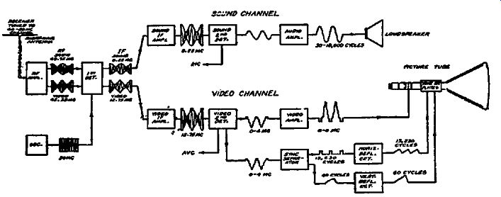
Fig. 10-1. Block diagram of a typical television receiver showing the principal
sections of which it is composed. Note the changes in the signal as it passes
through the receiver.
...signal is demodulated. The video signal recovered at this point is essentially the same as the output of the camera tube so that it contains all the information required to reproduce the picture, and in addition, includes the blanking and sync pulses. The video second detector is followed by the video amplifier which, in terms of a sound receiver, corresponds to the audio amplifier. The function of the video amplifier is to amplify the video signal so that its amplitude will be great enough to "swing" the modulation grid of the picture tube. For the average picture tube this requires approximately 25 volts, peak-to-peak.
Note in the diagram that the polarity of the video signal is reversed 180 degrees for a single stage of video amplification and that the receiver is arranged so that the signal which reaches the control grid of the picture tube has a positive polarity. As a result the synchronizing impulses appear in the blacker-than black (highly negative grid-bias) part of the picture tube characteristic so that the beam is blocked during the retrace part of the line and field sweeps.
In addition to supplying the video signal and the signal which actuates the avc system, the second detector supplies the video signal to the synchronizing separator. The purpose of this separator is to remove the picture component from the complete video signal, and then to separate the horizontal sync pulses from the vertical sync pulses. As is shown, the horizontal sync pulses are arranged to control the timing of the horizontal deflection circuit, while the vertical sync pulses are arranged to control the timing of the vertical deflection circuit.
The power supply is not shown in the block diagram. As a general rule, a single low-voltage power supply is used to take care of all voltage requirements throughout the receiver with the exception of the high-voltage requirements for the picture tube.
The latter, which may include voltages as high as 9000 volts, is supplied by a separate high-voltage power supply which has its own transformer, rectifier and filter.
R-F Circuits
Since the complete television signal consists of a band of frequencies extending over a 6-mhz channel, it is clear that the r-f circuits, including the antenna and transmission line, must be broad enough to pass the 6-mhz band. A sharply tuned antenna system is undesirable because it discriminates against the different frequencies present in the signal and as a result produces distortion.
The characteristics of the r-f circuits in television receivers are the same as for ordinary broadcast receivers. As in any super heterodyne receiver, the function of the r-f circuits is to select and amplify the wanted signals and to reject all other signals. As a general rule, most television receivers do not use an r-f stage but rely on the selectivity of the tuned circuit which feeds the signal from the transmission line to the mixer input to provide the required selectivity and image rejection. In some receivers, however, an r-f stage is provided so that additional gain, selectivity and a higher signal-to-noise ratio are obtained.
In most cases you will observe that the r-f tuned circuits as well as tuned circuits in the i-f amplifier are shunted by resistors of comparatively low value. The function of these resistors is to damp the circuits so that sideband cutting will not take place and so that the complete television signal will be passed. Al though these resistors lower the gain, this reduction in gain must be tolerated in order to broaden the circuits sufficiently.
Without exception all commercial receivers use push-button or switch-controlled tuning rather than conventional continuous tuning with a large variable condenser. This is feasible because the short-wave channels which have been assigned for television are limited in number and do not require continuous coverage as is the case, for instance, in the broadcast band. At the present time the lower channels are most in use and will probably be the only ones in use for some time.
As a general rule, a small vernier condenser is provided to permit a fine adjustment of the tuning. This condenser is placed across the oscillator tuned circuit and compensates for drift in the trimmers and other effects which tend to change the oscillator frequency. No external tuning adjustments are required for the r-f circuits since these are not critical of adjustment.
Oscillator Circuits
As has been previously pointed out, the oscillator in a television receiver beats with both the sound and video carriers of the signal to form two separate intermediate-frequency signals: the video i.f. and the sound i.f. According to present standards, the oscillator frequency for any given channel is 14 mhz above the low frequency end of the channel, which in turn makes it 12.75 mhz above the video carrier and 8.25 mhz above the audio carrier. As a result, the frequency of the signals produced by heterodyning with the oscillator signal is 12.75 mhz for the video i.f. and 8.25 mhz for the sound i.f.
Combination oscillator and mixer tubes are not satisfactory for the comparatively high frequencies at which the oscillator must operate, because of low conversion gain and because these tubes do not oscillate readily at the high frequencies required. For these reasons a separate tube is generally used for the oscillator circuit. The type 6J5 tube is more widely used than any other tube because of its high mutual conductance, low capacitance, and because it oscillates readily at frequencies up to about 120 megacycles.
In the design of oscillator circuits much attention is given to the problem of minimizing frequency drift. Because of the high frequencies at which the oscillator operates, a comparatively small percentage change in the oscillator frequency, such as might be caused by drift, has the effect of spoiling the picture and causing the sound i.f. to drift out of the range of the sound i-f channel.
Although the effect of oscillator drift is minimized because of the comparatively high intermediate frequencies, the problem of oscillator stability and freedom from drift is an important one. In commercial receivers, drift is minimized through proper circuit design and by the use of coils and condensers which are independent of changes in temperature and humidity.
Mixer
As has previously been pointed out, combination oscillator mixer tubes such as are satisfactory at lower frequencies are not satisfactory at frequencies above 40 mhz. It is general practice to use one of the new high mutual conductance tubes in the mixer circuit, such as the type 1852. The 1852 is especially adapted for frequency conversion and provides high conversion efficiency. For proper mixer operation, it is essential that the output of the separate heterodyning oscillator be coupled to the mixer tube and that the mixer receive approximately the same value of voltage from the oscillator on all bands.
Typical R-F, Oscillator, and Mixer Circuits
The circuit shown in Fig. 10-2 is that of the high-frequency section of the Belmont Model X-466 receiver. This receiver does not use an r-f stage but the signal is coupled directly to the grid of the 1851 mixer tube through a double-tuned closely coupled bandpass circuit. This bandpass circuit provides the required selectivity without sacrifice in gain. Five of the assigned tele vision channels are covered, beginning with the 44-50 mhz channel, the highest channel being the 84-90 mhz channel. The three highest-frequency channels are shunted by resistors having a value between 1000 and 2000 ohms in order to obtain the required pass band. These resistors do not have the loading effect that might be expected offhand, since the loading of the input resistance of the tube is itself of the order of 1000 ohms. In addition to improving the gain and selectivity of the input circuits, the tuned primary windings of the input transformers aid in proper matching of the transmission line and in eliminating reflections.
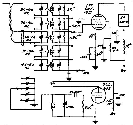
Fig. 10-2. The high-frequency section of the Belmont Model X-466 receiver.
The signal from the oscillator coil is inductively coupled to the mixer input
coil.
These reflections are undesirable because they tend to produce more than one image on the screen of the picture tube.
The oscillator circuit, which uses a 6J5 tube, is conventional in design, with the tank circuit located in the grid circuit. Note the comparatively small value of the grid condenser, 25 mmf. The major portion of the total capacitance in the tank circuit of the oscillator is selected by means of the 5-position switch which is of course ganged with the r-f selector switch. A small vernier tuning condenser across the grid coil provides an adjustment which compensates for small variations due to oscillator drift.
This control appears on the panel and is designated as the tuning control.
A type 1851 tube is used as the mixer tube. This is a pentode having a high mutual conductance, and is similar to the 1852 but has the grid cap on the top. It is used in preference to a 6J7 because it provides higher gain and a higher signal-to-noise ratio.
There is no direct coupling connection between the oscillator circuit and the mixer; the required coupling is provided inductively by placing the oscillator coil close to the mixer input coil.
I-F Circuits
As a result of the action in the mixer circuit, we have seen that two intermediate frequencies are produced and that one of these--the video i.f.-carries the picture signal, while the other one the sound i.f.-carries the sound signal. As in the conventional superheterodyne receiver, it is necessary to amplify both of these i-f signals before they are finally demodulated in the second detectors. These functions are performed by the video i-f and the sound i-f amplifiers. In this section we shall discuss the design of i-f circuits for television receivers and illustrate the principles with circuits taken from typical existing receivers.
Signal Output of Mixer. The frequencies which must be handled by the two i-f amplifiers are illustrated in Fig. 10-3. Let us assume that a signal in the 44-50 mhz channel is being received.
Fig. 10-3. The upper part of this figure shows the make-up of a video signal
in the 44-50 mhz band.
The lower part shows that the same frequency separation is maintained in the i-f signal as in the r-f signal.
In this channel, the video carrier is at 45.25 mhz and the sound carrier is at 49.75 me; the local oscillator frequency, which is 14 mhz above the low-frequency end of the channel, is therefore at 58 mhz (44 + 14). As a result of beating with the oscillator, the video i-f signal at 12.75 mhz (58-45.25) and the sound i-f signal at 8.25 mhz (58-49.75) are produced. It is important to note, as the figure shows, that whereas the video r-f carrier is lower in frequency than the sound r-f carrier, the video i.f. is higher in frequency than the sound i.f. However, the relative placement of the various components of the complete signal is the same in the i-f signal as in the r-f signal. Thus the frequency separation between the two carriers is constant at 4.5 mhz in both cases as is also the separation from the two ends of the channel.
The intermediate frequencies used in television receivers have a number of desirable qualities which are the result of careful planning by television engineers. Thus the frequencies are high enough to give good image rejection; this is especially important because many receivers do not use an r-f stage. At the same time, the video i.f. is high enough so that there is sufficient space for the sidebands and the sound i.f. is high enough so that the sound selectivity is not too sharp. The effect of too sharp selectivity in the sound i-f amplifier is to make tuning critical, to exaggerate the effect of the slightest drift in the oscillator frequency and to prevent adjustment for the best picture detail with out losing the sound signal.
Like any other superheterodyne, television receivers are subject to interference due to pickup by the antenna of frequencies within the range of the i-f amplifier. In the case of broadcast receivers, such interference shows itself in the form of squeals, code signals, and general distortion. Similarly, in the case of television receivers such pickup may distort either the picture, the sound, or both, depending upon the frequency of the interference. The range of intermediate frequencies between 8 and 14 mhz has been especially chosen to minimize i-f interference; the fact that the amateur bands lie outside of this range is of considerable assistance in this respect.
Sound I-F Channel. It is the function of the sound i-f amplifier to separate the sound component of the i-f signal from the video component and to amplify this signal before it is demodulated at the sound second detector. Because of the comparatively high frequencies involved, however, the design of a television sound i-f amplifier is somewhat more difficult than that of the conventional i-f amplifier in a radio receiver. Thus there is a greater tendency toward regeneration and more attention must be paid to stray wiring and tube capacitance.
The bandwidth which must be passed is comparatively small and does not present the same problem as does the video i-f amplifier. Actually, of course, a bandwidth of from 10 to 20 khz is sufficient to transmit all the frequencies present in the audio signal. However, in practice, the bandwidth of the sound i-f amplifier is made approximately 100 khz. Primarily this larger bandwidth is necessary to allow for normal drift in the frequency of the oscillator. The significance of this is that if the bandwidth of the sound i-f amplifier were held to 10 khz, then a change of 10 khz in the oscillator frequency would cause the sound signal to drift completely out of the range of the sound i-f amplifier. however, a change of 10 khz, in an oscillator operating at a frequency of the order of 60,000 khz and up, represents a frequency drift in the oscillator of only one part in 6000, whereas in practice it is not possible to design receiver oscillators which will have a reliable frequency stability of better than one part in 1000. Therefore, instead of resorting to voltage regulation and expensive design to prevent oscillator drift, the bandwidth of the sound i-f amplifier is intentionally made about ten times as great as that required for the sound modulation, thus allowing for reason able drift in the oscillator. Assuming that the receiver is initially tuned to the center of the sound i-f amplifier, a drift in the oscillator frequency as high as 25 khz will not cause any appreciable change in the quality of the audio signal. This is illustrated in Fig. 10-4, which shows that the effect of a change in the frequency of the oscillator is merely to shift the location of the sound signal within the band passed by the sound i-f amplifier.
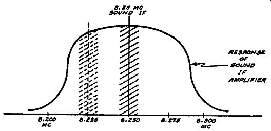
Fig. 10-4. The frequency response of a typical sound i-f amplifier. The dotted
signal shows that the sound signal can be detuned appreciably without falling
out side the pass band of the amplifier.
Although the bandwidth of approximately 100 khz is sufficiently great to compensate for normal oscillator drift, this bandwidth is still small enough so that the receiver can be tuned by listening to the sound accompanying the picture. At the same time there is enough latitude so that the tuning can be varied slightly in order to improve the detail of the picture without losing the accompanying sound signal. Although we shall see later that a special type of avc circuit is required in the video i-f amplifier, the avc circuits used in the sound i-f amplifier are conventional.
Video I-F Circuits
The design of the video i-f amplifier is more complicated than that of the sound i-f amplifier because of the wide band of frequencies which the video i-f amplifier must pass. Thus the video i-f amplifier often must handle frequencies extending from approximately 8.7 mhz to 14.0 mhz, a range of over 5 mhz. Not only must the amplifier have an almost flat response over this range, but at the same time it must reject interfering signals close to the edges of the pass band.
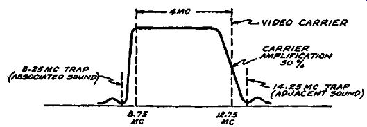
FIG. 10-5. The overall frequency response of a typical video i-f amplifier.
Note that the carrier receives only 50% of the maximum amplification.
The use of the so-called vestigial sideband transmission, in which all of one sideband and a small portion of the other side band are transmitted, makes it necessary for the selectivity of the i-f amplifier to depart from the uniform selectivity which might at first be expected. To avoid overemphasis of the lower video frequencies, which receive contributions from both the upper and lower sidebands, the selectivity of the i-f amplifier is designed to have a sloping characteristic in the neighborhood of the video i-f carrier at 12.75 mhz. This is illustrated in Fig. 10-5 which shows a typical overall selectivity curve for a video i-f amplifier. The amplification which the i-f carrier receives is only 50% of the maximum amplification received by the upper sidebands and the lower sidebands, which are only partially transmitted, also do not receive the full amplification. In this way overemphasis of the lower video frequencies is avoided by shaping the overall selectivity so that the contribution of the lower sideband plus the contribution of the upper sideband is equal to the gain for the higher video frequencies. Since the upper video frequencies receive contributions only from the one sideband, the selectivity, as Fig. 10-5 shows, is such that the full gain is received by these frequencies.
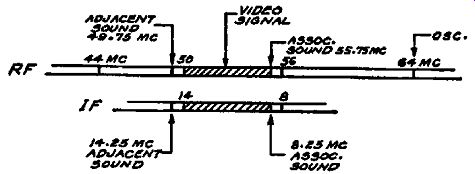
Fig. 10-6. The sound signal of the associated channel at 8.25 mhz and the
sound signal of the adjacent channel at 14.25 mhz are both close to the edges
of the video band. Traps are provided to prevent interference from these signals.
If video frequencies up to a maximum of 4 megacycles are to be received, which is usual for the higher-priced sets using large picture tubes, then the i-f amplifier should cut off at about 8.75 mhz (12.75-4.0). Since the sound i-f carrier is located close by, at 8.25 mhz, it is necessary that this cutoff be sharp in order to prevent the sound carrier and its sidebands from causing interference with the video signal. In practice this rejection of the sound carrier is secured by the use of rejection or trap circuits which generally are part of the video i-f coupling transformers.
In addition to rejecting the sound i-f carrier of the associated channel at 8.25 mhz, it is desirable that the i-f amplifier have a sharp cutoff at the high-frequency end of the band. This is required in order to prevent the sound signal on the lower adjacent television channel from getting through the video amplifier. Because of the reversal of high and low frequencies which takes place in the mixer, the sound carrier of the lower adjacent channel will beat with the oscillator and cause an interfering signal which is located 0.25 mhz above the edge of the channel, at 14.25 mhz. These frequency relationships ·just described are shown in Fig. 10-6. A trap of the same general type as that used to reject the 8.25 mhz carrier is used to reject possible interference from the adjacent sound carrier at 14.25 mhz.
The maximum gain which can be obtained in a video i-f stage is considerably lower than that in an ordinary broadcast i-f stage because of the wide band of frequencies which must be passed and because of the high carrier frequency. This is true even where high mutual conductance tubes of the 1851 series are used, so that it is not unusual for as many as five separate stages to be used in the video i-f amplifier.
The transformer design is especially complicated in video i-f amplifiers because of the wide pass band of from 2.5 to 4.0 mhz which must be obtained. To obtain close coupling so as to increase the pass band, direct coupling of the primary and secondary windings by means of a common inductance is often used.
Loading of the tuned circuits with resistors so as to broaden the circuits is very common and will be found in practically all the circuits. Video i-f transformers are further complicated because the rejector circuits for the associated and adjacent sound channels are often an integral part of the interstage coupling trans formers. Because of the comparatively high frequencies, the only capacitance used to tune the circuits is often that of the wiring and tube capacitance so that no condenser as such appears on the schematic. Nevertheless this capacitance forms a resonant circuit with the related windings of the transformer and should be taken into consideration. Since the wiring capacitance is an important part of the total circuit capacitance, it is important that no changes be made in the wiring when servicing is required.
Avc is often used in video i-f amplifiers, but as will be explained later under "AVC Circuits," the manner in which the avc voltage is produced differs from that in radio receivers and in the sound i-f amplifier.
Video I-F in Andrea Model 1F5. In the Andrea Model 1F5 receiver, shown in Fig. 10-7, the video i-f amplifier employs two stages of amplification both of which use type 1852 tubes. In order to separate the sound i-f part of the signal from the video part, a separate secondary circuit LS-CB is tuned to 8.25 mhz so that the sound i-f signal appears across this circuit. The sound i-f signal is fed directly to the sound i-f channel which is conventional and requires no further comment.
The video component of the i-f signal is developed across LS. No trimmer condenser is used on this winding and the circuit is heavily loaded by the 6000-ohm resistor in order to pass the required band of frequencies. The video signal is applied directly to the grid of the type 1852 tube used in the first i-f stage. To obtain negative feedback and the increased stability which it makes possible, an unbypassed 70-ohm resistor is placed in the cathode circuit. The other end of this resistor is connected to a variable resistor--the "contrast control"--by means of which the gain of the i-f stage is controlled. Since no avc is used, the control grid is returned directly to ground. The band of frequencies passed by this amplifier is approximately 2.5 mhz; this pass hand is generally considered to provide sufficient detail for the small picture tube used with this receiver.
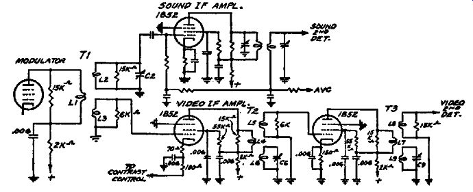
Fig. 10-7. The video and sound i-f amplifiers in the Andrea Model 1F5 receiver.
The signal is coupled to the grid of the second i-f tube by means of the transformer T2. The windings L4 and L5 of this transformer function as the primary and secondary windings of the interstage transformer and are loaded by means of the 15,000~ ohm resistor across the primary and the 6000-ohm resistor across the secondary. The only capacitance used to tune these windings is the tube and circuit capacitance.
The third winding L6 is tuned to 14.25 mhz by means of the trimmer CB and eliminates possible interference from the sound carrier of the lower adjacent television channel, as was previously shown in Fig. 10-6. This circuit acts as a trap by absorbing all the energy in the neighborhood of 14.25 mhz so that it is not passed on to the grid of the following tube.
The second i-f stage feeds directly into the video i-f second detector through the transformer T3 which is similar to T2. The circuit L9-C9 is likewise tuned to 14.25 mhz so that it acts as a trap circuit for this frequency.
No avc is used in the video i-f amplifier in this receiver and accordingly the grids of the two i-f tubes are returned directly to ground. The gain is controlled by means of the "contrast control" which varies the bias of both the first i-f stage and the first detector stage.
Video Second Detector Circuits
In a radio receiver the second detector rectifies the i-f signal and as a result the audio signal corresponding to the variations in the carrier is recovered. In the same way, the video second detector in a television receiver rectifies the video i-f signal and as a result the video signal corresponding to the variations in the amplitude of the carrier is recovered. This video signal is of course that produced by the camera tube and contains in addition the pulses required for synchronization.
Generally speaking, video second detectors are similar to the second detectors of the diode rectifier type used in radio receivers and discussed in a previous section. However, because modulating frequencies as high as 4 mhz (in the larger receivers) must be passed, a lower value of load resistance is used in order to prevent the attenuation of the higher video frequencies. The value of load resistance generally used is of the order of 2500 ohms; on the other hand, the values used in radio receivers are of the order of 250,000, or approximately 100 times as great. Because of the low value of diode load resistance, receivers are generally designed so that the signal level at the second detector is approximately 5 volts or more. This minimizes distortion due to the curvature of the diode characteristic, which is more pronounced when low values of diode load resistance are used.
Video Second Detector in DuMont Models 180-183. The video second detector circuit used in the DuMont Models 180-183 receivers is shown in Fig. 10-8. A full-wave rectifier circuit is used so that both halves of the signal are rectified. Since the cathodes are connected to the ends of the center-tapped secondary, each diode will draw current when its cathode is negative with respect to ground (the diode plates both return to ground through the 3000-ohm load resistor). As a result the current flow through the load resistor will be in the direction shown. Thus when a video signal is applied to the primary of the transformer, the plate end of the load resistor will become negative in proportion to the ...
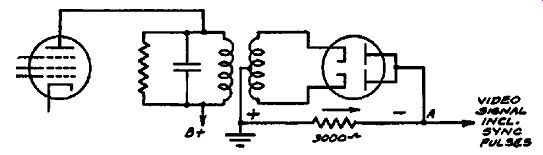
Fig. 10-8. The video second detector circuit in the DuMont
Models 180-183. A full-wave rectifier circuit is used.
... amplitude of the carrier. When the carrier amplitude is greatest, as it is for the sync pulses, the greatest negative voltage will be produced at A. The various shades of white and gray in the signal will produce lesser values of voltage at A, zero voltage of course corresponding to whitest white. In accordance with the definition of signal polarity, the video signal produced at A is said to have positive polarity.
It is worth while noting that if the diode plates, instead of the cathodes, had been connected to the ends of the coil, then the polarity of the video signal would have been reversed. As we shall see in the discussion of video amplifiers, whether or not the diodes are connected to give a signal of positive or negative polarity depends upon the number of stages in the video amplifier. The controlling factor is that the amplified signal which is finally applied to the grid of the picture tube must of course have a positive polarity since a more positive voltage on the grid produces a brighter spot on the screen of the tube.
Video A VC Circuits
Although the ultra-high frequencies used for television are not subject to fading of the same type as that found in the high and medium radio frequencies, the signal strength may still vary because of swinging of the antenna or the presence of automobiles and other moving objects. Since these variations will cause a change in the contrast of the picture being received, they are undesirable and can be avoided if the receiver is equipped with ave. The use of avc also simplifies the design of both the video gain control circuit and the sync separating circuits because it assures the maintenance of a constant signal voltage at the video second detector.
In the conventional avc circuits used in radio receivers, the control voltage is produced by rectifying the carrier and as a result the control voltage is proportional to the average value of the carrier. Because the average value of the carrier in ordinary broadcasting does not change during modulation, it is a measure of the signal strength and hence can be used to control the gain of the receiver.
In television this same system cannot be used because the average value of the video carrier is dependent upon the average illumination of the scene being televised. Thus if the average background of the scene is white, then the average carrier amplitude will be small; on the other hand, if the average background is dark, then the average carrier amplitude will be large. (The above conditions are of course only true for negative modulation which is standard for this country.) Obviously, then, we cannot use the average amplitude of a video signal to obtain the necessary d-c control voltage, because such a control action would vary the gain of the amplifier in accordance with the average back ground illumination and as a result produce distortion.
However, although the average value of a video signal does not remain constant, the peak value always has the same fixed value regardless of the percentage of modulation or the average illumination of the scene. For this reason the peak value of the carrier serves as a convenient reference to establish the strength of the carrier and is the basis of operation of video avc circuits. This peak value is transmitted at the end of each line, that is, 13,230 times in every second, and thus it is available at regular intervals which are frequent enough to make possible the production of an automatic control voltage.
It is of interest to note here that one of the important reasons for the use of negative rather than positive modulation is that only in negative modulation is this regular succession of peak pulses available for avc purposes. The design of avc circuits where positive modulation is used, is considerably more complicated; for positive modulation the peak values of the signal are not fixed but depend upon the brilliance of the scene being televised.
Satisfactory operation in the smaller and less expensive receivers is often secured without the use of a separate avc system in the video channel. In these receivers, relatively few video i-f stages are used so that the problem of manual gain control is not so difficult. In addition, the first detector is often controlled by the avc voltage produced in the sound channel, so that some degree of automatic control is provided. Since the video and sound carriers are close to each other, they undergo approximately the same variations in transmission from the transmitting antenna to the receiving antenna, but in general these variations are not sufficiently alike to permit the use of sound avc voltages on all the video stages.
Video AVC Circuit in the RCA Model TRK-12. The video second detector and avc circuit used in the RCA Model TRK-12 is shown in Fig. 10-9. When a signal is being received, full-wave rectification takes place in the 6H6 and as a result the demodulated video signal is produced across the 4000-ohm load RJ,5 in series with the peaking coil L39. The polarity of this signal is indicated by the insert wave which shows that point B of the load is positive with respect to point A; B can be considered as being at a fixed reference voltage since it is tied down to -33 volts through the filter resistor R47.
The circuit used to obtain the avc voltage from the signal across AB is essentially a peak voltmeter using one section of the 6F8-G tube as a diode. As the circuit shows, the grid is used as the diode plate and is connected directly to point B; the cathode is bypassed to ground by a 1-mf condenser C54 and is returned to A through a 470,000-ohm resistor, R46.
During the sync intervals, the grid of the diode is highly positive with respect to its cathode so that a current flow takes place through R46 and a positive change is stored in C54, Because the sync pulses are repeated rapidly, 13,230 times per second, this charge is continually replenished and C54 remains charged to the peak value of the video signal. If, for example, we assume a 10 volt peak signal, then point C would charge up to a potential 10 volts greater than that at point A or -23 volts (-33 + 10).
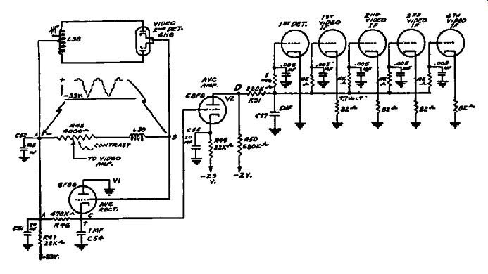
Fig. 10-9. The avc circuit in the RCA Model TRK-12 receiver. The voltage
developed across C54 is amplified by the direct-coupled triode and controls
five stages.
Since the voltage produced in this way is proportional to the peak value of the carrier, it is a suitable measure of the signal level at the second detector. However, its polarity must be reversed in order that an increase in signal input will produce a more negative rather than a more positive control voltage. This reversal of polarity is effected by means of the second section of the 6F8-G which is used as a d-c amplifier.
This tube receives its plate voltage through a 680,000-ohm load resistor R50 which is 2 volts negative with respect to ground.
Since the cathode is returned to -23 volts on the bleeder, the net plate voltage with no input signal is equal to 21 volts (-2 + 23). The grid bias is equal to the voltage at the grid minus that at the cathode or -10 volts (-33 + 23). When no signal is present this value of bias is so great that the cathode current is completely cut off and as a result the voltage at point D is equal to -2 volts. This is the minimum bias with no signal and in combination with the drop of 0.7 volt across the 82-ohm cathode resistor of each of the controlled tubes, provides a net bias of 2.7 volts for each of the video i-f tubes.
On the other hand, when a signal is being received, C54 charges up positively to the peak value of the signal and this positive voltage is applied to the grid of the avc triode amplifier. If the signal is strong enough, the plate current will increase, the voltage drop across R50 will increase, and point D will become more negative than -2 volts. The amount of negative voltage produced at point D is proportional to the strength of the signal and hence the voltage is available for ave.
A delayed avc action is secured because the negative bias of 10 volts, which exists with no signal, drives the grid of the avc amplifier tube considerably beyond cutoff. Thus the signal level must reach a certain minimum value before the plate current will flow and the avc voltage be produced.
In addition to the delay action, the fact that five stages are controlled results in a very effective avc action which maintains the signal level at the second detector essentially constant.
Video Amplifiers
In the same way that the audio signal in a radio receiver requires amplification before it has sufficient power to drive the speaker, so the video signal in a television receiver requires additional amplification following the video second detector before it has sufficient amplitude to swing the grid of the picture tube.
This amplification is supplied by the video amplifier which works between the video second detector and the grid of the picture tube.
The problems associated with the video amplifier, like most television problems, are considerably more difficult than the corresponding problems for a radio receiver. Thus the video amplifier must amplify uniformly frequencies ranging from a few cycles to frequencies as high as 2 to 4 mhz. Whereas phase shift is not important in an audio amplifier, in a video amplifier all the frequencies in the signal must take the same time to pass through the amplifier from input to output. This is important because distortion of the waveform, and hence of the picture, is produced when the different video frequencies do not all take the same time to pass through the amplifier. This type of distortion is illustrated in Figs. 10-10 (a) and (b) which show the difference in waveform produced when a 3000-cycle wave is retarded half a cycle in passing through the amplifier. That the uniformity of time delay plays an important part can be seen from the fact that it takes only approximately seven one-millionths of a second for the cathode-ray beam to move one inch across the screen of the picture tube. Thus even a small non-uniformity in time delay can cause serious distortion of the image.
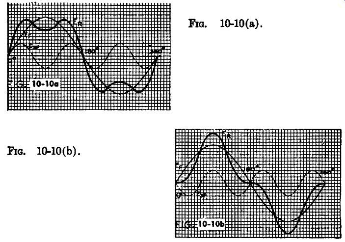
Fig. 10-10(b). The resultant wave E_r is distorted when the phase of the third
harmonic E8 is shifted by a half cycle. Compare with E_R shown in (a) above.
Fig. 10-10(a). The resultant wave E_r is obtained when a 1000-cycle sine wave E_r is combined with a 3000-cycle sine wave E_R which is in phase with the fundamental.
The video amplifiers being used in television receivers now on the market have successfully met the problems outlined above.
By using low values of load resistance, the shunting effect of tube and circuit capacitances has been minimized and the upper frequency limit extended. Fig. 10-11 shows how the use of a low value of plate load resistance, although it lowers the maximum amplification obtainable, makes possible a more uniform gain over a wide range of frequencies. The sacrifice in gain accompanying the use of low values of load resistance has been partially compensated for by the use of the new high mutual conductance tubes which provide approximately three times as much amplification for a given value of load resistance, as was previously possible with the older tubes.
The most common method for obtaining uniform gain is to use so-called "peaking coils" in series with the plate load resistor.
These are small inductances of the order of 100 micro-henries, which are resonated with the tube and wiring capacitance near the high-frequency limit of the video amplifier. Peaking coils permit higher values of plate load resistor for a given uniformity of amplification, and consequently make possible reasonably high gains per stage.
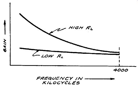
Fig. 10-11. The use of a small value of load resistance provides a more uniform
gain over a wide range of frequencies, although the maximum gain is decreased.
In most video amplifiers, filter resistors and condensers are used in the plate and screen leads to provide low-frequency compensation for both gain and time-delay. These filter resistors and condensers are more critical in value than they are in a radio receiver where the primary purpose is to reduce hum and prevent circuit interaction through the common power supply. For this reason, whenever replacement becomes necessary, the resistors and condensers should be replaced with the correct value. Al though a larger plate filter condenser, for example, will cause no harm and may even do some good in reducing hum in a radio receiver, the same procedure followed in a video amplifier may cause serious distortion of the picture.
Average Brightness and D-C Restorer Circuits
In discussing the video signal, we can look upon this signal as containing a series of voltage values each of which correspond to a particular value of light intensity in the televised image. We can consider that in the same way that light values can be reckoned from black as a reference level, so a particular voltage value can be assigned to black and then each light value represented electrically by assigning a higher ( or lower) voltage to the signal, depending upon the brightness of the light value at the scanned area. This method of looking upon a video signal is shown in Fig. 10-12 (a), in which it is clear that all light values are with reference to the black level-which is taken as the zero voltage axis.
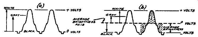
Fig. 10-12. The light values in a video signal can be reckoned in two ways:
In (a) the various light values are described with reference to the black level,
whereas in (b) the same light values are described with reference to the average
brightness of the signal.
Insofar as video amplifier operation is concerned, the important thing about Fig. 10-12 (a) is that it shows that a video signal is inherently a pulsating d-c voltage. In other words (as in the case of a rectified a-c voltage which is also a pulsating voltage) all the light values are represented by electrical values on one side of the zero-voltage axis. The video signal must therefore contain both a d-c and an a-c component in the same way that a rectified a-c voltage representing the output of a power supply contains a d-c component-the d-c voltage of the power supply, and an a-c component-the hum ripple of the power supply.
Physically what does it mean to say that a video signal contains a d-c as well as an a-c component? Actually it is only another way of looking at the signal, as Fig. 10-12 (b) clearly shows. In this figure we describe the signal by saying that the light values are represented by fluctuations in both directions from an average level which we can call the "average brightness," or the "picture background." Thus instead of describing the light value at any point in the scene by stating how much brighter it is than black, as in (a), in (b) we accomplish exactly the same thing by stating how much brighter or blacker is the particular light value than the average brightness. In (a) we use the black level as the reference level whereas in (b) we use the average brightness as the reference level.
Electrically speaking, the average brightness level represents the average value of the video signal or in other words the d-c component of the signal. On the other hand, the fluctuations in the signal on either side of the average brightness level, which is electrically the a-c axis of the signal, represent the a-c component of the signal. An important characteristic of the average bright ness or a-c axis is that the area between the positive part of the cycle and the a-c axis is equal to the area included between the negative part of the cycle and the same a-c axis. This is shown in Fig. 10-12 (b), where it can be seen that area 1 is equal to area B + area 3.
From the preceding it will be clear to you that proper operation of the picture tube requires that both the d-c and a-c components of the video signal be passed by the video amplifier. For if only the a-c component reaches the grid of the picture tube, then the picture tube will have information only on the fluctuations in light values with reference to the average brightness level but it will have no information whatsoever on the value of this average brightness level. Thus the picture cannot be reproduced accurately since the same variations (represented by the a-c component) might be superimposed on say either a dark or light background of any shade. The average brightness, or the d-c component of the video signal, must be present before the picture can be reproduced.
D-C Restorer Circuits
Unfortunately it is not possible to transmit the d-c component of any signal without using a direct-coupled amplifier. However, the use of direct-coupled amplifiers is not practical in television receivers because of their comparative instability and high cost.
For this reason, television engineers have developed circuits which make possible the use of conventional a-c amplifiers with con denser coupling and at the same time provide for the restoration or re-creation of the d-c component after the a-c component has been amplified by itself.
It will be helpful at this time to consider several video signals which have different values of average brightness and to describe the action which takes place when these signals pass through an amplifier which employs a blocking condenser as a coupling element between stages. It is because of the presence of the blocking condenser that only the a-c component is passed and that the d-c component is lost.
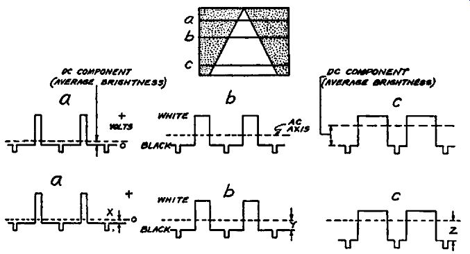
Figs. 10-13 (top), 10-14 (bottom). Fig. 10-13 shows the video wave reduced
when two lines are scanned at a, b, and c, of the white triangle on a black
background. Since the black level is the same for all three cases, this signal
contains the d-e component. Fig. 10-14 shows the same signal after it has been
passed through an a-e amplifier so that the d-e component has been lost.
In Fig. 10-13 the picture being scanned is a white triangle on a black background, with the vertex of the triangle near the top.
Part (a) shows two lines scanned near the top of the picture; part (b), near the middle of the picture; and part ( c), near the bottom. Thus (a), (b) and (c) represent three sections of the picture where the average brightness is low, medium, and high respectively. Fig. 10-13 can be said to represent the signal as it is at the output of the camera tube or as it is recovered at the video second detector. Of special importance is the fact that all the blacks are lined up so that the d-c component of the signal is represented in all cases. Note that the d-c component, like the average brightness which it represents, is successively larger in (a), (b), and (c).
Now what happens to this signal when it is passed through an a-c amplifier which contains coupling condensers and therefore will not pass the d-c component? This is clearly illustrated in Fig. 10-14 which shows that the blacks are no longer lined up, but instead the separate average-brightness or a-c axes are all lined up. In other words, when the d-c component is lost, only the fluctuations on either side of the average brightness are transmitted and this axis must of necessity be the zero voltage axis in all instances because no d-c component can get through the amplifier.
Having investigated the video signal both with and without the d-c component, let us now examine the manner in which the picture tube is affected by the presence or absence of the d-c component. In Fig. 10-13, we see that black in every case corresponds to the same definite voltage value and that is also true for white and every intermediate shade between black and white.
Thus when the voltage of Fig. 10-13 is applied to the grid of the picture tube, the picture will be reproduced without any distortion.
This, however, is not true of the signal in Fig. 10-14, from which the d-c component has been removed. Black no longer corresponds to the same value in all instances, but instead the signal voltage associated with black takes on a value which is entirely dependent upon the average brightness of the strip being scanned. In the same way, this figure shows that white, and in fact every intermediate shade as well, has a different voltage value which is also dependent upon the average brightness of the strip being scanned. A little reflection will show you that this gives rise to serious distortion because the same light value in different parts of the picture does not correspond to the same voltage value in the signal. Thus, for example, the grid of the picture tube receives a different voltage for the same shade of gray in (a), (b) and (c) of Fig. 10-14 and as a result this shade is reproduced differently in the three instances.
In order to remove this source of distortion, it is apparent that the average brightness or the d-c component must be restored. At first glance this seems impossible, for how can the d-c component be restored after it has once been lost in the video amplifier? As a matter of fact, it is generally not possible to restore the d-c component of a pulsating wave after the d-c component has been lost in transmission, because no information relative to the d-c component is contained in the a-c component; the two are entirely independent of each other. Fortunately, however, the sync pulse is transmitted at the end of each line, and the pedestal on which the sync pulse stands corresponds to a definite black reference level. These facts make it possible to restore the lost d-c component. Thus to restore the d-c component to the signal of Fig. 10-14 it is only necessary to modify the signal so that all the synchronizing pulses are lined up. When this is done, the signal in Fig. 10-14 is exactly the same as that in Fig. 10-13 and the d-c component has been completely restored.
The solution of the problem depends upon finding this varying d-c voltage and adding it to the signal. This is accomplished in a very simple manner by using a diode to rectify the "black" half of the a-c video signal (which contains the sync signal) and in this way the required voltage is produced. Thus in Fig. 10-14 at (a) this rectification produces the voltage x; at (b) it produces the voltage y; and at ( c) it produces the voltage z. In general, the addition of this varying d-c voltage lines up all the pedestals to produce the original signal (Fig. 10-13) with the d-c component restored.
Basic D-C Restorer Circuit
In Fig. 10-15 we show a straightforward circuit which is used to restore the d-c component in the video signal before the signal is applied to the control grid of the picture tube. The video signal is developed across the 3000-ohm plate resistor R1 and fed to the control grid through an 0.1-mf coupling condenser C1. As the sketch shows, the signal has the required positive polarity both at the plate of the video amplifier and the grid of the picture tube. However, the d-c component is not present at the plate side of C1, whereas the diode circuit shown in heavy outline has restored the d-c component on the grid side.
Let us see just how the diode circuit restores the d-c component.
Considering the series circuit composed of the video voltage across R1, the .005-mf condenser C2, and the diode in shunt with a 1-meg resistor,-we can see that the following takes place: On the positive half of the cycle the cathode of the diode is swung positive with respect to its plate so that no current flows in the diode circuit. On the negative half of the cycle, however, the cathode is swung negative with respect to the diode plate, and current flows in the diode circuit through RS. It is this current flow which charges Cf and makes the cathode end of RS positive, and as a result provides the d-c restoring bias.
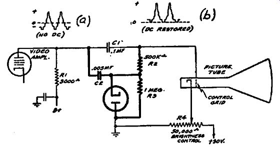
Fig. 10-15. The heavy outline shows a typical d-o restorer circuit which
replaces the d-c component in the video signal before it is applied to the
grid of the picture tube.
Note that the d-c voltage across R3 satisfies all the conditions required to line up the sync pulses so as to restore the d-c component. Essentially the action in the diode circuit is such that the negative part of the video wave is rectified and that the diode current charges Ct positively to a value equal to the amount by which the sync pulses in Fig. 10-15 (a) are depressed below the a-c axis. Since the grid of the picture tube is returned to this d-c voltage through the 50,000-ohm resistor Rf, the d-c voltage is added to the video signal at Fig. 10-15 (a) and "raises" the pedestal so that it lies along the zero-voltage axis, as shown at Fig. 10-15 (b). Now suppose, as in Fig. 10-14 (c), that the average brightness is higher than that shown at (a) in Fig. 10-15. This results in the pedestal being more negative with respect to the a-c axis, so that the diode produces a more positive voltage which again raises the pedestal to the same zero-voltage axis as at (b) in Fig. 10-15.
Thus the action is entirely automatic so that all the pedestals are lined up at the grid of the picture tube, regardless of the value of the average brightness.
It is important to understand that the voltage produced at the cathode varies constantly throughout the scanning and that its value at any time depends upon the average brightness of the portion of the picture being scanned at that particular time. The time constant (RC) of the diode circuit is designed so that CB in Fig. 10-15 will not discharge appreciably during the interval between successive sync impulses. At the same time, the time constant is sufficiently small so that when the average brightness changes, the condenser is able to change its charge rapidly enough to respond to the new conditions.
Insofar as the grid of the picture tube is concerned, it receives the a-c component of the video signal through C1, and only the d-c component through R2. Although the a-c component is also present at the cathode of the diode, R2 acts as a filter resistor to prevent that portion of the video signal present at the cathode from reaching the picture-tube grid through R1.
Brightness Control
We have just seen how the d-c restorer circuit automatically lines up all the sync pulses so they are at the same voltage level.
For correct operation of the picture tube, the bias on the picture Fig. 10-16. The effect of variation in the bias voltage on the brightness of the image.
tube must be so adjusted that these aligned pedestals occur at the cutoff or black level. The sync pulses will then lie in the blacker-than-black region and the various shades of gray and white will be reproduced correctly.
Fig. 10-16 shows the illumination characteristic of a picture tube and the manner in which the brightness of the scanning spot depends upon the bias voltage on the control grid. Referring again to Fig. 10-15 you can see that the cathode of the picture tube is returned to a potentiometer which makes it possible to vary the bias voltage from 0 to 90 volts.
When the bias is highly negative, the tube is cut off and the spot intensity is zero. As the bias becomes more positive, the intensity of the spot increases. For correct operation, the bright ness control should be adjusted manually so that the pedestals occur at the black or cutoff points. Once the brightness control has been set, the d-c restorer circuit automatically keeps the pedestals in alignment so that no further adjustment is required.
Grid Leak-Condenser Restorer
Another type of d-c restorer circuit which is very widely used is shown in Fig. 10-17. In this circuit the output video amplifier tube is operated at zero bias and the grid-cathode elements are used as a diode to insert the missing d-c component. To prevent the loss of the newly restored d-c component which would occur if condenser coupling were used in coupling the plate to the picture tube, the plate is coupled directly to the picture tube grid.
From the explanation already given of the process of d-c restoration, it is easy to understand how circuits of this type operate.
The waveform of the video signal on the left side of C1 is shown at (a); at this point the signal has a negative polarity and of course the d-c component is missing. When this a-c signal is impressed on the grid of the output tube through C1, the positive parts of the video cycle (including the sync pulses) place the grid positive with respect to its cathode so that grid current flows through R1. The direction of this grid-current flow is such that the grid becomes negative with respect to ground.
When the average brightness of the signal is small, the a-c axis of the signal will be near the black level, the positive peaks will be small in amplitude, only a small value of grid current will flow, and consequently the grid will be displaced only slightly negative. On the other hand, when the average brightness is great, the a-c axis is away from the black side, the positive peaks will be large in amplitude, a relatively large flow of grid current will take place, and the grid will be made highly negative. In each in stance, the grid will be made more negative by an amount equal to the height of the sync pulses above the a-c axis of the wave. As a result of this action all of the pedestals in the signal are de pressed by an amount sufficient to align them to the same zero voltage level at the grid. This is shown by the signal waveform at Fig. 10-17 (b). Essentially the action here is the same as that previously described for the circuit using a separate diode. The condenser C1 performs the same function of storing the grid charge as in the previous method.
At the plate of the output tube, the polarity of the video signal is reversed and as Fig. 10-17 (c) shows, the signal at this point has the required positive polarity. Since no blocking condensers are interposed between the plate and the grid of the picture tube, the sync pulses remain in alignment.
As in the previous circuit, provision must be made for initial adjustment of the bias of the picture tube so that the pedestals of the signal will occur at cutoff (black level) on the picture-tube…
… characteristic. To accomplish this, the cathode of the picture tube is returned to a bleeder-potentiometer which makes it possible to place up to a maximum of +300 volts in the cathode.
Since the grid can at most have a potential of +250 volts, this makes a bias of -50 volts available on the grid of the picture tube. Under actual operating conditions, the voltage drop across Rf! makes the grid more negative; this is compensated for by making the cathode of the picture tube less positive by adjusting the brightness control R3.
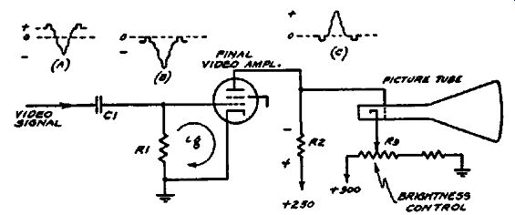
Fig. 10-17. A widely used type of d-c restorer circuit in which the video
amplifier output tube is operated at zero bias so that the grid-cathode elements
function as a di ode to reinsert the d-c component.
When the receiver is first turned on, there is no voltage drop across the plate-load resistor R2 until the output video tube warms up and draws plate current. The final adjustment of the brightness control therefore should not be attempted until the receiver has been turned on for a few minutes. In particular the brightness control should be all the way to the left (with the rotor at +300) until the receiver has warmed up; this is done to avoid possible damage to the picture tube because of excessive beam current.
The Contrast Control
The "contrast control" is the gain control which determines the magnitude of the video signal applied to the grid of the picture tube. Its counterpart in a sound receiver is the volume control, and in the same way that the sound volume control determines the range of intensities between the loudest sound and the softest sound, so the video contrast control determines the range of light intensities between the highlights and the shadows of the picture.
Referring to Fig. 10-16, the setting of the contrast control deter mines how much of the picture tube characteristic is used and how bright will be the brightest element of the scene. When the contrast control is not advanced far enough, the picture lacks brilliance and the highlights are comparatively dark; when the contrast control is advanced too far, the picture becomes blurred, there is a loss of detail in the highlights, and in general the inter mediate shades are lost.
Synchronizing Circuits
The circuits devoted to synchronization in a television receiver are those which remove the sync information contained in the complete video signal and utilize it to control the timing of the horizontal and vertical deflection oscillators. To perform these functions, the sync part of the signal must first be separated from the picture part of the signal. In addition the vertical sync pulses must be separated from the horizontal sync pulses so that each can be applied to the respective deflection oscillator which it controls.
The circuits used to separate the synchronizing pulses from the picture portion of the signal are called "sync separators" or "clippers." These circuits are designed so that they are responsive only to the sync pulses which lie above the pedestals; thus they reject the picture portion of the signal. The clipper or sync separator is generally followed by additional amplification and finally the sync signal is fed to a frequency-selecting circuit which separates the horizontal sync pulses from the vertical sync pulses.
This separation is accomplished by circuits which depend for their action upon the difference in the time duration of the two types of pulses.
To illustrate the principles involved in sync circuits, we shall describe the circuits used in the RCA Model TRK-12 receiver.
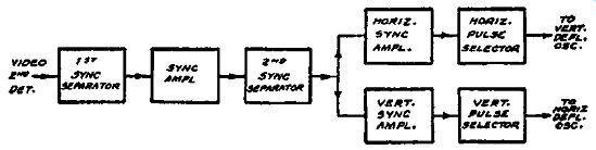
Fig. 10-18. Block diagram of the sync circuits used in the RCA Model TRK-12
receiver.
As the block diagram in Fig. 10-18 shows, the video signal is taken directly from the second detector and passes through the first sync separator which removes most of the video signal from the sync signal. The sync signal is then amplified in a sync amplifier stage and fed to a second sync amplifier stage which completes the separation of the sync signal. The output of the second clipper is fed to two separate stages, the horizontal sync amplifier and the vertical sync amplifier. The output of the horizontal sync amplifier feeds the sync pulses to a circuit-the horizontal pulse selector-which selects the vertical sync pulses; the output of the vertical sync amplifier also feeds the sync pulses to the vertical pulse selector which selects the vertical pulses.
On the whole, the block diagram presents quite an imposing array of circuits considering that it represents but a small part of all the circuits in the complete receiver. However, synchronization is so important in the operation of the television system that great care must be taken to make the synchronization positive in action.
Sync Separator Circuit
Referring to the partial schematic in Fig. 10-19, the video signal is fed from the second detector directly into the grid of the first sync separating tube. This stage uses one section of the 6N7 dual triode. The distinguishing features of this stage are that the tube is operated at the very low plate voltage of 15 volts and at zero bias (when no signal is present). When a signal is being received the grid leak-condenser combination R75-C77 provides a bias voltage as a result of the rectified grid current. As the waveform shows, the polarity of the video signal applied to FIG. 10-19. Schematic of the sync circuits used in the RCA Model TRK-12 receiver. Note the signal waveforms at the various points in the circuit.
the grid is negative so that the grid bias is supplied by the sync pulse part of the signal. As previously explained in connection with d-c restorer circuits, the bias at the grid varies in accordance with the average brightness and the result is that all the sync pulses are lined up with the zero-voltage axis at the grid of the first sync separator. This is illustrated in Fig. 10-20 which shows the plate current-grid voltage characteristic of the first sync separator stage.
Because of the low plate voltage of only 15 volts, plate-current cutoff is reached at a low value of negative grid voltage. Consequently the picture part of the signal lies beyond cutoff, and only the sync pulses are effective in causing the plate current to change. Thus the picture part of the signal is removed and so does not appear in the plate circuit of the first sync amplifier tube. An important part of the action in this circuit is the operation with grid leak bias so that all the sync pulses are lined up.
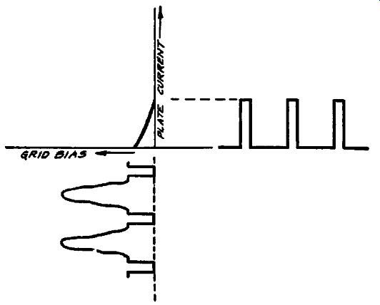
Fig. 10-20. The plate current grid bias characteristic of a sync separator
stage. The sharp cut-off enables the separation of the sync pulses from the
video signal.
As in the d-c restoring circuits, the time constant of the input circuit is sufficiently large so that the bias is maintained during the interval between sync pulses.
The signal produced in the plate circuit of the first sync separator no longer contains the picture part of the signal but instead the latter has been removed because of the sharp cutoff of this stage. A term often used to describe the action of a circuit similar to the first sync separator is the term "clipper." This term is appropriate because the stage can be thought of as clipping the video portion of the signal and leaving only the sync pulses.
The clipped sync signal is next fed to the grid of the second triode of the 6N7 which is arranged to function as an amplifier.
For this reason a high value of plate voltage, 200 volts, is used.
Note that the sync pulses have been reversed in polarity so that the grid of the amplifier tube goes negative on the peaks of the sync pulses. However, the operating characteristics of the amplifier stage are such that the sync pulse waveform in the plate circuit of the sync amplifier is simply an amplified version of the signal in the grid circuit. The polarity of the signal is of course reversed 180 degrees so that the sync signal in the grid circuit of the following clipper tube is negative in polarity.
The action in the second sync separator is similar to that in the first sync separator. A screen grid tube is used with the screen placed at a higher voltage than the plate and with both these voltages comparatively low. Thus the screen voltage is only 25 volts and the plate voltage about 6 volts. Under these conditions the stage has a very effective clipping action on both the positive and negative peaks of the sync pulse. In this way, if any video signal still remains it is clipped sharply by the plate-current cut off; at the same time, the positive peaks of the sync pulses are again clipped as in the previous sync separator. As a result of this second clipping of the sync pulses, the waveform is made flat and any noise components that may have been added to the signal are removed. Thus noise is prevented from interfering with the synchronization.
The output of the second sync separator feeds the sync pulses to two separate amplifier stages, a vertical sync amplifier and a horizontal sync amplifier. These individual stages provide further amplification of the sync pulses and at the same time act as buffer stages to isolate the vertical sync circuits from the horizontal sync circuits. The circuits used in the output of these stages are frequency-selecting circuits which differentiate between the two types of sync pulses by making use of the fact that the duration of the vertical sync pulses is greater than that of the horizontal sync pulses.
Horizontal Sync Selector
The signal is coupled to the horizontal sync amplifier through the 820-mmf condenser CB4 in Fig. 10-19. The amplified signal appears across R87 and is fed to the selector circuit consisting of C87 (150-mmf) and R90 (470 ohms). This circuit separates the horizontal sync pulses, which appear across R90. The manner in which this selector circuit operates requires some explanation. Essentially the current which passes through R90 is limited by C87 because of the small value of capacitance and the low value of resistance. As a result the current through R90 is proportional to the rate of change of the sync pulse voltage and in this way sharp voltage pulses are produced across R90. This is clearly illustrated in Fig. 10-21 which shows the input sync signal during the interval between successive fields. Note that at each edge of the sync signal where the waveform changes abruptly, this rapid change results in a pulse of current through C87 and R90, which produces the voltage drop across R90 shown in the figure. As explained later, only the positive pulses across R90 are effective in synchronizing the deflection circuit; those ...
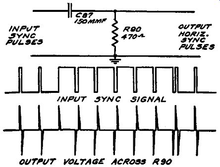
Fig. 10-21. Circuit used for separating the horizontal sync pulses from the
complete sync signal. The waveform of the sync signal at the input and output
of the separator are shown below the circuit.
... below the axis have no effect. As Fig. 10-21 shows, horizontal sync pulses are also produced during the vertical blanking period because the leading edge of each vertical sync pulse represents a rapid change of voltage and therefore produces a pulse through R90.
Vertical Sync Selector
The complete sync signal is also fed from the second sync separator into the grid of the vertical sync amplifier. The amplified sync signal appears across R99 of Fig. 10-19 and is fed to the selector circuit consisting of R101 and C98. Two additional sets of resistor-condenser combinations are used in series in order to increase the effectiveness of the vertical pulse selection.
The action of R101 and C98 in differentiating between the vertical and horizontal sync pulses is a direct result of the longer duration of the vertical pulses. Thus Fig. 10-22 shows that each one of the sync impulses, including the horizontal impulses, con tributes a small amount of charge which is stored in the con denser. The greater the duration of the pulse, the greater the voltage across the condenser. During the transmission of the long vertical sync pulses, the accumulation of charge on the con denser is greater than during the transmission of the short line sync pulses. As a result, the voltage across the condenser C98 ...
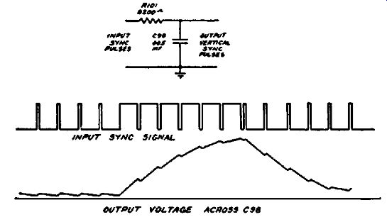
Fig. 10.22. Circuit used for obtaining the vertical sync pulses for field
synchronization. The input and output waveforms are shown below the circuit.
... builds up to a peak once during each field or 60 times in each second. As the figure shows, the vertical pulse builds up to a maximum at the end of the last vertical sync pulse and then steadies down to an average value of voltage which remains constant until the beginning of the next field pulse.
To increase the circuit effectiveness, two more similar resistor condenser combinations are used in series as shown in Fig. 10-19.
These circuits accomplish a further selection of the two pulses so that a sharper pulse is produced once during each field. The peak of this pulse is used to synchronize the vertical deflection oscillator.
For exact interlacing it is important that the vertical pulses produced at the output of the vertical selector circuit be the same on alternate fields. The equalizing pulses, previously described, accomplish this by making the conditions exactly the same before and after the transmission of the actual broad vertical sync pulses. As a result, the condenser charges up to the same value of peak voltage on both the odd and even fields so that the vertical oscillator is maintained in perfect timing.
Deflection Circuits
The block diagram of Fig. 10-23 shows the essential parts of a common type of deflection circuit for television. From the sync separator described in the previous section, horizontal sync pulses ...
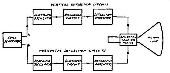
FIG. 10-23. Block
diagram of the essential parts of a widely-used type of deflection circuit.
... are applied to the horizontal deflection circuits and vertical sync pulses to the vertical deflection circuits. Both sets of deflection circuits contain the same type of elements, the principal difference being the operating frequencies.
The sawtooth waves required for deflection of the electron beam are formed in the discharge circuit. This circuit includes a con denser which is slowly charged from the B supply and then rapidly discharged through a vacuum tube. The voltage across this condenser varies in such a way as to form a sawtooth voltage wave. The exact moment at which the discharge tube operates is determined by the blocking oscillator which provides pulses to the grid of the discharge tube of sufficient amplitude to "trip" it. The frequency of the blocking action is itself synchronized with the incoming signal by pulses from the sync separator. The sawtooth voltage wave formed in the discharge circuit is amplified in the deflection amplifier and then applied to the deflecting yoke or plates which cause the scanning action of the beam in the picture tube.
Circuits for Electromagnetic Deflection
The schematic, Fig. 10-24, shows the deflection circuits used in the RCA Model TRK-12 and Westinghouse Model WRT-703 receivers. These are examples· representative of circuits for use with a picture tube deflected by the electromagnetic method.
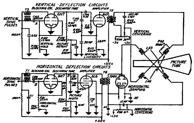
FIG. 10-24. Deflection circuits used in the RCA Model TRK-12 receiver. Compare
with the block diagram in Fig. 10-23.
To describe the formation of the sawtooth wave, let us assume that the grids of the 6N7 tube (in the horizontal circuit) are biased to cutoff so that the tube is non-conducting. The plate voltage starts to charge the .001-mf condenser 090 through resistors R93, R94 and R95 in series. The voltage across 090 (from D to ground) rises to form the trace part of the deflection voltage.
About 65 microseconds later, a positive pulse of voltage is applied to the grids of the 6N7 and the tube "trips" or starts conducting.
The triode section, whose plate is connected to D, then acts as a short to ground and discharges C90 in about 11 microseconds.
The voltage across C90 falls rapidly to form the retrace part of the deflection voltage. The discharge is stopped after 11 microseconds by a sudden blocking of the grids, and the charging cycle starts again. The relatively short time allowed for the charge and discharge of condensers C90 (horizontal) and C103 (vertical) assures that the sawtooth wave will be essentially linear.
Blocking Oscillator. The periodic blocking and tripping of the 6N7, which has just been mentioned, is accomplished by the blocking oscillator. In connection with the latter, the question naturally arises as to why the sync pulses could not be used directly to trip the discharge tube. Actually, the sync pulses could be used directly, but it has been found more satisfactory to use the blocking oscillator circuit being described. The blocking oscillator provides a steep pulse of high amplitude which is more readily adapted to the control of the discharge tube than is the sync pulse itself. The necessary timing of the blocking oscillator is of course obtained from the sync pulses.
As the name implies, the blocking oscillator is a regenerative oscillator in which the feedback is so large that the oscillator is blocked on the first cycle of oscillation. Thus when oscillation starts, the amplitude is so great that the negative charge which accumulates on the grid condenser drives the tube to cutoff. Be fore the oscillations can start up again, the charge on the grid con denser must leak off. The rate at which this charge leaks off determines the rate at which the steep pulses are produced by the blocking oscillator. Because the circuit constants are such that the natural frequency at which the oscillator attempts to work is higher than the frequency of blocking, the pulse produced when oscillations start has a very steep waveform which is advantageous in controlling the discharge tube.
The rate of blocking, and hence also the rate at which the pulses for the discharge tube are produced, is controlled by R91 and R92. The lower the value of this grid resistance, the more rapidly the charge leaks off so that the oscillations can begin again and produce another pulse. The "free-running" frequency of the blocking oscillator is thus controlled by the value of C89, which determines the amount of charge stored in the grid circuit, and R91 and R92 which determine the rate at which this charge leaks off.
In practice, the free-running frequency is adjusted by means of the horizontal hold control R92 so that it is lower than the line frequency of 13,230 cycles. The application of the horizontal sync pulse to the grid circuit, as shown, will then introduce a positive pulse into the grid circuit and cause the blocking oscillator to start operating slightly before the instant when it would normally resume operation. In this way the sync pulse keeps the blocking oscillator exactly in synchronism with the frequency of the scanning at the camera tube.
The circuit for the vertical deflection operates in the same manner. In this case R106, the vertical hold control, is adjusted so that the free-running frequency of the vertical oscillator is slightly less than 60 cycles. The introduction of the vertical sync pulse trips the oscillator just before it would otherwise resume oscillation so that the frequency is kept in synchronism with the vertical sync pulses.
Width and Height Controls. The peak value of the sawtooth voltage which is developed across C90 depends on the setting of R94. Since the peak value of the voltage across C90 determines the magnitude of the horizontal scan and therefore the picture width, R94 is called the picture width control. Similarly R108 controls the vertical sawtooth amplitude and therefore is called the picture height control.
The vertical linearity control R113, which is in series with the vertical wave-forming condenser C103, corrects the waveshape so that a sawtooth wave of current will be obtained through the deflecting coils.
Centering. As a result of the circuits described, accurately timed sawtooth voltages are available at points C and D of Fig. 10-24. These waves are amplified and coupled to the deflecting coils L44 and L43 by transformers T2 and T4 respectively. The picture is centered on the picture-tube screen by sending a small direct current through the deflecting coils. Potentiometers are provided for making the vertical and horizontal centering adjustments.
Damping Tube. The 5V 4G diode shunted across the secondary of T4 is provided so as to prevent transient voltages being set up when the scanning current changes abruptly. This diode acts as an automatic switch so that the transformer is loaded only during the trace period, and the load removed during the retrace period.
It is not possible to use a permanently-connected resistor load in place of the diode switch because this continuous loading would tend to prolong the retrace period by an excessive amount.
Electrostatic Deflection
In electrostatic deflection systems for television, it is usual to use the same type of sawtooth-wave generator as is used for electromagnetic deflection. The output systems, however, are quite different. To avoid distortion of the raster and defocusing of the spot, the sawtooth waves on each plate of any pair must be alike but 180 degrees out of phase. A balanced amplifier using a phase inverter is used to furnish these deflecting voltages. The force acting on the electron beam is thus due to the difference between the potentials of the two plates, since at any one instant the positive voltage on the one plate attracts the electron beam at the same time that the corresponding negative voltage on the other plate repels the electron beam. Thus, if at any instant the deflecting voltage on one plate is +50 volts, then the voltage on the other plate is -50 volts and the effective deflecting voltage is the sum or 100 volts.
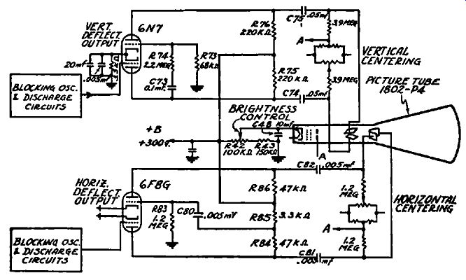
Fig. 10-25. Circuits used for electrostatic deflection in the RCA Model TRK-5
receiver. Note the push-pull output in both the horizontal and vertical channels.
Electrostatic Deflection Circuits. Fig. 10-25 shows the output circuits of the electrostatic deflection circuits used in the RCA TRK-5 and Westinghouse WRT-701 receivers. The blocking oscillator and discharge circuits are shown in block form because they are similar to those shown in Fig. 10-24. In the vertical circuit the signal across R75 is fed to one of the vertical deflecting plates through condenser C7 4. This same signal is also fed to the grid of the phase inverter section of the 6N7 tube through con denser C73 and a voltage divider consisting of R7 4 and R73. The signal across the phase inverter load R76, which is 180 degrees out of phase with the signal across R75, is fed through condenser C75 to the other vertical deflecting plate. The voltage divider R7 4, R73 is used to compensate for the gain of the phase inverter section of the 6N7 so that the signal amplitude applied to each deflecting plate is the same except for the phase reversal. In the case of the horizontal deflecting circuit, the action is similar; here the voltage divider consists of RB4 and R85.
Centering Control. Fig. 10-25 also shows the type of centering circuit used with electrostatic deflection. One plate of each pair is returned to the second anode through a high resistance. The second plate is returned through a high resistance to the potentiometer which permits a d-c voltage, either zero, plus or minus with respect to the first plate, to be applied to the second plate in order to center the raster on the screen of the picture tube. These potentiometers, called centering controls, are usually adjusted during installation and seldom need readjustment. The details of this type of circuit are shown in Fig. 10-26 in the following section on power supplies.
Power Supplies
As a general rule, two separate rectifiers are used to supply the d-c voltages for television receivers. A low-voltage supply provides approximately 300 volts for the tubes associated with the amplifier, deflection, and sync circuits of the receiver. A separate high-voltage power supply provides the high voltages-from approximately 2000 to 10,000 volts-required for the picture tube.
Since the low-voltage power supplies are very similar to those used in radio receivers, a separate low-voltage schematic is not shown here. The regulation in a television low-voltage power supply is generally better than that in a radio receiver because of the importance of preventing variations in the numerous circuits from interfering with each other and with the picture. The hum level is also kept down to a lower value because of the large number of circuits and stages, and because hum which would be inaudible in a sound receiver may cause appreciable distortion of the picture.
Unlike the low-voltage power supply, a half-wave rectifier is invariably used in the high-voltage supply. The advantages of the half-wave rectifier are that the transformer does not have to be as large and that the peak voltage is reduced to about one-half the value required for full-wave rectification. Ordinarily the half-wave rectifier is not used in radio receiver power supplies because its output is harder to filter and because it cannot supply as much current to the load as the full-wave rectifier. However, these characteristics are not disadvantages in television receivers because only a very small current is drawn and a resistor-con denser filter can be used.
High-Voltage Power Supply in RCA TRK-5, Westinghouse WRT-701
The high-voltage power supply used in the RCA Model TRK-5 and Westinghouse WRT-701 receivers is shown in Fig. 10-26. A type 879 high-voltage half-wave rectifier is used, the complete path of the rectified current being from the low-voltage end of the secondary, through the secondary winding, the 879 rectifier tube, the first filter resistor R91, the second filter resistor R92, and the bleeder resistors from R93 to R98, inclusive, and back to the low-voltage side of the secondary.
R91 acts as a filter resistor and also limits the voltage and current through the first filter condenser C86. Good filtering is se cured by using a high value of filter resistance; R92 is 470,000 ohms, and in combination with the two .05-mf condensers provides adequate filtering. Note that large values of filter resistance rather than large values of capacitance are used to obtain the required filtering. The advantage of this is the reduced cost and size of the condensers; in addition, the smaller the size of the filter condenser, the less is the danger of fatal shock if one accidentally comes in contact with a charged or partly-discharged condenser. Nevertheless, the high-voltage filter condensers should always be discharged before any measurements are made so as to guard against the possibility of an open bleeder circuit.
In the circuit being described the cathode of the picture tube is near ground potential while the second anode is 2000 volts positive with respect to the cathode. The focusing anode is returned to the focusing control which places approximately 500 volts on this electrode. Centering of the beam horizontally and vertically ...
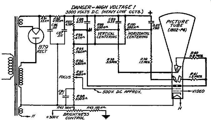
Fig. 10-26. High-voltage power supply used in the RCA Model TRK-5 receiver.
The heavy black lines represent the high-voltage circuits. Extreme caution
should be observed to avoid coming in contact with high-voltage points.
... is accomplished by returning one plate of each of the pairs through R40 and R41, to a common point which is at a voltage slightly lower than the maximum output of the power supply.
The remaining plates are then returned to the sliding taps on the horizontal and vertical centering potentiometers so that the voltages can be varied either positively or negatively with respect to the other plates. These circuits should not be tested while the power is on since the maximum high voltage is present on all the deflection plates and centering adjustments. The deflecting plates are capacitively coupled to the horizontal and vertical deflection out-put tubes through .05-mf and .005-mf condensers as shown in Fig. 10-25; these condensers are of course rated to withstand the full high-voltage output.
The high-voltage supply is not entirely independent of the low voltage power supply in the sense that the entire high-voltage power supply is returned to ground through the brightness control in the low-voltage power supply. If the connection to the bright ness control at R42, Fig. 10-26, were broken, then the entire high voltage power supply would "float." In actual operation, the potential at the cathode is approximately 200 volts above ground potential, depending upon the setting of the brightness control; as a result the low end of the high-voltage rectifier circuit, including the cathode of the picture tube, is above ground potential by this same amount. The control grid of the picture tube, which is tied to the plate of the 6V6 video output tube, is approximately 175 volts above ground potential so that the proper average brightness can be secured by means of the setting of R4f.
Grounding of High-Voltage Power Supply. The high voltage difference required between the cathode and second anode of the picture tube can be obtained with either the positive or negative side of the high-voltage power supply near ground potential. In receivers using the electromagnetic method of deflection, it is usual for the negative side of the power supply to be grounded since this enables coupling the video output tube to the modulation grid without the use of a high-voltage condenser. This same system is also used in some receivers which use electrostatic deflection, as for example in the RCA Model TRK-5 receiver. Where electrostatic deflection is used, however, high-voltage blocking condensers are required in the circuits which couple the deflection output tubes to the horizontal and vertical deflection plates.
To avoid the use of high-voltage blocking condensers in the deflection plate circuits and at the same time maintain the deflection plates at the same potential as the second anode (which is necessary to avoid distortion in the picture tube), the positive side of the high-voltage power supply is sometimes grounded and the cathode is then several thousand volts negative with respect to ground. The DuMont Models 180-183 are examples of receivers using this type of circuit. Although high-voltage condensers are not required in the deflection circuits, a high-voltage blocking condenser must be used between the plate of the video output tube and the modulation grid.
Regardless of whether the positive or negative side of the power supply is grounded, the usual precautions against electrical shock must be observed.
SIGNAL TRACING IN FACSIMILE RECEIVERS
Facsimile is similar to television in that both are concerned with the reproduction of pictures at a distance from the source. However, in facsimile the time required for the transmission of a single picture is ordinarily reckoned in terms of minutes whereas in television we have seen that a complete picture or "frame" must be transmitted in approximately one-thirtieth of a second.
In facsimile, a permanent record of the picture is made at the receiving point, whereas in television a transient or temporary image is obtained and no record is ordinarily available after the transmission has taken place. Unlike television, which presents a rapid succession of moving pictures to create the illusion of motion, facsimile deals with the reproduction of but a single picture which is permanently recorded by the facsimile receiver. This picture, which may be a reproduction of printed matter, a photograph, drawing, or any combination of these, can be examined after the several minutes required for its transmission have passed, and is available as a permanent record.
Because of the much greater period of time available for the transmission of a facsimile reproduction, it is to be expected that facsimile will use mechanical devices to a much greater extent than television. Present facsimile receivers and transmitters use mechanical scanning devices and synchronizing systems, rather than electronic systems as in television, although electrical impulses are of course used to control the mechanical motions. Thus to a considerable extent, the proper operation of a facsimile system requires that the system be in proper mechanical adjustment as well as in proper electrical adjustment.
At the present time a number of stations in the broadcast band regularly transmit facsimile programs which can be received with a conventional radio receiver in conjunction with a facsimile recorder. Since these stations transmit standard programs during the regular hours, facsimile broadcasts are limited to the early morning hours, generally between one a.m. and six a.m. There are also several stations operating in the ultra-high frequency range which provide facsimile programs during the day. In all cases standard broadcast or short-wave receivers which tune to these frequencies can be used to receive facsimile programs, since the bandwidth of the average receiver is entirely adequate.
The application of signal tracing to the servicing of facsimile receivers involves a knowledge of the overall operation of the system with special emphasis on the recorder. For this reason we shall devote the following paragraphs to a brief explanation of the Finch facsimile system which is quite typical of facsimile systems. Although other systems have been and are being used, these systems have much in common and the discussion of the Finch system will be of value in understanding other systems as well.
FIG. 10-27. A facsimile transmission system showing the major components used
in the transmitter and the receiver.
Finch Facsimile Receiver
In one form of the Finch system, the transmitter employs a scanning system which is illustrated in Fig. 10-27. The copy is fed through the scanning mechanism at the rate of 1/100 inch per second and at the same time it is scanned from left to right by a small beam of light about 1/100 inch in diameter. The amount of light which is reflected into the photocell is proportional to the shading of that element of the copy being scanned; a relatively greater amount of light is reflected into the photocell from elements where the copy is white than from darker elements. In this way the output of the photocell produces a pulsating voltage, the amplitude of which is proportional at every instant to the brightness of the elements being scanned.
The output of the photocell is amplified and is used to control the amplitude of a 2000-cycle signal voltage. This 2000-cycle signal is essentially a carrier which is modulated by the output of the photocell so that its amplitude varies in accordance with the amount of light reflected from the copy. Finally the modulated 2000-cycle signal is fed to the transmitter where it modulates the radio-frequency carrier. Because of the relatively low scanning speeds, as compared with television, this r-f carrier may lie in or below the broadcast band; the bandwidth necessary is even smaller than that required for ordinary sound broadcasting.
As the diagram shows, the transmitted signal is received by a conventional receiver which is connected to the facsimile recorder.
After rectification, the 2000-cycle modulated signal is fed to the recording stylus where it traces out the image on the specially treated copy paper. This paper is a white-coated carbon-impregnated paper designed so that it turns various shades of gray or black in proportion to the current which passes from the stylus through the paper.
The required horizontal deflection of the stylus as well as the vertical movement of the copy paper is secured by means of a motor-driven arrangement which is essentially similar to that used at the transmitter. In order to obtain synchronization, the stylus is driven through a friction clutch which makes it possible to hold the stylus at the beginning of each line for whatever small time interval is required to synchronize the stylus with the photocell scanning at the transmitter. The exact moment at which the stylus is released is determined by a 500-cycle synchronizing signal which is transmitted at the beginning of each line. It is for this reason that the carrier generator in the dia gram is designated as a two-tone generator since it produces a 2000-cycle tone during the active line scanning, which is changed automatically at the transmitter to a 500-cycle tone at the beginning of each line. In practice the stylus at the recorder is driven about 2% faster than the photocell at the transmitter so that it will be possible to synchronize the scanning. A little reflection will make it clear that this is required since otherwise the stylus in some cases might not have reached the extreme left position at the instant of arrival of the sync signal.
A more detailed description of the recorder can be obtained with the aid of the diagram in Fig. 10-28 which is a schematic of the Finch Type RB home facsimile recorder. The signal voltage is obtained from the output of the audio amplifier of the receiver used in conjunction with the recorder and is fed to the rectifier circuit. The rectifier employs a full-wave circuit in which a 6A6 is used with the grids and plates tied together.
Fig. 10-28. Schematic diagram of the Finch facsimile recorder.
Circuit Analysis
To analyze the circuit, let us first consider the circuit connections when the recording arm, which carries the stylus, has just returned to the extreme left of the paper. This is the condition shown in Fig. 10-28. For this case, the projection on the clutch disc holds the stylus in the left position to await the transmission of the 500-cycle sync signal which will release the disc by attracting the clutch control armature. While the stylus is at the left side of the paper, the signal transfer control cam automatically throws the signal transfer switch to the down position so that the following circuits are affected: (a) The stylus is disconnected from the circuit so that no voltage will be fed to the stylus.
The shape of the control cam is such that the stylus is also disconnected on the return movement of the stylus to the left side of the paper so that no impression is made on the copy paper during the return trace. (h) The sync signal selecting condenser is shunted across the secondary winding of the rectifier input trans former in order to bypass the 2000-cycle facsimile signal, and thus prevent it from energizing the electromagnet and prematurely releasing the clutch disc before the 500-cycle sync signal is transmitted. ( c) The electromagnet winding is connected to the cathode of the rectifier tube so that the rectified 500-cycle sync current will cause the electromagnet to attract the clutch control armature, so as to start the stylus across the copy paper at the proper instant.
At the same time that the clutch control armature permits the clutch to engage, and the stylus starts across the paper, the switch control cam throws the switch to the "up" position, and the following actions take place: (a) The stylus is connected to the cathode of the 6A6 rectifier tube so that the signal voltage is impressed on the stylus, (b) The electromagnet is disconnected from the cathode of the rectifier tube so that no current will flow through the winding, ( c) the sync signal selector condenser is disconnected from the secondary winding of the transformer so that it will not bypass the 2000-cycle marking signal.
Servicing the Receiver
From the foregoing description of this typical facsimile system it can be seen that the servicing problems in facsimile will be largely mechanical rather than electrical. So far as the mechanical problems are concerned, these are fully described in the service notes and can hardly be said to fall within the scope of signal tracing. However, insofar as the electrical part of the system is concerned, signal tracing is of definite value in localizing the trouble in facsimile systems.
For our present purposes, we can divide the complete facsimile receiver into two parts: the radio receiver which includes the audio amplifier, and the recorder which includes the signal rectifier unit and the sync circuits. The servicing of the radio receiver part of the facsimile receiver requires no further discussion here since it is a conventional radio receiver. If the receiver works properly on ordinary broadcast signals, then its operation will be satisfactory for the reception of facsimile signals. However, for proper operation of the recorder, the output of the receiver must be sufficiently high and the output must be properly matched to the recorder input transformer in order to avoid loss of signal amplitude.
To check the operation of the signal rectifier unit, a 2000-cycle signal can be fed to the input transformer and its progress checked through the secondary winding, through the transfer switch, and finally to the stylus. Before this test is made the motor shaft should be rotated by hand so that the stylus is in the middle of the line and the signal transfer switch in the "up" position so as to feed the signal to the stylus. Similarly, to check the operation of the sync circuits, the shaft should be rotated so that the stylus is at the extreme left of the line and a 500-cycle signal should be applied to the input transformer. Using standard practice, this signal can be traced to the secondary winding and should produce a rectified voltage across the electromagnet relay windings of sufficient magnitude to attract the armature. The operation of the recorder can also be checked while a transmitted facsimile signal is being received.
In every case, the manufacturer's service instructions should be referred to before attempting to service facsimile recorders. In general such notes contain the procedure for making the necessary mechanical adjustments as well as hints on characteristic troubles which develop in particular recorders. As a general rule, these data also contain information on the normal voltages required, including the average values of signal voltage required at the stylus, and across the electromagnet windings. This information is of course very helpful in localizing defective conditions.
FREQUENCY MODULATION
Up to the present time all broadcast stations have used amplitude modulation for program transmission. In this method of transmitter operation the frequency of the carrier is maintained constant, usually by crystal control, while the amplitude of the carrier is varied by the audio modulation impressed upon it. A new system of broadcast transmission by frequency modulation is now being introduced by a few stations in the East. This system was devised by Major E. H. Armstrong and differs from amplitude modulation in that the carrier frequency is varied by the impressed audio modulation, while the carrier amplitude is held constant.
Advantages of Frequency Modulation
The principal advantages of frequency modulation over amplitude modulation are an improved signal-to-noise ratio, particularly in poor reception areas where the signal strength of the transmitter is weak, and a reduction in interference when two frequency modulated transmitters are geographically separated but operating on the same frequency. In receiving, better fidelity is usually more easily obtained from frequency-modulated transmissions.
Since the carrier frequency in frequency-modulated broadcasting is varied over a wide band, wide channels are necessary for transmission. Present channels are 200-khz wide and have been allocated in ultra-high frequency bands to avoid interference with other services which would result if channels of such width were assigned within the standard broadcast band. The actual carrier frequency variation is limited to one-half the channel width, as with amplitude modulation, since the frequency of the carrier varies above and below the nominal assigned value when audio modulation is applied. In present frequency-modulated broadcast transmissions, the maximum frequency deviation is held to approximately plus or minus 75 khz during audio modulation.
How Noise is Reduced
The manner in which frequency modulation reduces noise may be understood by remembering that most electrical noises change the amplitude of the signal but not its frequency. Now, in the amplitude modulation method of broadcasting, both noise and audio modulation act to vary the carrier signal voltage so that the two are combined in the signal detected by the receiver. In frequency modulation, however, the audio modulation varies only the frequency of the carrier signal and not its amplitude.
Noise, on the other hand, will cause no change in the carrier frequency, though it will affect its amplitude. If, then, the receiver is designed to detect only variations in signal frequency and not variations in amplitude, noise resulting from amplitude modulation is eliminated. Frequency modulation is not perfect, but a very great reduction in noise is secured by this method.
Special Receivers Necessary
Conventional broadcast receivers are designed only for the reception of amplitude-modulated transmissions and therefore are not suitable for receiving frequency-modulated broadcast signals. The principal differences in the latter are in the design of the detector and in the limiter stage which precedes the detector.
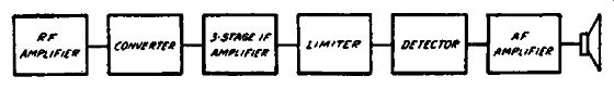
Fig. 10-29. Block diagram of a receiver for the reception of frequency-modulated
signals. With the exception of the limiter stage, the lineup is similar to
that of a conventional superheterodyne receiver.
A typical stage-by-stage lineup for a frequency modulation receiver is shown in Fig. 10-29. This shows an r-f amplifier, converter, 3-stage i-f amplifier, limiter, detector and a-f amplifier.
Since the transmitted frequency varies about 75 khz above and below the point to which the receiver is tuned and flat amplification is necessary for high-quality reproduction, the carrier-amplifying stages and the converter must be designed to pass a 150 -khz band without frequency discrimination. Ordinary tuned circuits are usually far too sharp for this purpose, particularly in i-f circuits, so we find in the frequency modulation receiver that low-Q circuits are necessarily employed to achieve broad tuning.
In the i-f stages, broad-band reception is secured by using a high intermediate frequency, usually of the order of 3 mega cycles, and by broadening the i-f transformer response by resistance shunted across one or more windings.
What the Limiter Does
The limiter stage requires detailed consideration. Its purpose is to smooth out any variations in carrier amplitude so that it may pass on to the detector circuit a signal which is constant in voltage but varies in frequency. This is done by designing the circuit and operating the tube so that it overloads even when a weak signal is being received. Then any increase in signal voltage will not cause an increase in the carrier signal voltage which appears across the tuned circuit forming the limiter stage plate load. The high gain in the r-f, converter and i-f stages provides sufficient amplification even for weak signals so that the actual signal voltage at the limiter grid during reception will always be several volts. Any applied signal voltage greater than the over load point causes rectification in the grid circuit. A resistor in series with the grid return of the limiter input circuit is installed so that the grid current resulting from rectification in this circuit causes a voltage drop across the resistor which can be utilized to provide avc action. This avc voltage is applied, through appropriate filters, to preceding i-f, converter and r-f stages.
Special Detector Used
Since, in frequency modulation, the a-f modulation causes a variation in carrier frequency, we need a type of detector which will convert these frequency variations into the a-f signal voltages which originally produced these carrier frequency variations, and in this way restore the original modulation. Ordinary detector circuits are not suitable, since they give an output voltage which is proportional to the amplitude of the carrier modulation and not to the carrier frequency. Since the voltage output of the discriminator circuits employed in afc designs varies with the frequency shift of the applied carrier signal, it serves as an ideal device for the detection of frequency-modulated signals.
A typical afc discriminator circuit is shown in Fig. 10-30. The primary coil, L1, of the discriminator transformer is connected in the plate circuit of the limiter tube and is closely coupled to the center-tapped secondary L2, L3. When the transformer secondary circuit is tuned to resonance with the alignment frequency of the i-f system, the voltages E2 and E3 are equal but opposite in phase. Since the d-c voltage across the discriminator load resistors, R1 and R2, occurs as the result of rectification of E2 + E1 and E3+ E1, then, at resonance, the d-c voltage from point B to ground is equal to that from point B to A, as both R1 and R2 are similar resistors. However, because of the manner in which the diodes are connected, the resulting d-c voltages will be opposite in polarity. Therefore, the voltage across Rt …
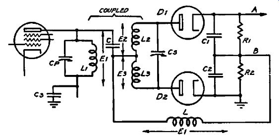
Fig. 10-30. The second detector of a receiver for frequency-modulated signals
is similar to the discriminator circuit shown above.
… will cancel that across R2 and a measurement from point A to ground will show zero voltage between these two points when the circuit is tuned to resonance with the alignment frequency. This is the normal condition for perfect alignment of an afc circuit.
When the signal voltage applied to the discriminator trans former is higher or lower in frequency than that to which it is tuned, the voltages E2 and E3 will remain equal but their phase relationship with respect to Et will change. As a result, E2 + E1 will no longer equal E3 + E1. Since this becomes the case, the resulting d-c voltages across R1 and R2 will no longer be equal and opposite in polarity and a voltage with respect to ground will accordingly appear at point A. As the frequency of the carrier signal becomes higher or lower than that to which the discriminator is tuned, the voltages developed across R1 and R2 add or subtract. Since point A is at zero voltage at resonance, this signal frequency variation causes point A to assume a potential with respect to ground which varies in a positive or negative direction in accordance with these frequency variations. The change in voltage of point A with respect to ground as a result of this shifting frequency is represented in the diagram, Fig. 10-31.
How the Discriminator Detects
Now let us see how this characteristic of the afc circuit serves to supply an audio signal to actuate the a-f amplifier of the receiver. We have seen, in frequency-modulated transmissions, that the carrier frequency changes at a rate which is in accordance with the audio modulation impressed upon the carrier. Let …
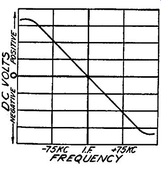
Fig. 10-31. The output voltage of the second detector varies in accordance
with the amount by which the signal frequency differs from the intermediate
frequency.
… us assume that a 400-cycle audio note is being broadcast and the nominal frequency of the transmitter is 42 mhz. On the positive half of the 400-cycle modulation, the carrier frequency may be increased while on the negative half it may decrease. If the modulating voltage is sufficient, this may cause a maximum increase of carrier frequency of 75 khz so that the maximum frequency at the peak of the positive half of the wave becomes 42 mhz + 75 khz and, at the peak of the negative half of the cycle, to 42 mhz - 75 khz. Now, referring again to Fig. 10-31, we see that a carrier frequency shift in a negative direction will cause the output voltage of the discriminator to become positive whereas an increase in carrier frequency will cause this output voltage to become negative. Since a 400-cycle note is being broadcast, the carrier frequency increases and decreases and the output voltage of the discriminator becomes positive and negative at the same rate, 400 cycles per second, as that of the original broadcast note. Now, if we apply this rapidly-varying voltage to the grid of an amplifying tube, the voltage across its output load will vary at the same rate. Since this is precisely what occurs when an a-c signal is applied to a grid, we see that in this manner detection of frequency-modulated signals is effected.
Once the frequency-modulated signal is converted into audio frequencies, any type of conventional audio amplifier is suitable.
Since the fidelity of reproduction in a carefully-designed receiver is exceptional, high-grade a-f amplifiers and speakers are usually employed.
The G-E Model GM125 Receiver
The schematic Fig. 10-32 shows the circuit of the G-E model GM125 receiver, which is designed for frequency-modulation reception. This is a 12-tube, single-band receiver which covers a frequency range of from 37 to 44 megacycles. A single r-f stage feeds the 6K8 converter; four i-f stages are employed, the fourth stage acting as the "limiter." The detector is similar to the afc discriminator previously described. The triode section of a 6Q7G is employed as the first a-f amplifier and feeds a 6J5G phase inverter which drives the push-pull 6L6G output tubes.
The r-f and converter stages are similar to those which could be employed in conventional designs for the same frequency band, except that no effort has been made to acquire selectivity in the tuned stages since this would be undesirable in a receiver which is required to pass a wide frequency band without frequency discrimination.
The i-f stages are designed to give a band width of 300 khz.
This is done by using a high intermediate frequency (3000 khz) and by shunting each i-f transformer primary winding with a 15,000-ohm resistor.
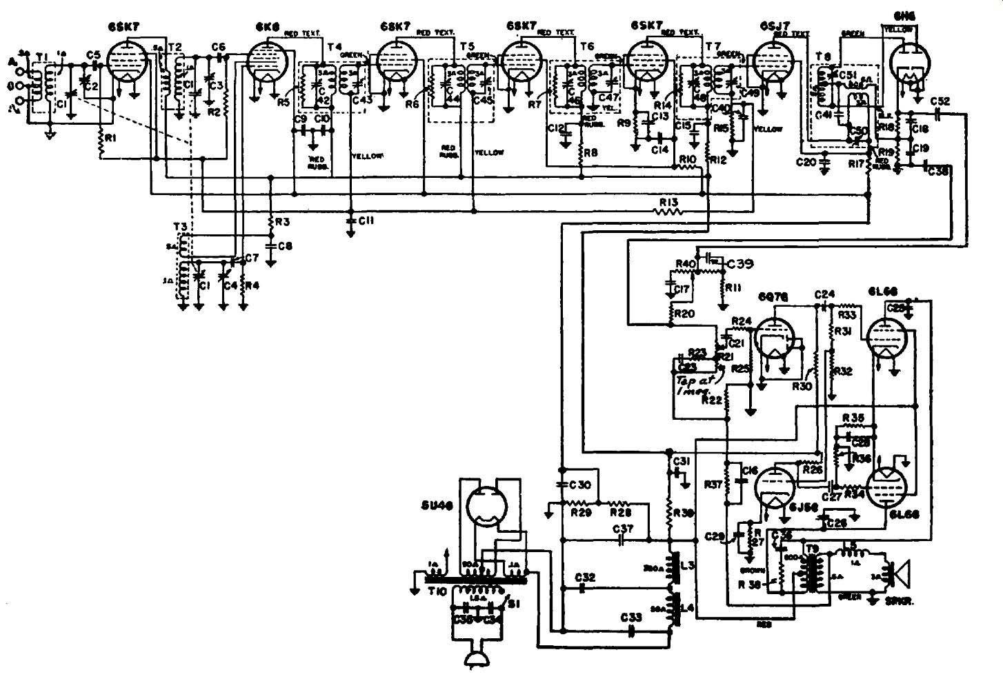
Fig. 10-32. Schematic of the G-E Model GM-125 receiver designed for the reception
of frequency-modulated signals.
The last i-f stage operates as a limiter. The limiting effect is secured by using a 6SJ7 tube in this stage and operating it with zero control grid bias and only 65 volts on the plate and screen.
Under these operating conditions, the tube overloads with a relatively small applied signal. The high overall gain of the stages preceding the limiter tube provides sufficient amplification so that even a weak signal in the antenna circuit is built up to a voltage sufficient to overload the limiter.
When the signal strength is sufficient to overload the limiter stage, grid current flows through the 330,000-ohm resistor, R15, in the grid return circuit of the 6SJ7. The resulting voltage drop across R15 is used to provide avc action and thus prevent over loading of preceding stages. By incorporating avc in this stage, there can be no avc action until the limiter is overloaded, which is its required operating condition. When such is the case, an increase in signal voltage applied to the limiter grid will cause no increase in the output signal voltage across its plate load but the grid current will increase, thereby assuring an increasing avc voltage.
The discriminator-type detector is similar in action to that reproduced in Fig. 10-30. It converts the frequency variations of the i-f signal output to a voltage which varies in amplitude at the audio frequency rate. The essential difference between this type of discriminator and one used solely for afc purposes is that the audio component is not filtered out. This must be done when such circuits are used for afc applications to avoid modulating the oscillator at the audio frequency. The discriminator load by-pass condensers, C18, C19, are accordingly only 22 u-u-f each in this circuit, so there is no by-passing of the higher audio frequencies.
The output of the frequency-demodulator is coupled to a tone control network composed of R11, R20, R40 and the shunt and series condensers C39 and C 17. Operation of R40 provides attenuation of either high or low frequencies, as desired. The output of this network connects to the volume control, R21, which returns to ground through an inverse-feedback network composed of R37 shunted by C16 in series with R22. The balance of the audio system is conventional.
Alignment Procedure
To align the i-f amplifier, connect an electronic voltmeter (or any other d-c voltmeter which has a high input resistance) across R15. Feed a 3 -mhz signal to the grid of the third i-f tube. Temporarily shunt the secondary winding of T7 with a 10,000 or 15,000-ohm resistor and adjust C48 until the voltmeter reading is a maximum. Then remove the secondary shunting resistor and adjust C49 for maximum reading on the voltmeter. Then connect the shunting resistor across T6 secondary, feed the 3 -mhz signal to the second i-f grid and peak the trimmers of T6 in the same manner. Repeat this process for each of the i-f transformers in turn until all are aligned.
The frequency demodulator circuit may also be aligned with the voltmeter and signal generator. Feed a 3 -mhz signal to the input of the i-f amplifier and connect the voltmeter from the cathode connection of R18 to ground. A small voltage reading usually will be indicated if the circuit is slightly out of adjustment. If not, adjust C51 until a reading is secured. Then adjust C50 until the voltage reading is a maximum. After this is done, adjust C51 until the voltmeter reads zero. The discriminator alignment is then complete.
The r-f and oscillator stages are aligned by feeding a 42.8 mhz signal to the antenna terminals and, with the receiver tuned to this point on the dial scale, adjusting the oscillator trimmer C4 for maximum reading on the voltmeter, which should be connected across R15. Then peak the antenna and r-f trimmers (C2 and C3) in the same manner.
The receiver may also be aligned with a special frequency modulated signal generator.