AMAZON multi-meters discounts AMAZON oscilloscope discounts
In order to truly grasp the operation of an automobile, one must eventually take one apart and put it back together again. Likewise, to attain a genuine insight into the workings of semiconductor devices you must take them apart and put them back together again using the "tools" of basic solid-state physics. We will disassemble the semiconductor down to its fundamental molecular structure so that you can observe and understand its action.
Electric current is present whenever electrons or other current carriers ( it will be pointed out that there is another kind) move.
Current carriers can be moved by applying a pressure (voltage). Transistors, diodes, and other semiconductors are nothing more than small "chunks" of solid material in which electric current can be controlled. This ability to control current is what makes the devices so very useful. In vacuum tubes, the current is through a vacuum, while in semiconductors, the current is through a solid. Thus semi conductors are often referred to as "solid-state" devices, and the key to understanding their operation lies in basic solid-state physics.
One of the basic problems is to become familiar with new terminology. However, new words and new ideas can add to the excitement of discovery if each one is fully understood before going on to the next.
When you complete this section, terms like majority carriers, reverse bias, junction, N-type or P-type semiconductor, and doping will all be familiar to you. A summation composed of a series of short and simple statements completes this section. Once these fundamentals are firmly established, the peculiarities of different devices can be easily understood.
CONDUCTORS, SEMICONDUCTORS, AND INSULATORS
The first step is to define a semiconductor. A good start would be to say that a semiconductor is a material whose characteristics lie somewhere between those of a conductor and of an insulator. This puts us in the right "ballpark," but it is not sufficient for a definition. By our being more specific about conductors and insulators the definition becomes clearer. The difference between a conductor and an insulator is in the atomic structure. A conducting material has a large number of electrons ( current carriers) ready to participate as current when the slightest pressure (voltage) is applied. The reason that copper is such a good conducting medium is that there are numbers of free electrons ready and willing to act as current carriers. This is another way of saying that the resistance (to current) of copper is low. Later you will see that this is because the electrons are loosely bound to the nucleus of the copper atom.
A good insulator, on the other hand, is a material in which the electrons are held very tightly by the nucleus. They are so tightly held that a voltage is required to tear them away from the nucleus to make current carriers available for conduction. The resistance of an insulator is very high. When enough voltage is applied to an insulator to cause it to conduct ( that is, when electrons are literally ripped away from the nucleus), the reaction is often so violent that the material is scorched or even destroyed.
Now if we agree that the characteristics of a semiconductor lie some where between those of a conductor and those of an insulator, you would then probably guess that the electrons are held firmly by the nucleus in a semiconductor-not too strong, not too loose. In other words, electrons don't immediately fall into conduction at the application of the slightest voltage as in a conductor; nor do they hold on so tenaciously to the point that you have to ruin the material in order to cause conduction, as is the case in the insulator.
A conducting material has many electrons available for current conduction. An insulator has no or few current carriers available for conduction. In a semiconductor material the number of electrons, or current carriers, available for conduction is few, but it can be easily increased by the application of a nominal voltage. Current carriers in a semiconductor material have not yet fallen into the flow, but by the application of a little pressure (voltage) they can be made to do so.
In a conductor there are many electrons that are immediately available.
In an insulator the current carriers are so tightly bound to the nucleus of the atom that they are not available for conduction.
The previous paragraph is very important and holds the key to understanding semiconductor theory. The electrical resistance of a device is determined by the number of current carriers. In a semi conductor device the resistance can be changed at will by merely varying the number of available current carriers. A semiconductor device is an easily controlled variable resistance.
With this basic idea in mind, take a closer look at how the number of current carriers available for conduction and thus the resistance of a semiconductor can be varied. Since this subject is probably quite new to you, it is necessary to go back to ground zero, make some basic definitions, and become familiar with the simple atomic structure of…
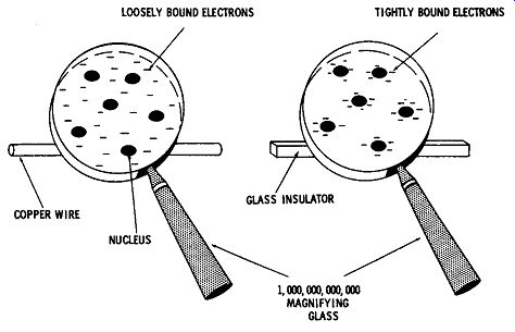
Fig. 1. A magnified conductor and insulator.
…a semiconductor crystal. We will do this by first noting how a semi conductor differs from a conductor and an insulator.
Good electrical conductors are copper, silver, gold, and aluminum.
The atoms of these elements have a large number of electrons that are loosely bound to the nucleus and easily become a part of the electric current. This situation is pictorially represented by Fig. 1A. Each black circle represents the nucleus of a copper atom, and each dash represents an electron tied to the nucleus. A magnification of 1,000,000,000,000 would be necessary to actually see this. It is easy for current to move in a conductor because the electrons or current carriers are readily available and loosely bound to the nucleus.
In some materials they are more loosely bound than in others.
Thus some materials are better conductors than others.
Fig. 1B shows a pictorial representation of an insulator such as glass, in which the electrons are tightly bound to the nucleus and a large voltage must be applied in order to produce electrical conduction.
This voltage usually is so large that when the electrons are finally ripped away, the material is physically damaged.
GERMANIUM AND SILICON
There are two common semiconductor materials-germanium and silicon. These materials are crystalline, as found in natural form. This is just another way of saying that when either germanium or silicon atoms unite to form a block of material, they do so by joining hands, so to speak, and share electrons to form a simple, symmetrical crystal.
The makeup of the germanium or silicon crystal is not nearly as complicated as the structure of a snowflake. As a matter of fact, the crystal line form of germanium or silicon is one of the simplest crystals. The formation is termed a crystal lattice.
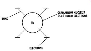
Fig. 2. Germanium atom.
First, look at a germanium atom as shown in Fig. 2. This atom has four electrons in the outer orbit that are loosely bound to the nucleus. For convenience' sake, the nucleus and the electrons that are tightly bound to it are contained in the circle marked Ge. A silicon atom could be represented in exactly the same way, except the Ge would be replaced with S1.
A number of these atoms combined form a crystal lattice, as shown in Fig. 3. Each atom contributes four electrons to the crystal structure and also shares those from the four adjacent atoms. Notice how this sharing results in a neat crystal structure. A silicon semiconductor material would look exactly like this except that the nucleus would be silicon rather than germanium.
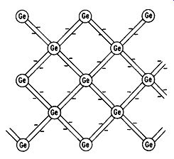
Fig. 3. A crystal lattice.
It is possible to produce conduction in this semiconductor material by applying a voltage that causes electrons to break away from the atoms and enter into conduction. This effect does not require high voltage as in the case of an insulator, but neither does the material act like a good conductor. It would be somewhere between an insulator and a conductor-a semiconductor. However, remember that the desired result is to be able to control the amount of conduction, and continue to investigate the properties of the crystal.
N-TYPE SEMICONDUCTOR
One of the principles that gives real importance to semiconductors is to introduce impurity atoms into the crystal lattice to obtain additional current carriers. This process of introducing impurity atoms into the basic crystal is called doping.
There are a number of doping materials, such as arsenic, phosphorus, and bismuth, that can be mixed with germanium. The atoms join into the crystal structure as though they were germanium. In other words, the germanium atoms have a "stranger" in their midst. The only difference is that the stranger has five electrons to contribute to the crystal, whereas germanium has only four. Since only four electrons are required to complete the crystal lattice there is one electron that is not bound to the crystal structure. The material having five electrons is called an impurity. In this case, the impurity atom has donated an electron to the crystal structure and is therefore called a donor atom (Fig. 4). Semiconductor materials that contain donor impurities are called N-type semiconductors. You can remember this by the fact that donor has an N in it or that the electrons that were contributed have a negative (N) polarity. The number of extra electrons or current carriers controls the resistance of a semiconductor material. Obviously, the more heavily doped materials contain more donor atoms, more extra electrons for conduction, and therefore have a lower electrical resistance.
DONOR IMPURITY (ARSENIC) ...
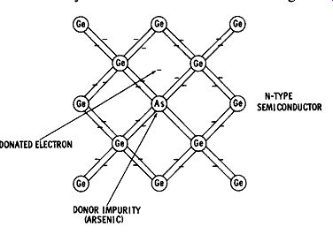
Fig. 4. Donor impurity. N-TYPE SEMI CONDUCTOR; P-TYPE SEMICONDUCTOR
You're way ahead if you're wondering about the possibility of atoms having three electrons that can be added to the semiconductor crystal.
Atoms with such properties are indium, gallium, and tellurium. Indium joins with germanium as shown in Fig. 5. Note that insertion of an impurity atom containing only three electrons leaves a hole in the crystal structure at a point where an electron is normally located.

Fig. 5. Acceptor impurity.
That is exactly what this lack of electron is called, a hole. An impurity atom that has only three electrons to contribute to the crystal structure is called an acceptor impurity because it is ready to accept an electron.
The semiconductor material that is produced is called a P-type semi conductor. You can remember this fact by using acceptor, or remember that the impurity produces positive (P) holes.
In other words, N-type semiconductor material has extra electrons donated by the impurity atom, while P-type semiconductor material has excess holes contributed by acceptor impurities. The number of excess holes or electrons determines the electrical resistance of the material.
Conduction in Semiconductors
Electrons can be made to move through a crystal of N-type semi conductor by applying a voltage that will exert a force on the electron.
Fig. 6 shows that electrons move through the crystal from the negative terminal to the positive terminal of the voltage source.

Fig. 6. Direction of electron flow.
Holes can also travel through a P-type semiconductor crystal (Fig. 7). When an electron in a crystal bond has enough force exerted on it to break the bond, it will jump into a hole. The hole has, in effect, moved from where it was originally to the place where the electron jumped out of the bond. Therefore it is easy to see that holes and electrons travel in opposite electrical directions through their respective materials. By applying a voltage to N-type material, we have electron flow, and by applying voltage to P-type material, we have hole flow.
At least it can be thought of as hole flow. You may be saying to yourself that it is actually electron movement, but it will be easier to understand semiconductor theory if you accept the proposition that the current carriers in N-type material are electrons and the current carriers in P-type material are holes.

Fig. 7. Direction of hole flow.
At this point we should review the fact that this entire situation can be duplicated by using silicon or possibly other materials as basic semiconductor elements. Also, it is impossible to have a perfectly pure N- or P-type semiconductor. An N- or P-type semiconductor contains donor or acceptor impurities purposely placed there. We must make a distinction between majority carriers and minority carriers. The majority current carriers are the electrons or holes that are free to move in the crystal structure, and the minority current carriers are the electrons or holes that are bound by the crystal structure and contribute to electric flow only under certain conditions.
In N-type material, electrons are the majority carriers and holes are the minority carriers. In P-type material, holes are the majority carriers and electrons are the minority carriers.
Let's recap our position by reviewing the material up to this point.
Pure semiconductor materials are doped with impurities to provide a given number of current carriers. The doping produces two kinds of crystals (N and P) and two kinds of current carriers (electrons and holes). Electrons are the majority carriers in N-type semiconductors, and holes are the majority carriers for the P-type semiconductors.
N-TYPE CRYSTAL P-TYPE CRYSTAL

Fig. 8. P- and N-type material.
Now that we understand how the semiconductor crystal is constructed and how the impurities provide electrons and holes as current carriers, let us change Figs. 4 and 5 and thus simplify the representation of a semiconductor crystal. Since the impurity atom con tributes an extra electron to the crystal, we show this in conjunction with a positive charge to make up the rest of the structure. Together, these two are electrically neutral. If, in the case of a donor impurity, the extra electron were removed from the atom, that remaining would have a positive charge. In the P-type material the impurity atom has a hole associated with it that has a positive charge, and therefore the rest of the atom can be considered negative. The entire impurity atom has a charge of zero--the positive hole balancing out the negative atom. Fig. 8 shows a representation of the P- and N-type materials.
The N-type. material has a number of free donor electrons associated with this large crystal structure ( the two taken together are neutral). The P-type material has a number of excess holes, each associated with an acceptor impurity atom.
JUNCTIONS
A semiconductor junction is formed by taking a small block of N-type and a small block of P-type material and fusing them together to form a single crystal. This is called a P-N junction (Fig. 9A).

Fig. 9. Action of current carriers at a PN junction.
Bear in mind that the atoms represented by the large circles are bound into the crystal and therefore are not easily moved, whereas the electrons and the holes are more or less free to move if an attraction or repulsion force exists.
The most logical question to ask at this point is, why don't all the electrons in the N-type material drift over into the P-type material and fill the holes. It does happen to the electrons and holes right at the junction. The electrons located in the N-type material immediately adjacent to the junction cross over the junction and fill the holes immediately adjacent to the junction in the P-type material. This results in the configuration shown in Fig. 9B. This action at the junction results in the existence of a wall which keeps the other electrons and holes from moving across the junction. Note that on the P side of the junction, a large negative wall is set up by the P-type material. On the other hand, a large positive wall is set up by the N-type material. Remember that the atoms that make up the wall on either side are fixed into the crystal so they cannot move. In order for an electron to cross from N to P it must be given a big enough push to overcome the negative wall on the P side. Conversely, in order for a hole to go from P to N, it must be given a big enough push to overcome the positive wall on the N side of the junction.
It is rather simple to give these current carriers the necessary push by applying a voltage of the proper polarity to overcome the barrier set up at the junction. Fig. 10 shows the application of a voltage of the proper polarity to cause current through the junction. Note that ...
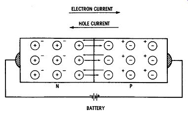
Fig. 10. Electron-hole flow produced
by applied voltage.
... electrons flow from N to P and holes from P to N. The number of carriers taking part in the conduction can be controlled by adjusting the amount of applied voltage. In other words, there will be more current if a higher voltage is applied. This is not so unusual; conductors behave in somewhat the same way. But let us look at an interesting effect which is not true for conductors.
If the voltage applied to this diode junction is in the opposite direction, there will be no current. The applied voltage has the effect of making the wall at the junction higher. In this case, as is shown in Fig. 11, for an electron to travel from N to P, not only would it have to overcome the natural wall at the junction, but it also would have to overcome the voltage of the battery. A PN junction turns out to be a device in which current is allowed in only one direction.
When the applied voltage is of one polarity, the current carriers are given a sufficient push to overcome the wall at the junction. When the applied voltage is of the opposite polarity, the wall at the junction is reinforced and the current carriers find it even harder to move across.
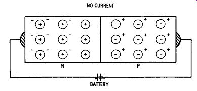
Fig. 11. Zero current flow with voltage applied.
When the applied voltage is of such a polarity as to cause current across the junction, the junction is said to be "forward-biased"; when the applied voltage is of such a polarity as to prohibit current across the junction, the junction is said to be "reverse-biased." The word "bias" indicates that a battery or other voltage source is involved, while "forward" and "reverse" indicate the polarity or direction of the applied voltage.
We have just described a semiconductor diode. The diode is a device which, under normal conditions, allows current in one direction only. Using brute force, it is possible to cause current in the reverse direction. However, this requires the application of a voltage large enough to rip electrons out of the crystal structure. Even this action is useful in the construction of voltage regulation devices, such as zener diodes.
When a junction is reverse-biased, there will be a very small amount of leakage current. This is due to the presence of the minority carriers that are in the material by virtue of the fact that it's impossible to completely exclude them. It is important to note that if somehow we were able to inject minority carriers into a reverse-biased junction, they would immediately go across the junction. For example, the junction in Fig. 11 is reverse-biased, and the majority carriers ( electrons in the N material and the holes in the P material) are forced to stay on their own side of the junction. However, if there are any free electrons present in the P material, they would immediately be conducted over to the N material. The potential wall at the junction would be down hill and the biasing battery would give them an extra push. Actually, this gives us our first insight as to how a transistor works.
PN Junction Characteristic Curve
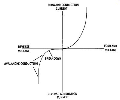
Fig. 12. Characteristic curve for a semiconductor diode.
A curve that shows the relationship between the current through a junction and the voltage applied to it gives valuable insight into the operation of semiconductor junctions. This curve is shown in Fig. 12. Notice that there is no mention of N, P, electrons, or holes on the curve. It deals in terms of voltage and current. Also notice that as the forward voltage increases, the forward current increases.
A point is reached when a further increase in the forward voltage causes the current to rise to a point where the junction may be destroyed. When a reverse-bias is applied to the junction, there is a very small current. This small amount of current is called leakage current. A further increase in the reverse-bias voltage finally causes the junction to break down in the reverse direction, and there is an avalanche conduction in the reverse direction. For some crystals this is not destructive and can be used advantageously. As you will learn later, this is the portion of the curve that describes the action of zener diodes.
The Junction Transistor
(A) NPN transistor.
(B) PNP transistor.
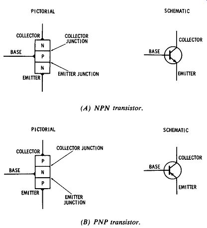
Fig. 13. NPN and PNP transistors.
The transistor is a three-element semiconductor consisting of two junctions. The sandwich is made up of the two types of material (N and P). It can be either an NPN transistor or a PNP transistor. Fig. 13 shows the pictorial and schematic representation of an NPN and PNP transistor. The direction of the arrow on the schematic differentiates between PNP and NPN. The three elements of a transistor are the base, emitter, and collector. The names originated with the idea that the emitter emits the carriers and the collector collects them, while the base is common to both the emitter and collector.
The junction between the emitter and base is called the emitter junction. The junction between the collector and base is called the collector junction.
Controlling the resistance of the transistor is accomplished by controlling the number of current carriers available to the base region.
(C) Complete schematic.
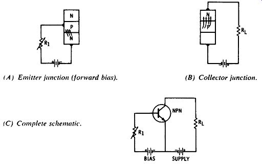
Fig. 14. Transistor bias.
Fig. 14A shows how the emitter junction is forward-biased. By forward biasing the emitter junction, majority carriers flow from the emitter ( N region) to the base ( P region). After these electrons enter the base region, they are no longer majority carriers as far as the collector junction is concerned, they are minority carriers and are conducted immediately through to the collector. Fig. 14B shows how the collector junction is reverse-biased. Therefore, we can control the number of current carriers available to the base by merely adjusting the variable resistor in series with the supply battery. The emitter emits the majority carriers into the base region where they become minority carriers and flow across the reverse-biased collector junction.
Thus, the current applied to the base and emitter controls the resistance of the transistor. This is exactly analogous to the way in which the voltage applied from grid to cathode of a vacuum tube controls its resistance. Fig. 14C shows the equivalent transistor schematic for Fig. 14.
ACTIVE, PASSIVE, LINEAR, AND NONLINEAR COMPONENTS
Every component in the entire field of electronics can be classified as either active or passive, and linear or nonlinear. This gives rise to the comforting thought that there are only four groups of components to consider: passive and linear, passive and non-linear, active and linear, and active and nonlinear. Categorizing semiconductor components in groups of families with similar characteristics will simplify the work of becoming familiar with them. You will be able to associate various devices as having generally the same properties and behaving basically the same way.
Active and passive mean approximately the same thing in electronics as they do in everyday conversation. An active component is one where the output power is greater than the input. In other words, there is a gain connected with the device. For instance, a vacuum tube or a transistor amplifier is considered an active device. An amplifier having an input voltage of 0.2V and an output voltage of 20V would have a voltage gain of 100 associated with it. This would be an active device.
A passive device is one that produces no power increase. Examples of passive devices include resistors, capacitors, inductors, and diodes.
When these devices are used in simple circuits, the output never exceeds the input. For instance, a tapped bleeder across the output of a power supply is nothing more than a common voltage divider, and it serves the purpose of reducing the output to a usable value. This is one example of a passive device.
A linear device or circuit is one at which the output is proportional to the input. In other words, if the input is doubled, the output is doubled; if the input is halved, the output is halved. If the input to a voltage divider is multiplied by 2, the output voltage is multiplied by 2.
If the input voltage is halved, the output voltage is halved. Resistors are a linear circuit component. Other linear circuit components--that is, devices that have an output that is proportional to the input-are linearly operated vacuum tubes, transistors, field-effect transistors, and ( under certain conditions) tunnel diodes and other amplifying devices.
The reason for saying under certain conditions is because transistors and tunnel diodes and most active devices can be either linear or non linear, depending on how they are operated. For instance, a linear amplifier is an amplifier in which the output is proportional to the input.

Fig. 15. AC voltage applied too diode.
A nonlinear device is one in which the output is not proportional to the input. A good example of a nonlinear circuit element is the diode (which conducts current in only one direction). As shown in Fig. 15, when the voltage across the diode is in the forward direction, the output is nearly proportional to the input. But when the voltage across the diode is in the reverse direction, the output is nonexistent. It may help to say that a nonlinear device always distorts the input waveshape.
In the case of a diode, if the input is a sine wave, the output is a half sine wave. Other examples of nonlinear circuit components are capacitors, zener diodes, vacuum-tube diodes, switching transistors, silicon controlled rectifiers, etc. In every case the output is a distorted representation of the input.
To say that a device is nonlinear does not mean that it is bad or not useful. As we shall see, nonlinear devices play very important parts in many areas of electronics. They are used extensively in television receivers, transmitters, computers, etc.
SUMMARY
Semiconductors are solid-state devices.
Germanium and silicon are semiconductor materials that have a crystalline structure.
The process of adding impurity atoms to semiconductor crystals to provide current carriers is called doping.
There are two types of current carriers--electrons and holes.
Electrons are majority carriers in N-type material and minority carriers in P-type material.
Holes are majority carriers in P-type material and minority carriers in N-type material.
Forward bias causes majority-carrier conduction.
A diode junction conducts in only one direction.
For proper operation of a transistor, forward-bias the emitter junction and reverse-bias the collector junction.
A transistor is a variable resistor whose resistance depends on the number of current carriers that are emitted into the base region.
An active component produces gain; a passive component does not.
A linear component produces an output that is proportional to the input.
A nonlinear device distorts the input.