AMAZON multi-meters discounts AMAZON oscilloscope discounts
This section is concerned entirely with passive semiconductor devices. Passive
means that the output from the device is less than the input to it. Both linear
and nonlinear devices will be discussed.
Some of the more important passive semiconductor circuit elements are resistors, thermistors, diodes, breakover diodes, photodiodes, and thermoelectric junctions.
THERMISTORS
Most ordinary resistors are made of carbon or metals. These materials have a positive temperature coefficient; this means that as the temperature increases, the resistance also increases. For example, a resistor having a positive temperature coefficient and a value of 1,000 ohms at 70°F might become 1,050 ohms at 150°F. A thermistor is a resistor with a negative temperature coefficient.
When the temperature increases, the resistance decreases. A thermistor is a piece of semiconductor material that has been doped to provide a given resistance. When the thermistor is heated, the electrons in the crystal gain energy, leave the crystal lattice, and become free current carriers. This means that applying heat to a semiconductor material is equivalent to applying a voltage to it. A big disadvantage of semi conductor circuits is their sensitivity to temperature change. Designers go to great lengths to overcome this temperature problem. In many cases, thermistors are used to compensate transistor circuits for temperature changes.
Thermistors are used to stabilize the effects of temperature variations in various types of circuitry. We have all experienced the annoyance of having to readjust a radio or TV receiver after it warms up. This need for readjustment is due to the change in characteristics of some of the devices in the set after they warm up. Thermistors are used in modem circuitry to compensate for these changes so that this type of adjustment will not be necessary. An example of how this compensation works is that of a series-connected, 1,000-ohm carbon resistor and a 1,000-ohm thermistor. At 70°F, the resistor and the thermistor each has a value of 1,000 ohms; the total resistance is 2,000 ohms. At 150°F, the resistance of the carbon resistor increases from 1,000 ohms to 1,050 ohms. This is a 5 % change in the resistance. At the same time, the resistance value of the thermistor changes from 1,000 ohms to 950 ohms. Even though the resistance of each device has changed, the total resistance remains at 2,000 ohms regardless of the temperature. This basic approach to temperature compensation is used in many types of electronic circuits. Thermistors are particularly useful for stabilizing excessive current flow in power transistors, thus pre venting over-current damage.
DIODES
The diode is a single-junction semiconductor device. The characteristic that makes the diode a valuable circuit element is that it allows current to flow in only one direction. The P-N junction offers a low resistance to current in one direction and a high resistance to current in the opposite direction. Current flow through a diode that encounters a low resistance is said to move in a forward direction; the direction of the high-resistance encounter is called the reverse direction. This gives rise to the terms forward current and reverse current. Reverse current is usually referred to as leakage current because it is an undesirable characteristic.

Fig. 1. Schematic and pictorial symbol for a diode.
Fig. 1 shows the schematic symbol for the diode. The bar represents the cathode, and the arrow represents the anode. Fig. 2 shows how to bias a diode. It is forward-biased (for maximum current flow) when the anode is positive and the cathode is negative. It is reverse-biased (for minimum current flow) when the anode is negative and the cathode is positive.
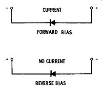
Fig. 2. Polarity of voltage for forward and reverse bias.
As the forward bias applied to diode is increased, the current will increase to the point where excessive heat will damage the junction.
When a diode is reverse-biased, current is blocked from flowing through the junction. If the reverse voltage is sufficiently increased, the diode will break down and in most cases the excessive current will destroy the junction.
The two most important characteristics of a diode are the maximum forward current and the maximum reverse voltage that the diode can withstand. The maximum forward current is an indication of how much current the diode can carry before it is damaged. The maximum reverse voltage indicates how much reverse voltage the unit can block before it breaks down. Exceeding either of these ratings will usually destroy the diode.
Rectifiers The most common use for diodes is to convert alternating current into direct current. The diode is a nonlinear device that fits this task perfectly (Fig. 3A). Since it passes current in only one direction, it clips off the negative half of the sine wave, leaving only the positive half. This produces a choppy DC, but since all the pulses go in the positive direction, it can be considered as pulsating direct current.
These pulses can be smoothed, as shown by Fig. 3B. This figure shows the addition of a simple capacitor that makes up a filter.
The purpose of the resistor is merely to complete the circuit and provide a load for the diode. As the input signal goes positive, the diode is forward-biased and is nearly a short circuit. Thus, the input voltage appears across the load resistor. When the input voltage goes negative, the diode is reverse-biased and is nearly an open circuit; therefore, none of the input voltage is passed to the load resistor. The resulting waveshape is shown in Fig. 3A at the output of the half-wave rectifier.
(A) Rectifier section. (B) Filter section.
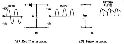
Fig. 3. Diode rectifier and filter.
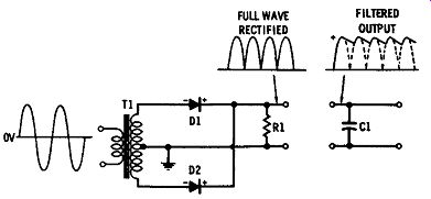
Fig. 4. Full-wave rectifier.
A capacitor is placed across the load resistor to filter the ripple in the DC output. The capacitor stores energy by charging when a voltage is applied and then releasing this energy into the circuit when the charging pulse is removed. Thus, during the negative half cycle when the diode is blocking the input voltage, the capacitor is discharging into the load resistor, giving the effect of smoothing the output DC waveshape (Fig. 3B). It is possible, by using two diodes and a transformer as shown in Fig. 4, to obtain twice as many output pulses, thereby improving the regulation of the DC output voltage. This is called full-wave rectification. When the input voltage goes positive, the transformer causes diode Dl to be forward-biased and the positive half cycle appears across the load resistor. When the input signal goes negative, diode D2 is forward-biased, causing the negative half cycle to appear across the load resistor. The circuit is built so that both diodes conduct in a manner that produces the same polarity of voltage across resistor R1 in Fig. 4. This has the effect of converting the negative half cycle to a positive one. The center-tapped secondary of the transformer puts each diode into a separate circuit. When one diode is forward-biased, the other diode is reverse-biased. Thus, there is conduction on both halves of the input cycle, and full-wave rectification results.
Fig. 5 shows another method of constructing a full-wave rectifier.
This is called a bridge rectifier because the diodes are connected in the form of a square and the input and output terminals are at opposite diagonals of the square. When the applied AC input voltage is positive,
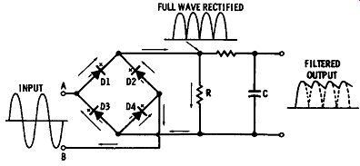
Fig. 5. Bridge rectifier.
D1 and D4 are forward-biased and D2 and D3 are reverse-biased.
Current flows from A ( + with respect to B) through D1, through the output circuit, through D4, and back to the B terminal at the input.
When the input voltage is negative, D2 and D3 are forward-biased and D1 and D4 are reverse-biased. Current flows from B through D2, through the output load resistor, and through D3 to input terminal A. It can be seen from this diagram that the current of both positive and negative alternations flows in the same direction through the load resistor; this provides full-wave rectification. If a filter network is placed across the load resistor of a bridge rectifier, the output will be filtered to produce a nearly smooth DC. At first glance you might think that a bridge rectifier has a definite disadvantage in that it requires more diodes for full-wave rectification than the previous power-supply example. The truth of the matter is that the bridge rectifier is probably less expensive than the other, because the bridge rectifier does not require a transformer to accomplish full-wave rectification. In addition, the diodes can have a lower voltage rating, since in each conduction path there are two diodes rather than just one, as in the case of the transformer circuit. This means that under conditions of reverse bias, two diodes will divide the reverse voltage that they must block. If the voltage to the diodes is 200V peak-to-peak, the diodes of the bridge rectifier need only be capable of blocking 100V each; whereas in the transformer-type rectifier system, the single diode must be capable of blocking the entire 200V. Diodes are widely used in power-supply circuits to rectify AC signals.
Semiconductor diode circuits are designed in the same manner as vacuum-tube diodes; however, they have advantages in that they require no heater voltages and take up very little space compared to vacuum tubes. They can be designed to carry· very high forward currents and to withstand large reverse voltages.
Breakdown Diodes
The breakdown diode is more commonly known as the zener diode.
The word breakdown, or avalanche, is more descriptive because it actually indicates what happens inside the zener diode, which is a passive, nonlinear semiconductor. Fig. 1-12 in Section 1 shows that when a diode is sufficiently reverse-biased, a point of breakdown is reached. This action damages most diodes, but it was found that silicon diodes could be used to great advantage at this point. Fig. 6 is an expanded view of the reverse-bias portion of a silicon-diode characteristic curve. Notice that for a small change in reverse voltage a large change occurs in the reverse current. At this point the voltage across
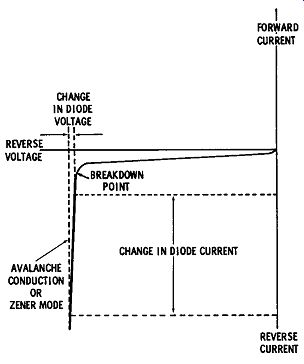
Fig. 6. Breakdown diode characteristic.
the breakdown diode is nearly independent of the zener current. The breakdown diode can therefore be used to regulate voltages. That is, it can be used to hold voltages constant regardless of the amount of current drain.
Fig. 7 shows the circuit of a breakdown-diode voltage regulator.
When the zener diode is forward-biased, it behaves as a normal diode, but when it is caused to break down in the reverse direction, the voltage across it remains constant even when there is a change in the current or applied voltage. To take advantage of its voltage-regulating ability,...
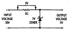
Fig. 7. Zener voltage regulator.
...the zener diode must be biased in a manner opposite that of a normal diode. Zener diodes are specified in terms of their breakdown voltage.
In other words, a 5-volt zener would maintain a voltage of 5 volts when broken down in the reverse direction. If the input voltage to the regulator circuit were 10 volts, there would be 5 volts across the breakdown, or zener, diode and 5 volts across the resistor. If the input voltage were to rise to 15 volts, there would still be 5 volts across the zener diode and 10 volts across resistor R1. This zener-diode circuit maintains the output voltage at a constant 5 volts, regardless of the input voltage changes.
The zener diode can be used for many purposes, one of which is regulating the output voltage of DC power supplies for transistor circuits. For instance, consider the 30-volt transistor power supply...
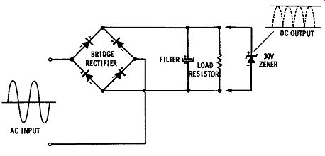
Fig. 8. Regulated power supply.
...shown in Fig. 8. Without the zener control, the output voltage of this power supply would change with input voltage fluctuations and load changes. It would be considered a poorly regulated power supply.
If the nature of the transistor circuit it is supplying is such that it cannot tolerate these fluctuations, the regulation may be improved by the addition of a proper breakdown diode. In addition to the regulating action, the addition of the breakover diode decreases the ripple in the final DC output.
Another example of a circuit where zener diodes are used is in the generation of square waves. The zener circuit for producing square waves is shown in Fig. 9. The function of the normal diode (D1) is to remove the negative half of the sine wave. The positive half cycles have a peak of 15 volts. The zener diode breaks down at 5 volts, thus shorting out the peak of the input signal. The resultant output wave shape is nearly a square wave. Square-wave pulses of this type are used in many electronic circuits, such as those in computers, radar systems, and television receivers.
Diode Gates

Fig. 9. Square-wave generator.
Thousands of diodes are used in the electronic gating circuits of modem digital computers. A gate is a device that has an output only if certain input conditions are satisfied. It can be compared to an ordinary fence gate that opens if certain input conditions are fulfilled.
When the gate is unlocked and nothing is standing in the way, the gate opens if someone pushes on it. Suppose, in a certain computer, we want to turn on a front-panel indicator light when: the motor is on, the computer is not performing a specific operation, and the operator pushes a certain button. This function would be performed by a gate.
Voltages at the input of this gate indicate when all three of these pre requisites are fulfilled. When all three voltages are present, indicating that everything is ready, the gate opens and there is an output which turns on the lamp.
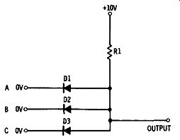
Fig. 10. AND gate.
The lighting of the lamp mentioned in the previous paragraph can be accomplished by using an AND gate. If the three conditions are considered as A, B, and C, we can say that when the voltages are present for A and B and C, then there will be an output to turn on the lamp--thus the name AND gate. Fig. 10 shows a diode AND gate. Notice that when the input voltages to the diodes are at zero, current flows from + 10, through resistor R1, and through the diodes.
The forward-biased diodes can be considered as short circuits. There fore, when all zeros are present at the input of the diodes, the output will be zero because it is shorted through the conducting diodes to the input "zeros." In this case, no voltage indicates that conditions A and B and C are not present, and the gate is closed. If one of the inputs is raised to + 5 volts, the corresponding diode has less forward bias and does not conduct as heavily. However, each of the other two diodes is still strongly forward-biased and will continue to short the output to zero volts. This is merely saying that fulfillment of one input condition is not enough to cause the gate to open. Should two of the + 5-volt inputs be present, the output would still be shorted out by the third conducting diode, and the output would still be zero. The conditions for opening the gate have not yet been fulfilled. If all three input voltages are raised to + 5 volts, all three diodes have less forward bias and the output will be connected to the three + 5-volt inputs through the diodes. This voltage will then be used to turn on the lamp.
The output voltage will rise only when all three input conditions are fulfilled. Only when A and B and C are present will there be an output voltage.
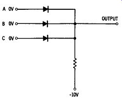
Fig. 11. OR gate.
Suppose you want to turn on the output lamp of the computer when any one of the input voltages is present. You would want the presence of either A or B or C voltage to turn on the output lamp. This would require an OR gate. An OR gate is one where any input being present will turn on the output. A diode OR gate is shown in Fig. 11. In this case, all diodes are again forward-biased. When zero voltage is present at all inputs, the output voltage is zero because it is connected to the zero-volt input through the conducting diodes. If the A input voltage rises to + 5 volts, the corresponding diode becomes more forward biased and the output is shorted to the + 5 volts through the more heavily conducting diode. The input voltage is conducted through the diode to the output, even though the B and C inputs remain at the zero level. The same action will be repeated if any of the other inputs are turned on. If A or B or C is present at the input, there will be an output.
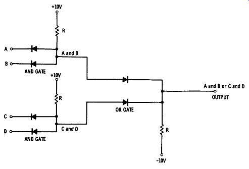
Fig. 12. Logic circuit.
Fig. 12 shows a combination of two AND gates and one OR gate used to accomplish a single logic function. Diodes are popular because they are relatively inexpensive, high switching speeds can be attained, and the circuitry simplifies the problem of designing, maintaining, and servicing the equipment.
Photodiodes
Current carriers in semiconductors are sensitive to many different types of energy. In the case of thermistors, the semiconductor is sensitive to heat energy. Light energy may also be used to excite electrons so that they will move out of the crystal structure and enter into conduction as current carriers. A photodiode is one of a group of such devices.
It is a straightforward PN junction, having a plastic lens in the top of the container through which light can reach the junction.
When used in a circuit, this type of diode is biased in the reverse direction. When the semiconductor junction is exposed to light, energy

Fig. 13. Photodiode.
is absorbed by the electrons; the energy they gain permits them to overcome the junction potential, and the diode conducts in the forward direction. One might say that the energy of the light is used to overcome the barrier produced by the PN junction. Fig. 13 shows a sketch of a typical photodiode. It is contained in a case similar to that in which a transistor is packaged. The top contains a lens through which the light passes. Fig. 13 also shows the schematic symbol for a photo diode. The small arrows indicate impinging light.
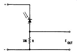
Fig. 14. Circuit for indicating light intensity.
The diagram in Fig. 14 shows a photodiode circuit used for measuring light intensity. When no light illuminates the diode, no current flows in the circuit and thus the output voltage is zero. The photodiode conducts when light hits it. Its resistance decreases by an amount that depends on the intensity of the light. Therefore, the current through R and the output voltage are controlled by the intensity of the light.
THERMOELECTRIC COOLING
Semiconductor materials are also beginning to find wide application as heat pumps. This means that they can accomplish the same tasks that a refrigerator performs. Refrigerators are already employing semi conductor materials as heat pumps instead of the standard compressor and motor. Fig. 15 shows a typical semiconductor thermocouple.

Fig. 15. Semiconductor thermocouple.
The principle is based on the fact that when an electron goes from a low-energy state to a high-energy state, it must absorb energy. The electrons in N-type material are plentiful and therefore are in a high energy state, whereas in the P-type material the electrons are in a relatively low-energy state. Thus, when an electron travels from P-type material to N-type material, it absorbs heat energy from the surroundings, which are, as a result, cooled. On the other hand, when electrons go from a P-type material to N-type, they give up energy and thus dissipate heat. This is what happens when the electrons leave the material and go to the hot surface copper strap through the battery back to the N-type. The net result of the entire system is that the top copper strap is cooled while the lower one is heated. The heat is pumped from the cold surface to the hot. This does not violate any of the laws of thermodynamics. Heat that is pumped from the cold side of the junction and all of the energy must be dissipated by the hot junction. The most common means of dissipating this heat is by using a heat sink. In actual application the thermoelectric cooler is sandwiched between the cold plate and the heat sink, as shown in Fig. 16, which illustrates the sandwiching of multiple thermocouples ...
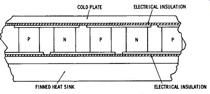
Fig. 16. Multiple thermocouples.
... to form a refrigeration system. It is also possible to reverse the flow of current and produce a reversal of the hot and cold surfaces.
One of the applications of thermoelectric coolers at the present time is as an improved heat sink for power transistors. The cooling effect is used to maintain a low case temperature for the transistor and thereby increase the power-handling capabilities of the transistor.