AMAZON multi-meters discounts AMAZON oscilloscope discounts
Conventional closed-loop regulator circuits employ losser elements controlled by amplified error signals. The error signals are derived from a portion of the output voltage or current that has been compared to a stable voltage reference.
This approach is a good one, for regulation and dynamic output impedance can readily be improved by simply increasing the gain imparted to the error signal. Large amounts of power can be regulated, and only negligible power need be dissipated in the reference element. Despite this, impelling reasons exist for resorting to modified circuit techniques to attain the same objective. DC amplification, for example, is inherently a difficult process because of the drift from cascaded stages. Another shortcoming of the conventional approach to closed-loop voltage or current regulation is that the losser element must dissipate considerable power. This greatly reduces the over-all efficiency of the regulated power supply and necessitates some means of heat removal. Heat removal rapidly becomes a design limitation where large capacity supplies must be confined within a reasonable cabinet space. Still another obstacle is the design of solid-state supplies capable of reliable performance above several dozen volts. The losser transistor then becomes increasingly susceptible to destruction from shorts and transients. For these and other reasons, we will now investigate regulated power supplies which, although of the closed-loop species, deviate significantly from the circuits presented previously. Final discussion will deal with auxiliary circuits for protecting series losser regulation from destructive overload effects.
CHOPPER STABILIZED SUPPLIES
The problem of obtaining high loop gain of the error signal, without the accompanying drift which characterizes DC amplifiers, can be solved by wholly or partially dispensing with DC amplification. In order to do this, the DC error signal must be converted to AC or pulses to which high gain can be imparted by stable AC amplifiers. After amplification, the relatively high-level error signal is rectified, filtered, and then applied to the control electrode of the conventional series losser element. Although this basically describes the technique of substituting AC for DC amplification, an important consideration remains-merely converting the DC error signal to AC permits the use of AC amplification, but at the same time destroys sensing of the phase or polarity of the original DC error signal. As a consequence, unless polarity sensing is somehow recovered or restored, the losser element will receive a control signal which can just as readily cause the output-terminal voltage to change in the opposite direction required for compensation. Hence, some form of synchronous rectification or DC restoration must be introduced at the output of the AC amplifier. This is done so that positive or negative DC control (whichever is needed ) can be fed to the losser element to counteract the changes in line voltage or load current.
How this important function is accomplished can be grasped by studying the schematic diagram of Fig. 6-1.
Here, transistors X1 and X2 produce AC amplification of the interrupted, or "chopped," error signal. Transistor X3 provides subsequent DC amplification. Transistor X4 is the familiar emitter follower which drives series losser transistor X5. Although there are three cascaded direct-coupled stages, the DC drift is negligible for two reasons : First, the DC amplification is much lower than the preceding AC amplification. Secondly, the relatively low DC amplification takes place after the error signal has been boosted by the AC amplifier. X3 is the only DC voltage-amplifier stage.
In addition to being the first AC amplifier stage, X1 also performs as a zero sensing element. In this function X1 is analogous to the circuitry position occupied by the first DC amplifier stage in conventional regulators-that is, those employing DC amplification throughout. Let us consider the situation at point Y, the base of transistor X1 (Fig. 6-1). When the chopper armature is not at position B, the 12-mfd capacitor connected to the base of X1 is charged to the voltage sampled from the DC output terminals of the supply.
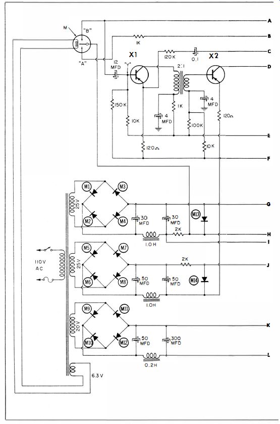
Fig. 6-1. A chopper stabilized voltage regulator rated at 12 volts and
1 ampere.
When the chopper armature is at B, however, the positive reference voltage derived from zener diode M13 is connected to the positive plate of the 12-mfd capacitor. If, then, the stored charge from the output terminals has produced a higher voltage in this capacitor than the voltage from the reference source, a partial discharge must occur. This results in a negative pulse at point Y. If the voltage sampled from the output terminals is lower than the voltage sampled from the voltage reference source, this capacitor must receive an additional charge, thereby producing a positive pulse at point Y. When the two sampled voltages are the same, no change in charge condition is imposed on the 12-mfd capacitor and no error signal appears at point Y. The amplified error signal, when it exists, appears as a relatively high positive or negative pulse (or pulses ) at point S. More specifically, it appears at point X when the chopper armature is at position B. When the chopper armature is at position A, point X receives the positive reference voltage from zener diode M13. Capacitors C1 and C2 are the storage elements of a low-pass filter, the function of which is to present the base of X3 with a fairly low-ripple DC bias despite the cyclic fluctuations appearing at point X. Residual ripple then tends to be electronically filtered by the regulating action of the circuit. The DC bias at the base of X3 is varied, by the process just discussed, in such a direction that the terminal voltage change responsible for the error signal is counteracted. It can readily be appreciated that, without the position-A function of the chopper, X3 and consequently series losser X5 would not be informed which way to change conduction in order to correct the terminal voltage. Table 6-1 contains the component data for the chopper circuit in Fig. 6-1.

Table 6-1. Component data for circuit in Fig. 6-1

Fig. 6-2. Basic configuration of a transistor chopper.
There are other ways to apply electromagnetic choppers for the basic purpose of modulating the error signal. Furthermore, the DC-to-AC conversion can be accomplished by either vacuum tubes or transistors, as shown in Fig. 6-2.
However, this power supply is representative of the objectives attained by providing for AC amplification within the feedback loop. The inference should not be drawn that so-called "chopper-stabilized" amplifiers or power supplies derive their stability from the chopper-in the same sense that negative feedback confers stability, for example. The enhanced "stabilization" comes about because the chopper permits dispensing with at least a major portion of the DC amplification, which would otherwise be required to produce the same over-all loop gain. Theoretically, the chopper amplifier cannot respond more rapidly than the duration of a half-cycle of the chop frequency. In most practical applications, the response time is a small fraction of this time because of the low-pass filter network generally employed to attenuate the AC components from the demodulated or rectified output. Consequently, regulated power supplies with chopper-stabilized amplifiers tend to exhibit slow response times. Because of the high loop gain provided by AC amplification, however, they are characterized by an extremely low dynamic output impedance within their frequency response.
CONVERTER-TYPE VOLTAGE-REGULATED POWER SUPPLY
The voltage-regulated supply of Fig. 6-3 is designed around a DC-to-DC converter involving essentially power transistors X1 and X2 and saturating transformer T1.
Although a 12-volt battery is depicted, a suitable rectifier and-filter arrangement could be substituted to provide operation from the AC power line. Briefly, the transistor which happens to conduct first when the switch is closed thereby induces voltages in the tapped transformer winding. As a result, conduction simultaneously increases in that transistor and drives the alternate transistor into non-conduction.
The current through the emitter-to-collector circuit of the conducting transistor rapidly attains a saturation value beyond which the emitter-to-collector resistance can decrease no further. The current through the portion of the transformer winding involved with the conducting transistor will, however, continue to increase until the transformer core becomes magnetically saturated. When this occurs, the prevailing regenerative cycle of events is abruptly halted, since the electromagnetic induction is insufficient to develop the voltages necessary to maintain forward-conduction bias to the conducting transistor and cutoff bias to the nonconducting transistor.
A rapid collapse now takes place, with the transistors alternating their conduction roles. The collapse is regenerative because once it has started, the reversed voltages now bias the respective transistors in the direction favoring the switching action. The alternate transistor is now switched on, remaining on until saturation of the core again initiates a new half-cycle. A square wave is generated, and the process is extremely efficient because of the low saturation resistance of the transistors and the rectangular hysteresis loop of the transformer core. Ordinary transformer action in the secondary winding then changes the generated voltage to some desired value.
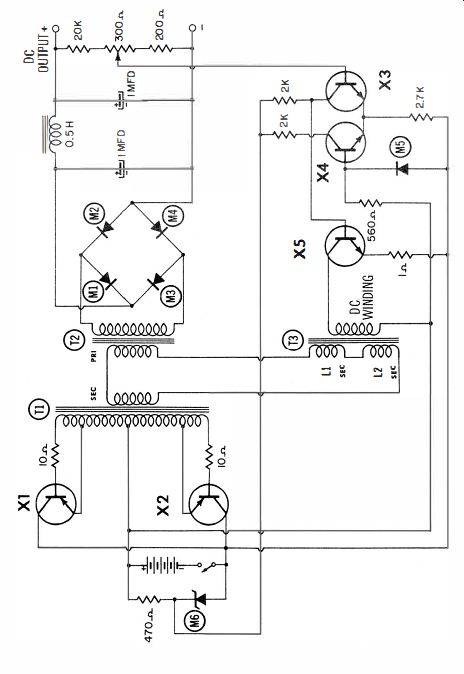
Fig. 6-3. A converter-type voltage-regulated power supply.
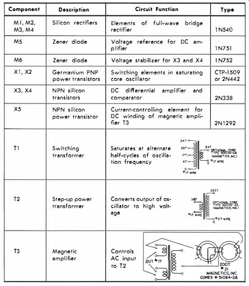
Table 6-2. Component data for circuit in Fig. 6-3
The AC developed in the secondary of transformer T1 is converted to DC by the rectifying circuit comprising power transformer T2, the silicon diode bridge, and the associated filtering components_ Notice, however, that the secondary windings of T3 are inserted between transformers T1 and T2. T3 functions as a magnetic amplifier, or saturable choke, in which the magnetizing current supplied to the DC winding is controlled by transistor X5. X5 is actuated by the error signal produced by the differential amplifier (X3 and X4), in response to a portion of the DC output voltage and to the reference voltage developed by zener diode, M5.
Regulating action is such that transistor X5 is driven harder into conduction when the DC output voltage tends to fall, thereby bringing the core of T3 more into its region of magnetic saturation. This is accompanied by decreased inductance in AC windings L1 and L2, permitting more AC voltage to be impressed across the primary winding of T2.
In this way, the DC output voltage is restored to its nominal regulated value. If the DC output voltage tends to rise, the converse sequence occurs.
Although optimum design for T3 generally involves a measure of experimental work, the above method of regulation has the outstanding feature that the transistors are isolated from high voltage. Also, an accidental short across the output of this supply will kill oscillation but should not damage any components. (Table 6-2 gives the parts data for this circuit. )
VOLTAGE REGULATION WITH SILICON CONTROLLED RECTIFIERS
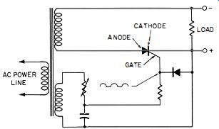
Fig. 6-4. Half wave silicon controlled rectifier (SCR) supply with phase
shift adjustable gate signal.
The silicon controlled rectifier is the solid-state counterpart of the thyratron. Like the thyratron, it permits the varying of a current through it by changing the phase (time of occurrence ) of the signal applied to a control electrode.
In thyratron fashion, once conduction is initiated the control electrode loses control ; conduction is extinguished as the AC voltage passes through zero. Fig. 6-4 depicts a simple circuit employing a silicon controlled rectifier to provide half-wave rectification. The control electrode, or gate, is supplied with a small voltage from a phase-shifting network. No conduction takes place through the rectifier until the gate potential reaches a certain value. The time required to reach this value is a function of the phase difference between the gate-cathode and anode-cathode voltages. If the phasing is such that conduction is established early in the positive excursion of the AC voltage impressed between anode and cathode (Fig. 6 5A), the duty cycle of the rectified pulses will be relatively high and so will the average DC output voltage.
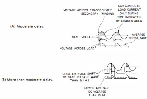
(A) Moderate delay. (B) More than moderate delay.
Fig. 6-5. Effect of gate firing voltage delay on average DC output of circuit in Fig. 6-4.
The converse is true in Fig. 6-5B, where the phasing of the gate signal holds off conduction until the positive excursion of the anode-cathode voltage is nearly completed. (In this simple arrangement, the positions of the variable resistance and the capacitor would have to be interchanged to obtain the amount of phase shift indicated in the waveform diagrams. However, this does not invalidate the basic principle under investigation.) We see at once that control of conduction time is much more efficient than using variable losser elements to vary the output current and/or voltage. While the silicon controlled rectifier is conducting-whether for a tiny or a major portion of the impressed half-cycle-the power wasted in the device itself is negligible because saturation exists, regardless of the duration of conduction. Conduction is always at or near maximum, or not at all ; consequently, the PR losses in a silicon controlled rectifier are very low. This greatly relieves the thermal problem, a major design and operational headache when power transistors are used as losser elements in conventional voltage-regulator circuits.
To impose automatic voltage regulation on a silicon controlled rectifier supply; it is necessary to insert a circuit or device into the feedback path to shift the phase (vary the time of occurrence ) of the gate signals in response to an error signal . A relaxation oscillator, involving a unijunction transistor, provides this requisite with a minimum of components. Fig. 6-6A shows a unijunction relaxation oscillator and Fig. 6-6B a somewhat analogous circuit employing the more familiar neon bulb. In both instances, a capacitor (C1) is connected across the electrodes, which abruptly change from an open to a closed circuit when the voltage across the capacitor has charged to a certain value. In the neon bulb, this event is brought about by the onset of ionization, which changes the gas from an insulator to a conductor. In the unijunction transistor, the switch from the nonconductive to the conductive state is the result of a change from reverse to forward bias across a PN junction. Fig. 6-7 shows the unijunction transistor. It consists of an N-type silicon bar with ohmic contacts established at the ends, at B1 and B2.
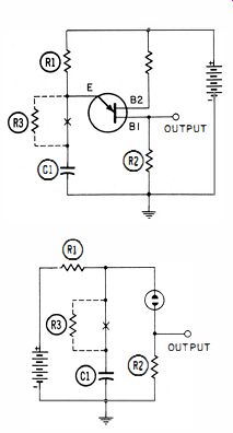
Fig. 6-6. Relaxation oscillators.
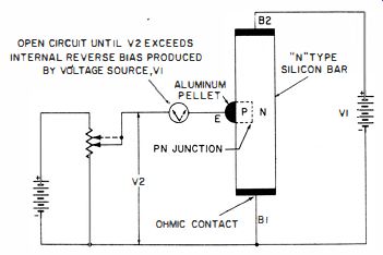
(A) Unijunction transistor circuit (B)
Neon-bulb circuit. Fig. 6-7. Circuit for demonstrating switching of conductive
states in unijunction transistors.
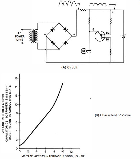
Fig. 6-8. Triggering characteristics of the unijunction transistor. (A)
Circuit. (B) Characteristic curve.
(This device used to be called a double-base diode. ) P-type semiconductor material is alloyed or diffused to the central portion of the bar to form a PN junction. If a current is passed between B1 and B2 by voltage source V1, the voltage distribution within the silicon bar will be such that the PN diode between E and B1 will be reverse-biased. As a result, no current can flow through the diode unless voltage source V2 is high enough to overcome the reverse bias.
It is important to realize that the presence of a resistance such as R3, in either the neon bulb or the unijunction oscillator of Fig. 6-6, will slow down the repetition rate of the pulses. The reason is that R3 forms a voltage divider (in conjunction with R1) and thereby reduces the voltage applied to capacitor C1. Under this condition, C1 requires a longer charging time to attain the firing potential for its associated device. This property is readily exploited to vary the timing of the gate signal of silicon controlled rectifiers.
Another useful characteristic of the unijunction relaxation oscillator is revealed by Fig. 6-8. Note that the capacitor voltage required to trigger the device is a function of the voltage applied across contacts B1 and B2 (Fig. 6-8A). In particular, if the latter voltage is removed, a fraction of a volt across capacitor C1 will suffice to establish forward conduction in diode section E-B1 (Fig. 6-8B). As a corollary of this relationship, it follows that removal of the Bl-B2 voltage will cause forward conduction in the E-B1 diode whenever the capacitor voltage is more than a fraction of a volt. Thus, in the circuit of Fig. 6-8A the relaxation oscillator, regardless of its free-running repetition rate, is synchronized to the 60- hz power line in such a way that the generation of pulses must begin anew every 120th of a second.
A complete circuit of a controlled-rectifier voltage-regulated supply is shown in Fig. 6-9. A synchronized unijunction oscillator provides the gate signals. Transistor X1 is actuated from an error signal derived from the difference between the reference voltage across zener diode M6 and a sampled portion of the power-supply output voltage. The error signal controls the effective base-to-collector resistance of X1 (which, for practical purposes, is shunted across the 0.25-mfd charging capacitor ). Should the DC output voltage tend to rise, the emitter of X1 will be biased further negative with respect to its base. Since X1 is an NPN transistor in a common-base configuration, it conducts more heavily-that is, the effective resistance represented by the collector-to-base diode is decreased. The 0.25-mfd capacitor then takes longer to attain the potential it needs to fire unijunction transistor X2. This, in turn, delays firing of that silicon controlled rectifier, which is properly polarized from power transformer T1. In alternate half-cycles of the line frequency, the firing of the opposite silicon controlled rectifier is similarly delayed. Because the conduction current in the two silicon controlled rectifiers has been reduced to smaller portions of a half-cycle, a lower average DC current flows to the filter and load (Fig. 6-10) . This is manifested as a reduction in DC output voltage, which counteracts the voltage rise responsible for the corrective error signal. The converse sequence of events occurs whenever the output voltage tends to fall (see Fig. 6-11 ). The power amplification realized in this type of error-sensing circuit can be extremely high.
Component data for the circuit of Fig. 6-9 are given in Table 6-3.
DC SWITCHING-TYPE VOLTAGE REGULATOR
Duty-cycle modulated pulsing of the output of a DC power supply is a circuit technique which holds considerable promise for more efficient operation than can be attained from a conventional losser regulator, wherein the resistance of the losser element is varied to compensate for any change in output voltage. A block diagram of a voltage regulator employing the pulsing or DC switching principle is shown in Fig. 6-12, and the schematic appears in Fig. 6-13. The parts data for this circuit are given in Table 6-4. The significant feature of this supply is that the variable-resistance characteristic of the series losser is replaced by a type of switching action whereby the load current is either fully on or fully off. The average load current-therefore, the value of the filtered output voltage-depends on the ratio of time on to time off.
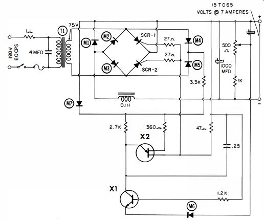
Fig. 6-9. Silicon controlled rectifier (SCR) voltage regulated supply using
variable conduction time technique.
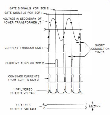
Fig. 6-10. Conditions in circuit of Fig. 6·9 when phasing of gate signal
allows short conduction time.
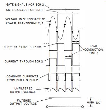
Fig. 6-11. Conditions in circuit of Fig. 6·9 when phasing of gate signal
al lows long conduction time.

Table 6-3. Component data for circuit in Fig. 6-9
(A) CONTROL SIGNAL SUPPLIED TO ELECTRONIC SWITCH WHEN OUTPUT VOLTAGE IS AT NOMINALLY REGULATED VALUE. ( B) CONTROL SIGNAL SUPPLIED TO ELECTRONIC SWITCH WHEN OUTPUT VOLTAGE FALLS (C ) CONTROL SIGNAL SUPPLIED TO ELECTRONIC SWITCH WHEN OUTPUT VOLTAGE RISES.
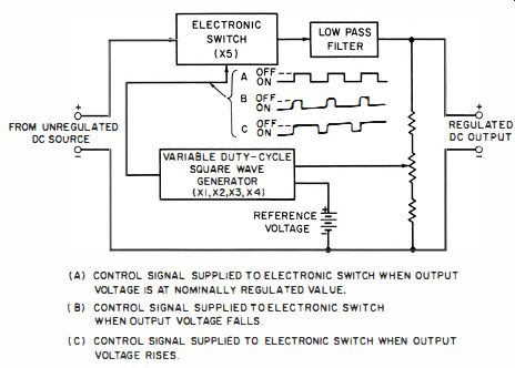
Fig. 6-12. Block diagram of DC switching regulator.
It is this ratio which is varied by the error signal. If the output voltage rises, less "on" time is produced-to the extent that the voltage is nearly restored to its nominal regulated value. The converse events occur if the output voltage falls. When the switch is on, its resistance is ideally zero and, practically, quite low. Therefore, the PR loss in the ...
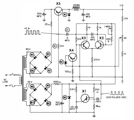
Fig. 6-13.
Schematic of typical DC switching type voltage regulator with an 50-volt,
500-milliampere output rating.

Table 6-4. Component data for circuit in Fig. 6-13
... switching element is relatively small. The thermal problem is considerably relaxed with respect to a conventional losser regulator of like capacity. This type of supply has another advantage-high-gain DC amplification is not required for the error signal.
In the schematic diagram of Fig. 6-13, transistors X2 and X3 are connected as a single-shot multivibrator which, not being free-running, is repeatedly being triggered through its cycle by sharp pulses which have been derived from the unijunction relaxation oscillator X1. The duration of the multi vibrator output pulses is then controlled by transistor X4, which acts as a variable resistance in the base-to-emitter circuit of X3. The total effective resistance of the collector to-base circuit of X4 is governed by the error signal at the emitter of X4.
The output pulses generating from the multi vibrator are transferred, through capacitor CI, to the base of switching element X5. Transistor X5 is forward biased by resistor RI in its base lead, but is turned off while positive pulses are being supplied from the multivibrator. Consequently, the ratio of "on" to "off" time of transistor X5 is controlled by the duty cycle of the multivibrator. Inasmuch as the switching rate of this network is relatively high (approximately 1 khz in this circuit) , the response time is not limited by the power-line frequency, as it is in the AC switching regulator such as the phase-control SCR supply in Fig. 6-9.
Diode M1 provides a current path through which the stored energy in the filter choke can safely dissipate itself when the switching element is turned off. This produces a flywheel effect which contributes to filtering action. Without M1, the emf developed across the choke, when X5 is switched off, could destroy the transistor.
OVERLOAD PROTECTION FOR SERIES LOSSER VOLTAGE REGULATORS
Some words are now in order with regard to the protection of solid state regulated supplies from the effects of short circuits. The transistor used as the series losser is often far from being an inexpensive item. Yet, this circuit element is extremely vulnerable to damage from over-current (and over-voltage in some cases ). In some of the higher voltage supplies, the situation is aggravated by the fact that the output terminal voltage exceeds the safe collector-emitter voltage. This operational mode is perfectly satisfactory when a normal load is being powered ; the voltage dropped across the series losser need be only a relatively small fraction of the voltage actually available from the rectifier-filter circuit. Such a voltage drop can be safely within the allowable ratings of the losser transistor. However, the occurrence of a short circuit at the output terminals of the regulator immediately places the rectifier output voltage across this transistor. Obviously, some investment of time and money in protective techniques becomes worthwhile in those instances where short circuits are probable. This certainly pertains to laboratory supplies used for experimental and developmental purposes.
The deployment of the control transistor as a shunt, rather than a series losser element neatly circumvents the short circuit problem. A short circuited shunt regulator is deprived of its voltage and thus automatically removes the shunt control transistor from danger. (A continued over-current situation can, of course damage the series resistance or components in the rectifier circuit ). However, the very low efficiency of the shunt regulator when delivering low-load current tends to lessen its popularity. Considerable protection can be conferred upon the generally more efficient series type regulator by making use of appropriate design philosophies and circuit techniques.
Where feasible, the use of larger than necessary germanium power transistors sometimes constitutes a big step in the right direction. Such transistors tend to be inexpensive and, when suitably heat-sinked, display relatively long thermal time constants. This decreases the likelihood that a momentary short circuit will damage the transistor. Moreover, it is only with such large transistors that fuses can provide a measure of protection. Actually, the basic problem is centered about the difficulty of preventing transistor damage during the interval in which the fuse is responding to a condition of overload. It is, in most cases, best to incorporate some means of protection which asserts itself more rapidly than the many tens of milliseconds involved in blowing a fuse with excessive current.
Such protection can be obtained by incorporating semi-conductors switching devices which have completed an evolutionary phase not unlike that of the first decade following the introduction of the junction transistor. The products now available are characterized by a high order of reliability, refinement in characteristics, and wide variety of ratings. These devices find useful application in protective circuits associated with series losser regulators. They have also been successfully employed in regulators based on switching or phase-shift control techniques. Four types appear to have met widespread approval from circuit designers. These are : the silicon-controlled rectifier (SCR) , the silicon controlled switch, the gate-turn off switch, and the controlled AC switch.
The general device characteristics of the silicon-controlled rectifier and the silicon-controlled switch are similar. Both lose gate control of forward conduction current when once turned on in DC circuits. Turn-off must be accomplished in both devices by momentarily bringing about a drastic decrease or an interruption in forward conduction current.
(This is automatic in AC circuits due to the passage of the AC wave through zero.) Turn-on in both devices is accomplished by a tiny amount of power relative to the power passed to the load. The silicon-controlled switch is fabricated of two transistor-like structures, whereas the silicon-controlled rectifier utilizes a four-layer, three-junction construction. The application-oriented difference between the two devices involves the fact that the silicon controlled rectifier is made in larger current carrying capacities than is the silicon-controlled switch. The former switching device is generally used in circuits where current flow ranges from about one-quarter ampere to hundreds of amperes. The latter performs similar switching functions where the current flow ranges from tens to hundreds of milliamperes.
Typical General Electric silicon-controlled switches are listed in Table A-12 in the Appendix. Table A-13 (also in Appendix) shows a portion of a large number of silicon controlled rectifiers made by the same manufacturer.
Unlike the two aforementioned switching devices, the silicon gate turn-off switch retains gate control of its forward conduction current in both DC and AC circuits. Its use has merit in high efficiency regulated supplies based on series-switching of one DC line. Output voltage or current control of such supplies is achieved by changing either the duty cycle or the switching rate in response to an error signal generated by a change in output. A drawback of these devices is that the turn-off gate power is much greater than the turn-on gate power. For this reason, some designers have felt that ordinary power transistors are at least competitive for this regular application. A family of silicon gate turn-off switches is shown in Table A-14 in the Appendix.
The controlled AC switch is in essence a back-to-back arrangement of two SCR's with a common gate terminal.
This device permits full wave control of AC with very high efficiency. It will prove exceedingly useful as a means of pre-regulating a supply which employs some other method for securing fine regulation of output voltage or current.
When so used, the voltage and power dissipation requirements of series losser regulating transistors can be considerably relaxed and the regulating range of the power supply can be extended. Its response time is much better than can be obtained with magnetic amplifiers, or with saturable reactors. Table A-15 (in Appendix ) lists several controlled AC switches ("triacs") made by the General Electric Company.
Most commonly, the previously described solid state switching devices are phase controlled. This is accomplished by varying the time of occurrence of the firing pulse applied to the gate with respect to the AC being controlled. Generation and phase variation of the firing pulse is conveniently brought about by means of another solid state switching device, the unijunction transistor.
A single unijunction transistor can, by operation in appropriate circuits, produce either sharp spikes or square waves similar to those derived from a multivibrator. Its repetition rate is readily synchronized or "slaved" to another frequency. The unijunction transistor can generally be employed to provide greater reliability and better economy than other relaxation oscillators suitable for controlling the duty cycle of silicon-controlled switches, silicon-controlled rectifiers, controlled AC switches, and gate turn-off switches. Table A-16 (in Appendix ) lists a number of unijunction transistors.

Fig. 6-14. Schematic of protective device in which deliberate blowing of
a fuse removes overcurrent condition.
An excellent current overload protection circuit is shown in Fig. 6-14. Paradoxically, the operation of this circuit is dependent on fuse blow-out. However, the fuse is caused to interrupt the power supply current very much more rapidly than would be the case with an "unaided" fuse. Under ordinary load conditions, insufficient reverse voltage appears across zener diode D1 to cause it to breakdown. That being the case, the gate of the SCR does not receive firing potential and remains in its non-conducting state. Thus, the only effect of the protective circuitry on normal operation of the voltage regulator is the slight degradation of the regulation of the rectifier-filter system. This generally is of little practical consequence. The rectifier circuit usually has quite poor regulation. Moreover, it is usually not difficult to attain sufficient DC voltage gain in the feedback path of the regulating circuit to largely overcome the effects of regulation in the rectifier-filter system.
Suppose, now, that either a heavy load, or a short circuit is placed across the output terminals of the voltage regulator. The voltage developed across R4 appears in large measure across the junction of D1. The resultant break-down of diode D1 causes the SCR gate to receive firing potential from the current flowing through R2 and R3. In turn, the SCR is triggered to its conductive state. The rectifier-filter system is thereby loaded more heavily than results from even a short circuit placed at the output terminals of the regulator. Significantly, when this occurs, the series losser transistor in the voltage regulator is relieved of nearly all of its current. The loading of the rectifier filter system is limited only by R1, the negligible resistance of the SCR, and the fuse. Such loading causes the fuse to blow out more quickly than would be the case without the protective circuitry. Even more important is the fact that the series losser transistor is deprived of dangerous voltage and current, whatever the requisite time for the fuse element to melt. The SCR can fire in about a microsecond from the time an overload appears at the output terminals of the voltage regulator. Once fired, it remains conducting until its anode-cathode current is interrupted. Such interruption would here be brought about by the opening of the fuse.
After the overload is cleared and the fuse has been replaced, the SCR again assumes its non-conducting state and the entire system is again ready for normal operation. It can be seen that the overload current at which the zener diode, and therefore the SCR, will conduct is adjustable by means of the rheostat R4.
The basic protection is brought about by the very quick removal of voltage and current from the series losser transistor, this being essentially due to the near-short circuit placed across the rectifier-filter system by the SCR. However, it is also important to minimize the thermal delay of the fuse. Otherwise, rectifier-filter components will be endangered by the heavy current flow. A slow-blow fuse, or a fuse with too high a current-carrying capacity would be contrary to the philosophy of this protective scheme. It is suggested that a fuse no larger than necessary be used to carry rated load current under worst conditions of high AC line voltage. The semiconductors and resistors employed can be scaled to optimum size and cost with respect to the voltage and currents involved. This method allows some degree of over-voltage protection also. However, it is primarily intended to protect the series losser transistor from the effects of over-current.
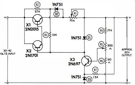
Fig. 6-15. Representative schematic of protective device with instant recovery
feature.

Fig. 6-16. Technique for overvoltage protection of the series losser transistor.
The protective schematic shown in the representative circuit of Fig. 6-15 possesses the operational feature of instant recovery to normal performance when the excessive load is removed. In this circuit current limiting is imposed by the action of zener diode D1 in conjunction with series dropping resistance R1. Resistor R1 is adjusted so that the potential developed across zener diode D1 is insufficient for breakdown under normal load conditions.
However, with excessive load current the increased voltage drop developed across resistance R1 is impressed across D1, causing breakdown of this diode at its rated avalanche voltage. When this occurs, the base of transistor X2 and the collector of transistor X1 become clamped at a voltage considerably negative with respect to the voltage necessary to sustain the condition of current overload. Inasmuch as these are NPN transistors, such action limits current flow in the Darlington pair, X1 and X2. Thus, even a short circuit across the output terminals cannot result in excessive current flow through transistor X1. Some degradation of regulation takes place as a consequence of resistor R1, but this need not be appreciable if it has a low breakdown voltage. This method provides protection against thermal destruction of the series transistor X1. For complete protection of this transistor, it is also necessary to spare it from greater-than-rated collector-emitter voltage. This can be accomplished by appropriate selection of X1 or by also incorporating the protective technique illustrated in Fig. 6-16.
In the event economic, or other considerations preclude the use of a series losser transistor with a collector-emitter voltage rating above the voltage provided by the rectifier filter system, the simple over-voltage protective technique of Fig. 6-16 is recommended. When the regulator is supplying normal load current, the voltage drop across the series losser transistor is insufficient to breakdown the zener diode.
Excessive load current will, however, develop breakdown voltage across this diode. When this occurs, the series losser transistor is protected from voltage higher than that corresponding to the zener breakdown voltage. The zener breakdown voltage should be higher than it would receive during normal operation, but lower than the maximum rated collector-to-emitter voltage of the losser transistor. This technique is most readily applied to low- and medium-power systems. The wattage rating of the zener diode may, in some cases, be sufficient to safely withstand the effects of momentary short circuits. It is more desirable, of course, that this protective diode be able to carry the continuous current of a sustained short circuited output. It is here that difficulties may arise on higher power systems, for a zener diode of very large power handling capacity may be required. (If R1 is included, it must obviously be a compromise value. Too low a value will not protect the zener diode. Too high a value will prevent protection of transistor X1.) This voltage protection method may not give complete protection to the rectifier-filter components. However, in many cases, these may then be protected by a fuse or circuit breaker. This technique can be used in conjunction with other methods of protection. For example, in a high voltage system, the current limiting circuit of Fig. 6-15 should also incorporate a zener diode across the collector-emitter terminals of transistor X1.
The protection of series regulators handling high power or high currents often presents special problems. Energies involved in surges from abrupt changes in current can be considerably more dangerous to components despite the scaling up of ratings over those used at lower power levels.
Additionally, fuses and circuit breakers for high currents generally involve inordinately long actuating times. These matters lead to the design of protective circuitry such as depicted in Fig. 6-17. Here, not only is the connection between rectifier-filter system and the series regulator interrupted, but a moderately heavy artificial load is shunted across the rectifier output. Such a load greatly dampens oscillatory surges. The energy in such surges could endanger components in the rectifier filter system if the protective circuit only interrupted current flow in response to an overload or a short at the regulator output terminals.
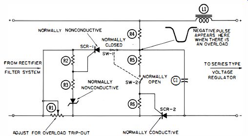
Fig. 6-17. SCR protective circuit diagram.
In Fig. 6-17, the following is true during normal operation : zener diode D1 does not conduct. SCR1 does not conduct. SCR2 does conduct. SW1 is closed. SW2 is open.
(Conduction of SCR2 has been brought about by an initial momentary closure of SW2.) Suppose now, that loading conditions at the output terminals of the regulator cause excessive current consumption. The higher voltage drop thereby developed across resistance R1 causes breakdown of zener diode, D1. This, by virtue of the connection to the j unction of R2 and R3, makes the gate of SCR1 positive with respect to its cathode. As a consequence, SCR1 is turned on and places artificial load R4 across the output of the rectifier-filter system. This, in turn, sends a negative-going pulse through capacitor C1 to the anode of SCR2. Because of this pulse the current flow through SCR2 is momentarily depressed below the value required to maintain conduction. As a result, SCR-2 becomes nonconductive, thereby freeing the series losser transistor from the effects of excessive power dissipation. L1, a small inductance generally in the neighborhood of several tens of millihenrys, aids in the generation of a negative pulse with sufficient energy to reliably turn off SCR2.
Resistor R4 should consume about a third of the maximum rated output current of the system when in normal operation. This allows SCR1 to be a smaller unit than SCR2.
Resistor R1 is adjusted to develop sufficient voltage across zener diode D1 to cause breakdown at some desired overload current. Switches SW1 and SW2 should be spring-loaded to maintain the two switch sections in the contact positions shown except when normally actuated for reset.
Actually, this system is not completely foolproof because its operation is inhibited in the event that this switch is held in its reset position while the output terminals of the regulator are still shorted. A mechanical arrangement whereby SW2 can be momentarily, but not continuously closed would provide considerable safeguard against such a situation. Conversely, this could be accomplished electrically by inserting a small capacitor in the gate lead of SCR2. A discharge path would have to be provided for the capacitor so that the reset function would not be found inoperative due to trapped charge in this capacitor. A resistance in the several megohm range should suffice. (In any event, the resistance must be high enough so that closure of SW2 cannot trigger SCR2 when the small capacitor is removed from the circuit.) Also, the greater the inductance of L1 the more inherent protection is provided against inordinately long closures of SW2 while the regulator feeds a short circuit. This is because L1 slows down the attainment of maximum current flow. Unfortunately, the degree of such protection provided by L1 is limited in practice by the physical size necessary for protection beyond, say several seconds.
For many purposes this general method can be considered to provide very satisfactory protection. This follows from the fact that a condition of overload would normally be analyzed and remedied prior' to reset of the power supply.