AMAZON multi-meters discounts AMAZON oscilloscope discounts
Many types of oscillators are utilized in transistor circuits. In the first analysis, these can be classified as sinusoidal and nonsinusoidal types. For examples, the local oscillator in a TV receiver is a sinusoidal oscillator. On the other hand, the vertical blocking oscillator is a nonsinusoidal oscillator. Sub divisions include free-running and triggered oscillators, mono stable and bistable oscillators, stabilized oscillators, and other subdivisions relating to frequency characteristics. Some oscillators develop continuous-wave signals; others develop amplitude- or frequency-modulated signals. Sweep generators use fm oscillators, for example, to develop frequency-response curves as shown in Fig. 2-1. Let us consider the operating characteristics and waveforms of some basic transistor oscillators.

Fig 2-1. Fm waveform used to develop a frequency response curve.
BLOCKING OSCILLATORS
A transistor blocking oscillator conducts for a short period of time and then is cut off (blocked) for a much longer period of time. A basic circuit for a transistor blocking oscillator using a pnp transistor is shown in Fig. 2-2. If an npn transistor were used in the circuit, the polarities of the collector supply battery V_cc would have to be reversed to maintain reverse bias across the collector-base junction. We will begin our analysis with the instant that the circuit is first energized. Current rises rapidly in the base circuit, due to the forward bias established across the base-emitter junction by the DC power supply V_cc.
Simultaneously, the collector current I_c increases. This increasing collector current induces a negative voltage in the secondary winding of transformer T1.
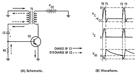
(A) Schematic. (B) Waveform. Fig. 2-2. Transistor blocking oscillator with waveform.
The negative voltage that is induced in the secondary of T1 in Fig. 2-2A is applied at the base of the transistor, and increases the forward bias across the base-emitter junction.
Meanwhile, capacitor C1 charges through the small forward resistance of the base-emitter junction; the transistor is quickly driven into collector saturation, whereupon this rapid regenerative action stops. At saturation, the collector current le becomes constant, and the collector voltage Ve falls to almost zero. Since no more voltage is induced in the secondary winding of T1, C1 stops charging, and starts to discharge through R1. Just before time T1 in Fig. 2B, the magnetic field in the secondary collapses, thereby inducing a voltage of opposite polarity that drives the base of Q1 positive. This reverse bias cuts the transistor off.
Cutoff corresponds to zero base and collector current in Fig. 2-2. At this time, the collector voltage V1 rises and makes the collector more negative than the V1'c supply for a short time following T1. This negative pulse is caused by the same collapse of the magnetic field that drives the base of Q1 positive. The transistor now remains cut off until the stored charge on C1 decays through R1. This occurs at time T2. As soon as there is base current it is amplified by Q1 and fed back re-generatively through T1 to the base. Therefore, Q1 is quickly driven into saturation, and the waveform cycle is repeated.
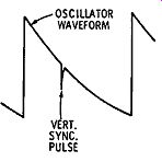
Fig. 2-3. Vertical sync pulse in TV receiver with slowly rolling picture.
Next, let us consider how the blocking oscillator in Fig. 2-2 can be synchronized. If negative-going sync pulses are coupled into the base circuit, they will ride on the V 81 waveform, and will extend downward toward the 0-volt level. It is evident that as a negative-going sync pulse approaches the 0-volt level in the time interval from T1 to T2, Q1 will be triggered into conduction somewhat sooner than if the sync pulse were absent. (See Fig. 2-3). Therefore, the blocking oscillator can be locked in frequency by the sync pulse. In normal operation, we adjust the value of R1 so that the oscillator runs a little slower than the repetition rate of the sync pulses. Accordingly, the incoming sync pulses speed up the repetition rate of the oscillator, compared with its free-running frequency.
Next, let us consider the free-running frequency of the blocking oscillator shown in Fig. 2-2. A capacitor charges and discharges through resistance according to an exponential waveform, as shown in Fig. 2-4. We measure charge and discharge intervals in time constants. One time constant is equal to the product, in seconds, of the capacitance and the resistance.
T == RC (2.1)
where,
T denotes the time constant of the RC circuit in seconds, R denotes the resistance in ohms, C denotes the capacitance in farads.
Observe in Fig. 2-4 that a capacitor discharges to 37 percent of its initial voltage in one time constant. At the end of four or five time constants, the capacitor charge has decayed to nearly zero. Therefore, the free-running blocking oscillator in Fig. 2-2 has a repetition rate that is equal to approximately four or five time constants. Its exact repetition rate depends on the particular transistor, and how close its base voltage must approach zero to start a base-current. Next, with respect to the charging interval of C1, we recognize that as soon as there is base current, R1 is shunted by the low value of base-emitter resistance in Q1. This base-emitter resistance has a very low value, in the order of 35 ohms. Therefore, the charging time constant is very short, and can be charged very rapidly.
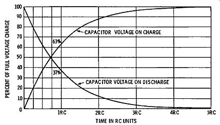
Fig. 2-4. Universal RC time-constant chart.
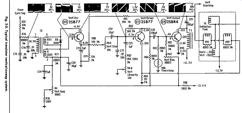
Fig. 2-5.
The exponential waveform chart shown in Fig. 2-4 is basic in analysis of nonsinusoidal oscillators. In other words, a blocking oscillator is basically an exponential waveform generator, as seen in the V B1 waveform of Fig. 2-2B. Therefore, it would be impractical to analyze the operation of the circuit on the basis of sine waves. To understand the circuit action, we must use exponential waveforms as our basic reference. Of course, the V B1 waveform in Fig. 2-2B is not a pure exponential; it begins and ends with pulses. That is, the base waveform is a combination exponential and pulse waveform. Combination waveforms are the rule, rather than the exception in transistor circuits.
Let us now compare the waveforms for transistor Q14 in Fig. 2-5 with the V B1 and V c waveforms in Fig. 2-2B. At first glance, the waveforms seem to be different. However, the difference is chiefly in the scaling, rather than the waveshapes. Be- cause of the additional circuit components, the base waveform of transistor Q14 has a large pulse component, and a less steeply sloping exponential component. Although there are superficial differences, the basic waveform is the same as that of VB1. The collector waveform for Q14 is also basically similar to that of V c, However, the positive peak of the waveform for Q14 is modified somewhat, due chiefly to the presence of diode XS. Diodes are used in blocking-oscillator circuits to limit the peak voltage that is applied to the transistor by the collector waveform, and also to clip the sync pulses for stable triggering action. With reference to Fig. 2-6, resistor R5, in series with R4, operates as a damping control to set the amplitude of the output positive pulse. Diode X2 is connected across the primary of T1 to protect the transistor. That is, the collapsing magnetic field of T1 might exceed the breakdown voltage of the transistor used in the circuit. However, X2 is driven into forward conduction as the magnetic field collapses, and thereby limits the pulse amplitude across the primary. Additional reduction of amplitude can be obtained by adjustment of R5.
cause of the additional circuit components, the base waveform of transistor Q14 has a large pulse component, and a less steeply sloping exponential component. Although there are superficial differences, the basic waveform is the same as that of VB1. The collector waveform for Q14 is also basically similar to that of V c, However, the positive peak of the waveform for Q14 is modified somewhat, due chiefly to the presence of diode XS. Diodes are used in blocking-oscillator circuits to limit the peak voltage that is applied to the transistor by the collector waveform, and also to clip the sync pulses for stable triggering action. With reference to Fig. 2-6, resistor R5, in series with R4, operates as a damping control to set the amplitude of the output positive pulse. Diode X2 is connected across the primary of T1 to protect the transistor. That is, the collapsing magnetic field of T1 might exceed the breakdown voltage of the transistor used in the circuit. However, X2 is driven into forward conduction as the magnetic field collapses, and thereby limits the pulse amplitude across the primary. Additional reduction of amplitude can be obtained by adjustment of R5.
Resistor R3 serves two functions in this circuit. First, it provides emitter bias due to emitter current. As a transistor heats up, the emitter current tends to increase. If this tendency were not counteracted, the repetition rate would change. Since increased emitter current produces greater bias voltage across

Fig. 2-6. Synchronized transistor blocking oscillator.
Resistor R3 serves two functions in this circuit. First, it provides emitter bias due to emitter current. As a transistor heats up, the emitter current tends to increase. If this tendency were not counteracted, the repetition rate would change. Since increased emitter current produces greater bias voltage across R3, the oscillator is self-stabilizing. Secondly, a pulse output signal can be taken from across R3. We often find a capacitor C4 used to bypass the emitter resistor. Since the capacitor tends to hold its charge between pulses, it improves stabilizing action. An emitter bypass capacitor also decreases the free running frequency of the blocking oscillator, although this circuit action is merely incidental.
If C4 in Fig. 2-6 is chosen in a suitable value so that R3 is partially bypassed, another useful function can be served. That is, the capacitor partially discharges between pulses, with the result that an exponential waveform is produced by the emitter in accordance with the discharge waveform depicted in Fig. 2-4. Thereby, the emitter circuit operates as a waveshaping circuit, and produces a semi-sawtooth wave. Of course, this is not a true sawtooth waveform because it has an exponential curvature. However, additional waveshaping circuitry can be used to obtain a true sawtooth waveform.
The free-running frequency of the blocking oscillator in Fig. 2-6 is determined chiefly by capacitors C2 and C3, and resistors R1 and R2. That is, these capacitors and resistors have a certain time constant that determines when Q1 will come out of cutoff. Note also that R1 is not returned to ground as in Fig. 2-2, but, instead, to the voltage source Vee- The reason for this connection is that V f'<' causes Q1 to come to output cutoff earlier than if R1 were grounded. In turn, the exponential waveform at the base is not so greatly curved, and the trigger point is less affected by random noise voltages that might gain entry to the circuit.
Sync pulses are capacitively coupled to the base of Q1 in Fig. 2-6. Negative-going sync pulses are used, as previously explained. It is undesirable to have any positive noise pulses, or positive excursions of sync pulse applied to the base, because they would affect the time constant of the discharge circuit.
Therefore, diode X1 is connected between base and emitter of Q1 to short-circuit any positive excursions that might be coupled into the oscillator circuit. Control R1 is adjusted to make the free-running frequency of the oscillator slightly lower than that of the incoming sync pulses. Output waveforms may be taken either from the tertiary winding on T1, or from the emitter of Q1, or both.
TRANSISTOR MULTIVIBRATORS
Transistor multivibrators are widely used in electronics technology. For example, many thousand multivibrators may be included in an electronic computer system. The free-running (astable) multivibrator is basically a two-stage amplifier with its output fed back to its input. RC circuitry is employed that has uniform response out to high frequencies. In turn, complex waveforms related to the basic square wave are produced.
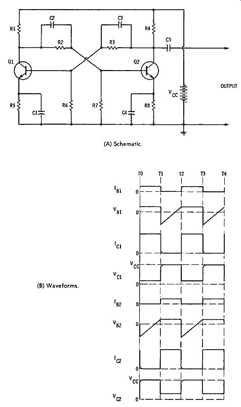
Fig. 2-7 A shows a typical configuration for an astable transistor multivibrator.
While one stage conducts, the other stage is cut off. At a certain point that
depends on RC time constants, the stages reverse their conditions-the conducting
stage suddenly cuts off, while the nonconducting stage suddenly starts to conduct.
Thus, a form of square wave is generated. The emitter-coupled transistor multivibrator
configuration employs feedback via its common-emitter resistor. On the other
hand, a collector-coupled multivibrator employs coupling capacitors as shown
in Fig. 2-7 A. The waveforms for the collector-coupled multivibrator arrangement
are shown in Fig. 2-7B. The circuit comprises a two-stage, RC-coupled, common-emitter
amplifier that uses npn transistors in this example. If pnp transistors were
used, the collector supply battery V cc would be reversed in polarity.
Output from the first stage is coupled to the input of the second stage; also, output from the second stage is coupled to the input of the first stage. We recall that there is a 180-degree phase shift (polarity reversal) between the input and output of a CE configuration. This means that the output of each stage is in phase with the input to the other stage. Regenerative feed back provides the signals required for sustained oscillation.
Let us assume in Fig. 2-7 A that Q1 conducts more heavily than Q2 when operating voltages are applied. From time T0 to time T1 in Fig. 2-7B, collector current Ici and collector voltage Vn remain constant; capacitor C2 discharges through resistor R7 in accordance with the exponential waveform depicted in Fig. 2-4. As C2 discharges through R7, the voltage drop across R7, which is also the base voltage of Q2 (V n2), decreases; this effectively decreases the reverse bias on Q2. This action continues until time T1, whereupon forward bias is re-established across the emitter-base junction of Q2, and Q2 starts to conduct.
As the collector current I('~ through Q2 increases, collector voltage V c~ becomes less positive from T1 to T2. This voltage, coupled through capacitor C3 to the base of Q1, drives the base more negative and causes a decrease in collector current lei through Q1.

Fig. 2-7. Transistor multivibrator. (A) Schematic. (B) Waveforms.
Increased positive voltage at the collector of Q1 in Fig. 2-7 A is coupled through C2 and appears across R7. Collector current It·~ through Q2 therefore increases. This process continues rapidly until Q1 is cut off. Transistor Q1 remains cut off and transistor Q2 conducts until C3 discharges sufficiently through R6 to decrease the reverse bias Vm on the base of Q1 so that the operating cycle repeats following time T2. When checking waveforms with a scope, beginners are sometimes confused by the aspect of a waveform. That is, if the scope controls are varied, a square wave may appear in different scaling, as demonstrated by Fig. 2-8. Note that the second aspect is not a pulse, but is still a square wave, because the duty cycle is equal to 1.
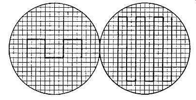
Fig. 2-8. Two aspects of square wave.

Fig. 2-9.
Resistors R1 and R4 in Fig. 2-7A are the collector load resistors for Q1 and Q2, respectively. Suitable bias for the base of Q1 is provided by a voltage-divider network comprising R3 and R6. Base bias voltage for Q2 is provided by R2 and R7.
Resistors R5 and RS are temperature stabilization resistors for Q1 and Q2. C1 and C4 are emitter bypass capacitors. The repetition rate of the multivibrator depends on the time constants of the RC-coupling networks, modified by the bias voltages which determine the point on the exponential decay curve that a transistor comes out of cutoff. The output signal is coupled through capacitor C5 to the load. The signal is basically a square wave, although it must be passed through a subsequent waveshaping circuit to obtain a good approximation to an ideal square wave. Output could also be taken from the collector of Q1. Electronic switches are designed around astable multivibrators. A typical configuration is shown in Fig. 2-9. The multivibrator transistors are QS and Q9. Three repetition rates can be obtained by setting SI to switch different values of coupling capacitors into the circuit. Amplifiers A and B pass input signal alternately because the square wave causes Q5 and Q6 to con duct alternately. To obtain good switching action the output from the multivibrator is passed through the waveshaper comprising Q10 and Q1l. In addition, the rise time of the square wave is improved. Signals at input A and input B are switched alternately into Q7, which operates in the common-emitter con figuration and provides isolation between the mixer section and the scope input circuit. Details of waveshaping circuits are discussed subsequently.
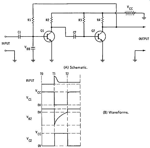
Fig. 2-10. Transistor one-shot (monostable) multi vibrator. (A) Schematic.
(B) Waveforms.
Another important type of multivibrator is called the mono stable, one-shot, single-shot, or single-swing configuration, as shown in Fig. 2-10A. When this configuration is triggered, it goes through a complete cycle of operation, and then returns to its original quiescent state. An external trigger pulse moves the operating point from the initial stable region. The time constant of the RC components holds the operating point in its new stable region for a determined period of time. Then, the operating point moves back into the original stable region.
When in its initial stable region, or quiescent condition, transistor Q2 is in saturation and Q1 is cut off. A positive trigger pulse of short duration applied to the base of Q1 causes the multivibrator to go through its active cycle. Then, the circuit rests in its quiescent condition until another trigger pulse arrives.
Battery V<'c supplies the necessary collector voltages for the transistors in Fig. 2-10A, and also supplies the forward bias for the emitter-base junction of Q2. Transistor Q2 is in saturation during the quiescent period; therefore, the collector voltage is practically zero. Fig. 2- 10B shows the collector wave form V ('~ during this time from TO to T1. Reverse bias across the emitter-base junction provided by battery V('(' maintains Q1 at cutoff. Collector voltage V('J is positive and equal to battery voltage v, .... The collector waveform Cn during this same time is shown in Fig. 2- 10B. Capacitor C2 is charged to the value of battery voltage v,.,, through the essentially short-circuited base-emitter junction of forward-biased Q2 and the collector load resistor R2.
If a positive input trigger pulse is applied at time T1 to the base of Q1 via C1, Q1 is driven into conduction. Collector voltage V.,1 at time T1 decreases, or becomes less positive. C2 immediately starts to discharge through R3. Regenerative signal action from the collector of Q1 occurs via C2 to the base of Q2.
A maximum negative voltage v11 ~ is applied to the base of Q2 at time T1. This places reverse bias across the emitter7base junction, and drives Q2 toward cutoff. As collector current through Q2 decreases, the collector voltage rises. This rise is coupled via R1 to the base of Q1, and increases its positive voltage. This regenerative action causes a rapid change of state in both transistors. It drives Q1 toward saturation and drives Q2 toward cutoff. When collector current ceases to flow at time T1, Tc~ rises to equal V re, From time T1 to T2 in Fig. 2-10B, C2 is discharging via R3 and the low saturation resistance of Q1. Capacitor C2 reaches 0 volts at T2, and Q2 then has the necessary reverse bias to keep the collector current cut off. Hence, at time T2, collector current starts to rise, drives Q2 into saturation, and brings V,•~ to 0 volts. At this time, regenerative voltage from the collector of Q2 is coupled to the base of Q1 through R1 and falls to 0 volts, and V,.., once again provides reverse bias driving Q2 back into cutoff.
The collector voltage V ci in Fig. 2-10 again equals V cc at time T2, and capacitor C2 recharges through the emitter-base junction of Q2 and resistor R2. C2 continues to charge up to the collector supply voltage, when further circuit action ceases.
If another trigger pulse is applied at the base of Q1, another cycle of operation ensues. Output is taken from the collector of transistor Q2. The collector waveform V c2 is basically a square wave, although its rise time can be improved by processing the waveform through suitable waveshaping circuitry. The duration of the output pulse from T1 to T2 is primarily determined by the time constant of R3 and C2 during discharge. Of course, the repetition rate of the output waveform is determined by the input trigger pulses.
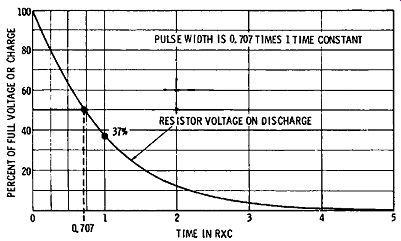
Fig. 2-11. Pulse width measurement.
Waveform VB2 in Fig. 2- 10B is a semi-sawtooth, and may also be regarded as a pulse waveform. Its decay is essentially exponential. We measure pulse width between the 50 percent of maximum points on the leading and trailing edges, as indicated in Fig. 2-11. Waveform VB2 is usually called a pulse be cause it is not immediately followed by another cycle. In other words, a pulse is a waveform that occurs at separated time intervals. On the other hand, if the same waveform is immediately followed by another excursion, it is usually called a semi sawtooth waveform. Fig. 2-12 illustrates sawtooth waveforms that have the same amplitude, but different frequencies, and sawtooth waveforms that have the same frequency, but different amplitudes.
(A) Sawtooth waveforms with same amplitude.
(B) Sawtooth waveforms with same frequency.
Courtesy Allied Radio Corp.

Fig. 2-12. Distinction between amplitude and frequency.
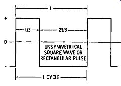
Fig. 2-13. Rectangular waveform.
Basically, frequency and repetition rate have the same meaning. However, we usually speak of the frequency of sine waves and the repetition rate of complex waves. Frequency is measured in hertz, and repetition rate can also be denoted in hertz. However, it is customary to speak of repetition rates in terms of pulses per second (pps). The term "pulses" in this connotation is very broad, and applies to almost any complex waveform. We will find that the distinction between pulses and square waves, for example, is not sharply drawn. Fig. 2-13 depicts a waveform that is called an unsymmetrical square wave, or a rectangular pulse. If the RC time constants are made unequal in Fig. 2-7 A, the output waveform is not a square wave, but a rectangular waveform.
Exponential pulses are related to square waves as shown in Fig. 2-14. The voltage drop across the resistor is an exponential pulse, and is called a differentiated square wave. The complex waveform that is dropped across the capacitor is called an integrated waveform. These terms follow from mathematical analyses that are beyond the limits of our format. The RC circuit obeys Kirchhoff's voltage law:
E1 = E2 + E3 (2.2)
The lower diagram in Fig. 2-14 shows how the addition of waveforms E2 and E3 results in a sum equal to waveform E1.
In this example, the time constant of the RC circuit is sufficiently short with respect to the repetition rate of the square-wave input that E2 falls practically to zero before the next excursion starts. The peak-to-peak voltage of E2 is practically double the peak-to-peak voltage of E1 ; E:i has the same peak to-peak voltage as E1
With reference to Fig. 2-4, we recognize that waveform Ea has the same basic curvature as waveform E2 "turned upside down." This fact follows from Formula (2.2).
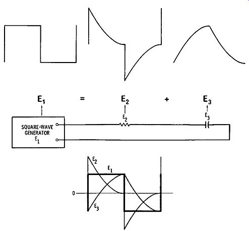
Fig. 2-14. Kirchhoff's voltage law applied to square-wave response of RC circuit.
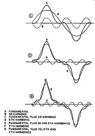
Fig. 2-15. Build-up of positive pulse followed by negative pulse.
Pulses can be synthesized, or built up, from sine waves, just as in the case of square waves. Fig. 2-15 depicts the build-up of a symmetrical ac pulse from a fundamental and its harmonics. Of course, a very large number of harmonics must be included to obtain a pulse waveform that has smooth leading and trailing edges. We will find that the harmonic frequencies in waveforms E2 and E3 in Fig. 2-14 are the same as the harmonic frequencies in a square wave. This is necessarily so because the square-wave harmonics flow into the RC circuit, and none of these harmonics are removed; neither are other harmonics added or generated by the linear RC circuit. There-fore, the only distinction between the harmonics in E1 and in E~ or E:i consists in their comparative amplitudes. That is, the capacitor has decreased reactance for the higher harmonic frequencies and passes these frequencies at comparatively high amplitude.
This is just another way of saying that the drop across the resistor in Fig. 2-14 is a waveform that has harmonics with large amplitudes, compared to the input square wave-the capacitor reduces the amplitude of the fundamental current, and also the amplitudes of the lower harmonic currents. There fore, the differentiated waveform contains comparatively large-amplitude harmonics. The opposite condition is found across the capacitor-the fundamental and low harmonic frequencies produce a comparatively large voltage drop across the capacitor.
The effect of varying the time constant of an RC circuit on the differentiated and integrated waveforms for an applied square wave is shown in Fig. 2-16. An RC coupling circuit is the same as a differentiating circuit except that it has a very long time constant-in excess of 5RC. Therefore, a coupling circuit does not noticeably differentiate a square wave. Fig. 2-16 also shows the effects of differentiation and integration of an applied sawtooth waveform, when the RC circuit has various time constants. When the time constant is in excess of 5RC, we can regard the configuration as a coupling circuit.
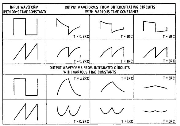
Fig. 2-16. Square-wave and sawtooth reproduction in series RC circuits with
differing time constants.
QUIZ
1. Name two basic classifications of transistor oscillators.
2. Define a blocking oscillator.
3. Describe the general nature of the waveforms produced in a blocking-oscillator circuit.
4. What determines the polarity chosen for a sync pulse in a blocking oscillator?
5. Explain the units of time used in a universal RC time-constant chart.
6. How much does an exponential waveform decay in one time constant?
7. Discuss the function of diodes utilized in a blocking-oscillator circuit.
8. Define a free-running (astable) multivibrator.
9. Describe the general nature of the waveforms produced in a multivibrator circuit.
10. Explain what is meant by the aspect of a square wave.
11. How does an electronic switch operate?
12. Define a one-shot multivibrator.
13. Describe the general nature of the waveforms produced in a one-shot multivibrator circuit.
14. How is pulse width measured?
15. Distinguish between a semi-square wave and an ideal square wave.
16. How can the shape of a semi-square wave be improved?
17. Explain the distinction between symmetrical and unsymmetrical square waves.
18. Describe the application of Kirchhoff's voltage law to a series RC circuit that is energized by a square wave.
19. How are the harmonics in a differentiated pulse related to the harmonics of a square wave?
20. Distinguish between a differentiating circuit and an RC coupling circuit.
21. How does the time constant of a differentiating circuit affect the output waveform?
22. Describe the effects of differentiation and integration on a sawtooth waveform.
23. Why is an exponential waveform sometimes called a semi sawtooth waveform?
24. Describe a frequency-modulated wave.
25. State an application for a frequency-modulated waveform.