AMAZON multi-meters discounts AMAZON oscilloscope discounts
The distinction between oscillators and waveshapers is not sharply drawn. For example, a one-shot multivibrator is often called a monostable oscillator; it is also called a pulse regenerator. A pulse regenerator is used to produce a standard pulse waveform. For example, in an electronic computer, a pulse must pass through many circuits; as it progresses through various circuits, the pulse waveform becomes distorted. Since excessive distortion can result in erratic operation, a pulse that has undergone a certain amount of distortion may be fed to a one-shot multivibrator that restores the standard pulse shape and width. In this application, the one-shot multivibrator operates solely as a waveshaper. That is, whether we regard a con figuration as an oscillator or as a waveshaper depends on its application.
Thus, the bistable (Eccles-Jordan) multivibrator shown in Fig. 3-1 may be regarded either as an oscillator or as a wave shaper. When bistable multivibrators are connected in cascade, they function as memory systems in electronic computers (see Fig. 3-2) ; in this application the bistable multivibrator is called a flip-flop (FF). If neon bulbs or other visual indicators are connected into the cascade circuit, binary readout of stored numbers is provided. Details on this are reserved for subsequent discussion. As a waveshaper, a bistable multivibrator may be triggered by the output from an audio oscillator. In turn, a square-wave output is provided that has the same repetition rate as that of the audio oscillator.
Let us consider the circuit action of the bistable multivibrator in Fig. 3-1A. It differs from a one-shot multivibrator primarily in that it requires two input triggers to complete one cycle of output. A flip-flop is in a stable state when either transistor is conducting while the other transistor is cut off.
The transistor states are switched by application of a trigger pulse. When DC power is first applied, one transistor conducts, whereas the other transistor is cut off. The conducting transistor quickly saturates; the collector current of the other transistor is practically zero. Each transistor remains in this stable state each being steadily biased by the other, until a trigger pulse is applied. A negative pulse applied to the base of a pnp transistor in its conducting state has no switching action. In other words, the transistor is already conducting.
On the other hand, the same negative trigger pulse applied to the base of the cut-off pnp transistor will change the state of the circuit.

Fig. 3-1. Transistor Eccles-Jordan multivibrator.
Courtesy Computer Control Co., Inc. (A) Schematic. (B) Waveforms.
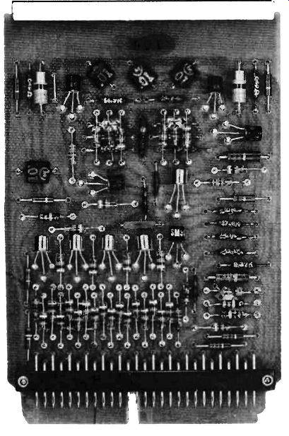
Fig. 3-2. Transistor module for digital computer.
The transistor that was cut off is driven briefly into conduction by the trigger pulse and feedback causes the other transistor to be driven into cutoff. Thus, the states are reversed, and the transistors remain in this stable state, each being steadily biased by the other. Note that a positive trigger pulse applied to the base of the conducting transistor will also change the state of the circuit. Basically, the method used to trigger an FF is determined by the polarity and magnitude of the available trigger pulse, and the desired repetition rate of the output waveform. Although the FF depicted in Fig. 3-lA uses a trigger pulse applied to the bases of both transistors, a trigger pulse of sufficient amplitude and proper polarity could also be applied to the collector of either transistor.
Let us assume that Q1 is conducting and Q2 is cut off in Fig. 3-lA. A negative trigger pulse applied to the base of each transistor at time TO in Fig. 3-1B causes Q2 to conduct. The in creasing collector current causes the collector voltage v"~ of Q2 to decrease (become less negative). This voltage change is coupled to the base of Q1, and reduces its forward bias. Col lector current through Q1 begins to decrease, and collector voltage V c1 changes from zero to a negative value that approaches the battery voltage V cc- This voltage change is coupled to the base of Q2, making the base more negative, and increasing the conduction of the transistor. Regenerative feed back continues until Q2 is saturated and Q1 is cut off.
Transistor Q2 in Fig. 3-1A continues conducting, and Q1 remains cut off. The transistors remain in this state until the next trigger pulse is applied at time T1; then Q1 conducts and Q2 is cut off. This completes one full cycle of the output square wave. The time constant of C1 and R2 and C2 and R6 basically determines the time from conduction to cutoff of Q1 and Q2.
The capacitors provide rapid coupling of voltage changes, and the switching action is therefore rapid. The output waveform is coupled via C5 to the load. Note that output could be taken from Q2. Since an FF requires two input triggers to produce a complete output cycle, it operates as a frequency divider with a ratio of 2 to 1.

Fig. 3-3. Push-pull square-wave outputs.
Resistors R1 and R5 in Fig. 3-1A provide the DC collector loads for the transistors. The necessary forward bias for Q1 and Q2 is provided by a voltage-divider network comprising R3 and R6 for Q1, and R7 and R2 for Q2. R4 provides emitter temperature stabilization, and provides operating stability. C3 and C4 couple the input trigger pulse to the base of each transistor. Note that if outputs are taken from both Q1 and Q2, we obtain a push-pull output, as shown in Fig. 3-3. The rise time of the output waveform depends on the ratio of collector load resistance to the stray capacitance in the load circuit.
Therefore, faster rise time can be obtained by using low values of collector load resistance. However, the output amplitude tends to decrease with low values of collector load resistance because the transistor's internal resistance is not zero during collector saturation.
When a transistor is saturated, its internal resistance may be in the order of 35 ohms. If a 2,000-ohm collector-load resistance is used, the collector voltage drops to nearly zero during saturation. On the other hand, if we use a 75-ohm collector-load resistance, the collector voltage will be about one third of the supply voltage during saturation. In either case, the collector voltage will be practically equal to the supply voltage when the transistor is cut off, because its internal resistance is very high in this state.

Fig. 3-4. Effect of differentiation on square wave.
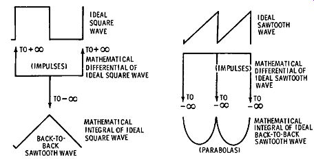
Fig. 3-5. True differentials and integrals of ideal square and sawtooth waveforms.
RC CIRCUIT DIFFERENTIATION VERSUS MATHEMATICAL DIFFERENTIATION
Consider the case in which C5 in Fig. 3-1A feeds into a comparatively low value of resistance. Then, the square-wave output becomes differentiated into a narrow exponential pulse, as depicted in Fig. 3-4. If a very short time constant is used, the pulse becomes very narrow, and approaches an impulse.
An impulse has zero width, as shown in Fig. 3-5, and represents the mathematical differentiation of a square wave. If an ideal square wave is applied to an ideal integrator, an output waveform is obtained that is called a back-to-back sawtooth wave. An approximate back-to-back sawtooth wave is obtained by RC integration of a square waveform.
Note in Fig. 3-5 that ideal differentiation of a sawtooth waveform produces an impulse waveform. Ideal integration of an ideal back-to-back sawtooth wave produces a parabolic waveform. In color-TV receivers, sawtooth waveforms are integrated by RC circuits to produce approximate parabolic waveforms. This circuit action is employed in convergence circuitry. We know that when a square wave is differentiated, the fundamental and low-frequency harmonics are reduced in amplitude, compared with the high-frequency harmonics.
Therefore, the harmonics are stronger in a pulse than in a square wave. Fig. 3-6 shows the comparative harmonic amplitudes for a square wave and a rectangular pulse. The narrower the pulse, the stronger the comparative amplitudes of the high-frequency harmonics.
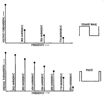
Fig. 3-6. Harmonic content of square waves and pulses.
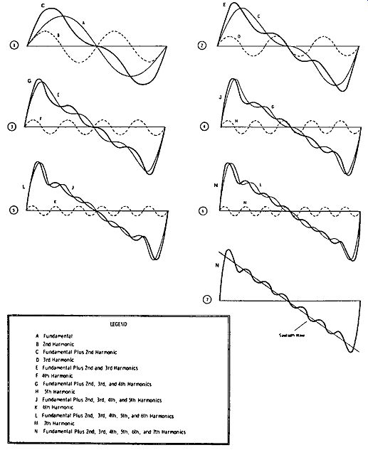
Fig. 3-7. Composition of sawtooth waveform.
In an impulse wave, we have a theoretical limiting situation in which the pulse width is zero, the pulse amplitude is infinite, and all the harmonics in the impulse have the same amplitude as the fundamental. Of course, a true impulse waveform can not be produced in practice, although exponential pulses that approach an impulse waveform can be produced by using a differentiating circuit with a very short time constant. With reference to the ideal sawtooth waveform in Fig. 3-5, we note that a sawtooth waveform can be synthesized or built up from sine waves, as shown in Fig. 3-7. Mathematically speaking, this synthesis represents the Fourier series for a sawtooth wave form. Although useful conclusions can be drawn from the synthesis viewpoint, we must be on guard to avoid misapplication of this concept. For example, if an ideal sawtooth waveform is integrated, the higher-frequency harmonics are removed. In turn, we might expect the output waveform to be "wavy"; however, the integrated output is a smoothly curved waveform.
Let us see· why misapplication of the synthesis concept leads us to a false conclusion in the foregoing example. If an ideal sawtooth waveform were to be built up from sine waves, as depicted in Fig. 3-7, an infinite number of harmonics would be required. This corresponds to a circuit that has infinite band width. In practice, however, we know that it is impossible for a circuit to have infinite bandwidth. Therefore, conclusions drawn from the synthesis concept may be in error. In an RC integrating circuit, exact analysis requires that we abandon the synthesis concept, and describe the circuit action on the basis of exponential waveforms. An ideal exponential wave form can exist in a circuit that has limited bandwidth. On the other hand, an infinite number of harmonics cannot exist in a circuit that has limited bandwidth.
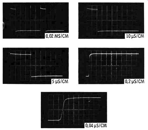
Fig. 3-8. Expansion of 20-microsecond pulse with increasing sweep speed.
EXPANSION OF RECTANGULAR WAVEFORMS
Although the output from a square-wave or pulse generator, or from the circuit in Fig. 3-1, might seem to have straight lines, sharp corners, and vertical sides, it is easy to show that such waveforms are actually combinations of various exponential waveforms. For example, if we expand any pulse wave form on the screen of a triggered-sweep scope, we observe the development illustrated in Fig. 3-8. At high sweep speeds, it becomes evident that the corners are not sharp, but instead are rounded; the leading edge of the waveform is not vertical, it slopes-the pulse has a certain rise time. In summary, the waveform actually consists of a certain combination of exponential waveforms.
A square wave or pulse produced by a generator has a certain rise time; a scope also has a certain rise time. If the rise time of the scope is very fast, compared to the rise time of the generator, we regard the rise time displayed on the scope screen as the rise time of the generator. On the other hand, if the rise time of the generator is very fast, compared with the rise time of the scope, we regard the rise time displayed on the scope screen as the rise time of the scope. Again, when the rise times of the generator and of the scope are in the same order of magnitude, the rise time displayed on the scope screen depends on both the generator rise time and the scope rise time.
It can be shown that the rise time in this situation is formulated:
Rise Time= v T12+ T22 (3.1)
... where, T 2 denotes the rise time of the scope's vertical amplifier, and T1 denotes the rise time of the generator.

Fig. 3-9. How rise times combine.

Fig. 3-10. Distortions commonly observed in square and pulse waveforms.
Fig. 3-9 illustrates the meaning of Formula (3.1). The rise time of the input square wave is T1 ; the rise time of the scope's vertical amplifier is T2.
In turn, the displayed waveform has a slower rise time that is given by Formula (3.1). Practical square waves and pulses often have various distortions, as depicted in Fig. 3-10. We may observe preshoot, overshoot, ringing, tilt, and corner rounding. In measuring rise time, pre swing and/or overshoot are disregarded in locating the 10-percent and 90-percent points on the leading edge. That is, we assign a zero value to the base line, and a 100-percent value to the flat top. For example, consider the points depicted in Fig. 3-11; the flat top is preceded by overshoot and ringing. We regard the flat top as the 100-percent level, and locate the 10 percent and 90-percent points accordingly for measurement of rise time.
Let us briefly consider the circuit actions that produce the distortions pictured in Fig. 3-10. Pre-swing is not observed in simple circuits; however, it can be produced in delay lines, and also in certain types of video amplifiers, such as used in color TV receivers. Corner rounding occurs because all circuits have residual inductance and capacitance, which prevent current from flowing instantaneously when a voltage is suddenly applied. Therefore, a small elapsed time is required for the circuit to change from its resting state and to enter the rise interval of the waveform. The relation of rise time to bandwidth was given in Formula (1.1), which we repeat here:
1 T. = 3fc (3.2)
Note that Formula (3.2) is not absolutely exact, but is sufficiently accurate for practical work. Overshoot is caused by leakage inductance and stray capacitance in a circuit or amplifier. That is, the leakage inductance of peaking coils in a video amplifier can be tuned by shunt stray capacitance to form a resonant circuit that "rings" when a square wave or pulse is applied. The first half-cycle of the ringing waveform appears as overshoot in the reproduced square-wave or pulse pattern. Subsequent excursions appear as a ringing interval that has the form of a damped sine wave. This means that the sine wave decays exponentially. Tilt is produced by a small amount of differentiation through RC-coupling circuit. Under shoot and ringing following the trailing edge of a waveform are produced by leakage inductance and stray capacitance.
Preshoot or undershoot, and overshoot are sometimes en countered also in transistor waveshaping circuits. In such a case, the "pips" result from a strong drive waveform applied to an RC-coupling circuit; the coupling circuit is associated with a semiconductor device that starts to differentiate the applied drive waveform, and then quickly settles down to a "flat top" response. In turn, the differentiated "pip" appears in the output waveform as an overshoot, undershoot, or pre shoot, depending on the circuit configuration. Well-designed waveshaping circuits are free from "pips" in the output wave form. The damping time of a ringing waveform is measured as shown in Fig. 3-12. Damping time is measured in micro seconds or milliseconds with a triggered-sweep scope that has calibrated sweeps.
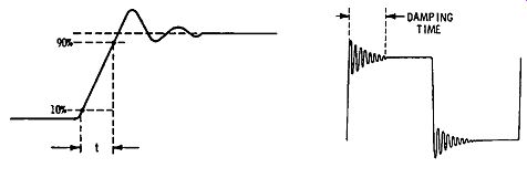
Fig. 3-11. Measurement of rise time t.

Fig. 3-12. Damping time of ringing waveform.
(A) Schematic. (B) Waveforms.
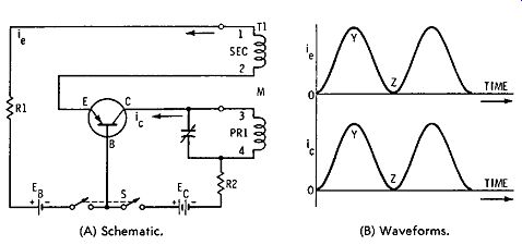
Fig. 3-13. Tickler feedback oscillator.
SINUSOIDAL TRANSISTOR OSCILLATORS
Sinusoidal transistor oscillators normally generate output waveforms that approach a sine waveshape. A well-designed oscillator of this type generates an almost ideal sine wave. A pnp transistor oscillator using a tickler coil for inductive feed back is shown in Fig. 3-13. The base is common to the input and output circuits. E8 biases the emitter-base input circuit for forward-current flow. Vr biases the collector-base junction in the reverse direction. Waveforms of emitter current h: and collector current ic are shown in Fig. 3-13B. Oscillation starts when switch S is closed. Emitter current h:, and collector current ic, both increase from O to Y, because of regenerative feedback in T1 from the 3-4 winding to the 1-2 winding.
At point Y in Fig. 3-13B, the transistor is saturated and no further increase in current flow can occur. Therefore, feed-back ceases and iE starts to decrease. In turn, collector current ic starts to decrease. Feedback via T1 reverses the signal polarity and causes iE to decrease to zero. At point Z, feedback again ceases. When the feedback voltage has driven the transistor to cutoff, the bias voltages return to their original values, and the oscillation cycle is repeated. The time between cutoff and saturation of the transistor is determined chiefly by the resonant frequency of the tank circuit. The frequency of the generated sine wave is stated approximately by the familiar resonant-frequency formula:
f = 2 pi ~ (3.3)
The higher the Q value of the tank circuit, the more nearly does the oscillating frequency approach the value given by Formula (3.3). Also, the higher the Q value of the tank, the more nearly does the output waveform approach a true sine wave shape. If the Q value is quite low, the output waveform will be a badly distorted sine wave. The Q value of the tank circuit is formulated: where, XL is the inductive reactance of the tank coil, and R is its effective series resistance.
Inductive reactance, we recall, is formulated: XL= 2 pi fL where, XL denotes reactance in ohms, f denotes frequency in hertz, and L denotes inductance in henrys.
(3.4)
(3.5)
Note that the effective resistance of L is not simply its winding resistance. That is, the coil has a high-frequency (rf) resistance that is greater than its DC resistance. Moreover, the effective resistance of the tank coil is increased by the shunt resistance of the transistor and the resistance that is coupled into the tank coil by the tickler coil. Therefore, calculation of the effective resistance of the tank coil is comparatively difficult, and is not developed in detail here.
In Fig. 3-14, an npn transistor is employed in a Hartley oscillator circuit. The tapped coil is returned to the common emitter point. The collector circuit may be either shunt-fed, as in Fig. 3-14A, or series-fed, as in Fig. 3-14B. Resistor Rn limits the base-emitter bias current to a suitable value. L and C values of the tank circuit determine the frequency of oscillation. C_B prevents the tank coil from short-circuiting the base-emitter junction of the transistor. R,: limits the collector current to a safe value, and CE eliminates negative feedback. V11 provides bias current for the input, and collector voltage for the output circuit.
(A) Shunt-fed collector. (B) Series-fed collector.
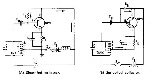
Fig. 3-14. Npn junction-transistor Hartley oscillator.
(A) Schematic. (B) Waveforms.

Fig. 3-15. Colpitts transistor oscillator.
We observe that the tapped tank coil produces regenerative feedback in the same basic manner as a tickler coil. The oscillation frequency is somewhat lower than the value given by Formula (3.3) because of the loading that the transistor imposes on the tank circuit. If the Q value of the tank circuit is high, the output waveform approximates a true sine wave. On the other hand, low Q values are associated with a distorted sinewave output. It is also necessary to locate the tap point on the tank coil properly, to obtain a good sine waveform. When the shunt-fed version is used, the value of the rf choke must be suitably chosen; otherwise, the circuit may refuse to oscillate, or the output waveform may be badly distorted.
Fig. 3-15 shows a pnp transistor connected in a CE configuration as a Colpitts oscillator circuit. The capacitive voltage divider C1-C2 takes the place of a tapped coil in a Hartley arrangement. When switch S is closed, C1 and C2 charge with the indicated polarities. Base current iB flows on the initial charge of C2; collector current flows through R2, and the collector voltage ec decreases from X to Y, due to the voltage drop across R2. Capacitor C2 charges to about 3/4 of the battery voltage through R2; during this time, i_B and i_c increase.
After this period of time, C2 starts to discharge through L into C1. The voltage across C1 is initially low at point Y; as the voltage across C2 falls, in and ic both decrease to cutoff. Mean while ec increases with the charge of C1 from Y to Z. Next, C1 (Fig. 3-15) discharges into C2 through L. During the next portion of the cycle, from Z to Y, C2 acquires charge, in increases, and ic starts to flow again. The collector voltage ec drops, due to increasing voltage drop across R2. During this part of the cycle, the battery supplies current to C2 to meet the tank-circuit losses. Capacitor C2 then stops charging; e8 and in stop their increase at point Y'. The base-emitter bias reverts to its normal value; ic decreases as C2 begins to discharge into C1 through L (points Y' to Z'). The voltage e~ across C2 de- creases; eu, in, and ic decrease from Y' to Z'. Meanwhile, e1 and ec increase. As i11 decreases to cutoff, ic decreases to zero, and C1 starts to discharge again into C2, thereby repeating the cycle at point Z'. To develop a good sine waveform, the Q value of the tank must be high. That is, the transistor represents a nonlinear resistance in shunt with the tank coil, and a good sine wave (voltage waveform) can be dropped across the tank only if it has a dominant flywheel effect on the circuit action. In other words, the ratio of stored energy to dissipated energy in the tank circuit must be large. When the Q value is high, the energy that is withdrawn and dissipated in the nonlinear circuit resistance represents only a small fraction of the available energy surging back and forth between L and C1-C2 in Fig. 3-15. The optimum sine waveform also depends on the ratio of C1 to C2, which must be suitably chosen.
Output is commonly taken by coupling a load coil to L in Fig. 3-15. Tight coupling results in high output, at the expense of good waveform. That is, a load coil couples effective resistance into the tank circuit when it extracts energy from the oscillator. Therefore, light loading results in an improved waveform at reduced output power. Note also that a load coil couples reactance into the tank circuit, and changes its un loaded resonant frequency. A changing load results in frequency shift. An oscillator has maximum frequency stability when its loading is minimum. To isolate an oscillator from its load circuit, a buffer stage, such as a CE stage, can be inserted between the oscillator circuit and the load.
QUIZ
1. Describe a pulse regenerator.
2. Explain the circuit action of a bistable multivibrator.
3. Give a typical application for a flip-flop circuit.
4. What is meant by the term "frequency-divider" circuit?
5. Distinguish between RC circuit differentiation and mathematical differentiation.
6. How does an impulse differ from a rectangular pulse?
7. What is the result of ideal integration of a square wave?
8. What is the result of ideal integration of a back-to-back sawtooth wave?
9. Why cannot a true impulse waveform be generated in practice?
10. How can an impulse waveform be approximated by a differentiating circuit?
11. Compare the number and amplitudes of harmonics in a pulse waveform with those in a square wave.
12. Explain how the rise time of an input square wave combines with the rise time of the vertical amplifier in a scope.
13. Define pre-swing, overshoot, ringing, and tilt.
14. What circuit actions can you describe that cause overshoot and/or ringing?
15. Describe the damping time of a ringing waveform.
16. Name three common types of sinusoidal transistor oscillators.
17. What is a tickler coil?
18. Why is a Hartley oscillator basically similar to a tickler feedback oscillator?
19. Define the Q value of a coil.
20. Define the inductive reactance of a coil.
21. What are the two basic types of Hartley oscillators?
22. Explain the basic configuration of a Colpitts oscillator.
23. How is oscillatory energy commonly extracted from the foregoing oscillators?
24. State the factors that can contribute to distortion of an oscillator waveform.
25. How can the frequency stability of an oscillator be maximized?