AMAZON multi-meters discounts AMAZON oscilloscope discounts
A very wide range of waveshaping circuits is used in transistor equipment. Only the more basic and common types of waveshapers can be covered in this Section. The most fundamental arrangement is called the limiter circuit. Limiter circuits are classified either as cutoff limiters, saturation limiters, or combination saturation-and-cutoff limiters. These circuits are related to the transistor amplifier circuits that have been previously discussed. Fig. 6-1A shows a typical transistor limiter configuration. To simplify the explanation of circuit action, the flow of minority carriers across the reverse-biased base-collector junction may be ignored.
Let us consider the first alternation of the input signal voltage in Fig. 6-1, which opposes the forward bias produced by the base-emitter battery B1. This effectively decreases the bias voltage, and therefore decreases the emitter current. Both the collector and base currents are decreased by corresponding amounts. The decreased collector current flowing through the load resistor decreases the voltage drop across the resistor. As the current and voltage drop across the load resistor continue to decrease, the collector voltage V c approaches the collector emitter bias voltage (-20 volts in this example). Since the operating point of the circuit has been placed on the load line at a point that will cause the collector current to reach zero with the input signal amplitude as shown, the transistor will be cut off during a portion of the alternation. This circuit action is called cutoff limiting. When the amplitude of the input signal is AB, the signal drives the circuit beyond cutoff and no current flows. The output in this example is at -20 volts.
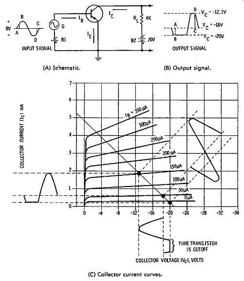
Fig. 6-1. Cutoff limiting using pnp transistor. (A) Schematic. (B) Output
signal. (C) Collector current curves.
Next, let us consider the second alternation in Fig. 6-1. The input voltage aids the forward bias produced by the base-emitter battery B1. As a result, the forward voltage is increased, thereby increasing the emitter current. Both the collector and base currents are increased by corresponding amounts. increased collector current flowing through the load resistor increases the voltage drop across the resistor. Thus, the collector voltage Ve rises (becomes less negative) to -12.1 volts. This effect is seen in the output waveform at B. As the input signal starts to decrease (CD), the output waveform begins to go more negative. During the entire negative alternation, the in put signal aids the forward bias. The output signal is positive- going, although, as shown, the entire output signal is negative due to the applied -20 volts.
The extent of cutoff limiting in the signal is determined chiefly by the forward-bias value. However, the type of transistor, as well as the input circuit resistance and input-signal amplitude are also determining factors that affect the amount of cutoff limiting. A decrease in the forward-bias voltage shifts the operating point to a lower value of quiescent base current, thereby increasing the amount of cutoff limiting. Increasing the forward bias shifts the operating point to a higher value of quiescent base current, thereby decreasing the amount of cutoff limiting. If the input signal in Fig. 6-1 should be reduced to a very small amplitude, the limiter would operate as a CE amplifier.
SATURATION LIMITING
The circuit in Fig. 6-2 uses a pnp transistor connected in a CE amplifier configuration, and biased for saturation limiting.
During the first (positive) alternation, the input signal voltage opposes the forward bias supplied by the base-emitter battery Bl. The resultant forward voltage is decreased, thereby decreasing the emitter current. Both the collector and base currents are decreased by corresponding amounts. The decreased collector current flowing through load resistor Rr. produces a smaller voltage drop across Rr., Collector voltage Ve changes from a no-signal value of -1 volt to -6 volts as shown in Fig. 6-2B. This may be determined from the characteristic curve of the limiter circuit shown in Fig. 6-2C. For the entire half-cycle that the input goes positive, the output is negative-going. No limiting action occurs over this half-cycle.
During the second alternation in Fig. 6-2, the input signal voltage aids the forward bias produced by the emitter-base battery. The resultant forward voltage is increased, thereby increasing the emitter current. Both the collector and base currents are increased by corresponding amounts. The operating point of the circuit in Fig. 6-2C has been established on the load line above the point for class-A operation. The increase in amplitude of the input signal between X and Y does not increase the collector current, which is at saturation. Increased collector current flowing through load resistor R1 increases the voltage drop across Rr. At saturation, a steady voltage of about 15.9 volts opposes the battery voltage B2.
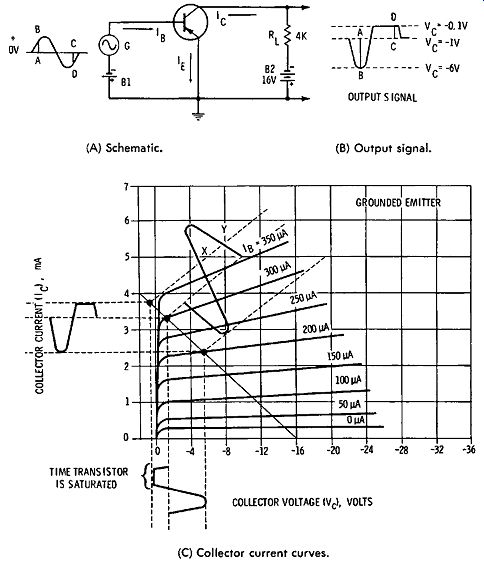
Fig. 6-2. Saturation limiting using pnp transistor. (A) Schematic. (B) Output
signal. (C) Collector current curves.
Note that the output voltage levels off at -0.1 volt in Fig. 6-2. This may be determined from the characteristic curve of the limiter circuit shown in Fig. 6-2C. Its effect, seen on the output waveform, is called saturation limiting. Increasing the for ward bias shifts the operating point to a higher value of quiescent base current, thereby increasing the amount of saturation limiting. Decreasing the forward bias shifts the operating point to a lower value of base current, thereby decreasing the amount of saturation limiting. Other factors determining the amount of saturation limiting are the type of transistor, the input circuit resistance, and the amplitude of the input signal.
Saturation limiting is employed less commonly than cutoff limiting because the transistor is operated near its maximum rated power dissipation, which complicates the design problem.

Fig. 6-3. Transistor triode limiter.
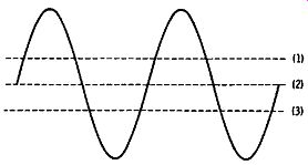
Fig. 6-4. Clipping of both positive and negative peaks.
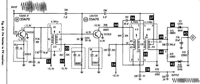
Fig. 6-5.
CUTOFF AND SATURATION LIMITING
Fig. 6-3 depicts a conventional CE amplifier circuit that can be adjusted for either cutoff or saturation limiting. When R2 is adjusted for minimum forward bias, the circuit operates as a cutoff limiter; if R2 is adjusted for maximum forward bias, the circuit operates as a saturation limiter. Again, if R2 is set to the midpoint of its range, conventional amplifier action is obtained with a small or moderate input signal amplitude. A large input signal amplitude produces both cutoff and saturation limiting, as shown in Fig. 6-4. The saturation level is indicated at (1), the quiescent level at (2), and the cutoff level at (3). Thus, a sine wave is shaped into a semi-square wave. This arrangement has the same disadvantage as noted previously for a simple saturation limiter. Therefore, it is more common practice to use a pair of cutoff limiters connected in cascade to provide both positive and negative peak limiting.
When a square wave is to be formed by limiting a sine wave, successive amplification and clipping must be utilized to obtain fast rise. Because numerous transistors and associated components are required, it is usually preferred to generate square waves directly by means of multivibrators, as explained previously. However, limiters serve a unique purpose, for example, in fm radio receivers, and in the sound sections of TV receivers. Fig. 6-5 shows a limiter arrangement for a TV receiver. This is a diode-transistor cascade limiter. Diode XS conducts on negative peaks, and thereby limits the negative excursion of the signal by short-circuiting the input circuit of the transistor. Positive peaks are applied to the base of transistor Q10, thereby providing cutoff limiting. Subsequent limiting action is provided by the ratio detector.
TRANSISTOR CLIPPER CIRCUITS

Fig. 6-6. Negative peak clipper.
We have seen that a limiter rejects the positive peak, negative peak, or both positive and negative peaks of a waveform.
On the other hand, a clipper passes either the positive peak or the negative peak, and rejects the remaining portion of the waveform. For example, Fig. 6-6 depicts a negative-peak clip per. The base-emitter junction of the transistor is normally zero-biased. However, when an input signal is applied, the base draws current on negative half-cycles. This causes the coupling capacitor to charge and produce positive signal-developed bias on the base. Therefore, the transistor is reverse biased with signal present. Between negative input-signal peaks, some of this bias leaks to ground. The amount of decay depends on the RC time constant of the base circuit.
It follows that the input signal in Fig. 6-6 will produce sufficient base conduction on each negative peak to replace the charge decay. In turn, the amount of clipped-peak waveform that appears in the collector circuit depends on the RC time constant of the base circuit. The extent of clipping also depends on the input signal level. At very small input levels, al most one-half cycle is passed into the collector circuit; however, at high signal levels, only a small portion of the peak drive waveform passes into the collector. This basic arrangement is widely used in sync-separator configurations, as shown in Fig. 6-7. Note that the negative sync tips are stripped from the video signal, amplified, and passed into the collector load.
The normal DC voltages in the absence of signal in Fig. 6-7 provide forward bias of 0.2 volt on Q13. An average video signal applies 1 volt pk-pk drive to the base of the transistor.
Signal-developed bias reverse-biases the base-emitter junction, and only the negative sync tips can drive the transistor into conduction. Because the video-signal level varies from one channel to another, it is desirable to have bias regulation to maintain the clipping point at the black level of the video signal. This is the function of diode X38. When the signal level is high, the diode conducts more, or its internal resistance decreases. In turn, the emitter bias voltage becomes less negative, and part of the signal-developed bias is effectively can celled. Thereby, the clipping point of the transistor tends to "follow" the black level in the video signal.
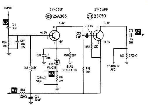
Fig. 6-7. Peak clipper used as sync separator.

Fig. 6-8. Unit step waveforms, showing formation of a pulse.
TRANSISTOR SWITCH WAVE-SHAPERS
Pulse and switching waveshapers are used in television, radar, telemetering, pulse-code, and computer equipment. In this Section, we are concerned chiefly with the basic features of transistor switch waveshapers. Pulse and switching circuits are normally characterized by large-signal, or nonlinear operation of a transistor. Circuit operation usually entails a driving pulse, which might be generated by a blocking oscillator, for example. The circuit develops a discontinuous change in voltage level or current level. That is, the input waveform (trigger pulses) produces output signals that have large and sudden changes in voltage or current. We will find that the output waveform may differ considerably from the input wave form. A switching circuit has two states: the transistor is either cut off, or it is in collector saturation.
Trigger-pulse waveforms are illustrated in Fig. 6-8. For simplicity, these are shown as ideal waveforms with zero rise and fall times. A voltage that undergoes a sudden change in amplitude from one level to another is called a unit step voltage. In pulse and switching-circuit application, when the unit step voltage is the applied signal, it is commonly of sufficient amplitude to cause the circuit to change from a conduction state to a cutoff state, or vice versa. In turn, a unit step voltage in the output section of the circuit results from the change of state.
In Fig. 6-8, a positive unit step voltage waveform is shown at A. At time t1, the voltage level is increased positively by an amplitude V. This voltage level does not necessarily have to increase from zero to its maximum value. If the initial voltage was at a negative potential, and then changed to zero, note that a positive unit step voltage would be produced. Fig. 6-8B depicts a negative unit step voltage. At time t2, the voltage level is decreased by an amplitude V. In this example, the change in level could be from a high positive potential to a lower positive potential. Fig. 6-8C depicts a square or rectangular pulse waveform. At time t1, the voltage level is increased by an amplitude V. Between t1 and t2 , a new constant voltage level is established. At time t2, the voltage level is decreased by an amplitude V. Thus, a square pulse can be described as formed by two unit step voltages, one of which is positive and the other negative.
When a transistor is operated in the switching mode by a pulse-input waveform, it may be regarded basically as an over driven amplifier, being driven alternately from cutoff into collector saturation, and vice versa. A transistor switch is analogous to a relay. Various circuit configurations have associated advantages and disadvantages. The CE output characteristics of a typical pnp transistor are shown in Fig. 6-9A. These characteristics are arranged in three regions: cutoff, active, and saturation. An arbitrarily chosen load line and the maximum permissible power dissipation curve are also shown.
We consider the cutoff and saturation regions to be the stable or quiescent regions of operation. A transistor is considered to be in the off (nonconducting) or on (conducting) state when it is operated in the cutoff or saturation regions, respectively. The third region of operation, called the active region, is the unstable (transient) region through which operation of the transistor passes while changing from the off state to the on state.
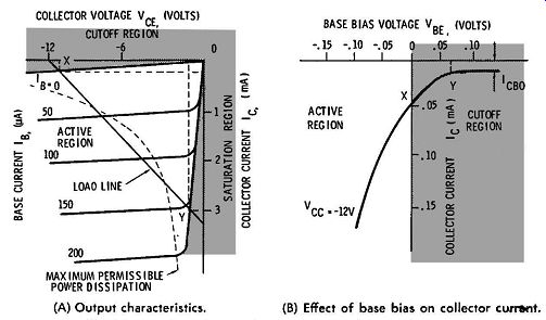
Fig. 6-9. Transistor characteristic curve switching application.
(A) Output characteristics. (B) Effect of base bias on collector current.
(A) Conventional schematic.
(B) Diode equivalent circuit.
(C) Switch equivalent of circuit.

Fig. 6-10. Transistor switching circuits.
The effect of base-bias voltage Vin: on collector current I" in the cutoff and active regions is shown in Fig. 6-9B. A typical transistor switching circuit is shown in Fig. 6-10A. Switch S1 represents a pulse waveform source, such as a blocking oscillator. It controls the polarity and amount of base current from battery V11 1 or V11~- Resistors R11 1 and R11~ are current limiting resistors. The emitter-base and collector-base diode and switch equivalent circuits representing the off and on ( dc) conditions of the transistor switching circuit are shown in Fig. 6- 10B and C. Note that although a CE configuration is depicted in Fig. 6-10, we may employ any of the three basic configurations shown in Fig. 6-11. These various circuits have advantages and disadvantages in switching applications, as explained subsequently.
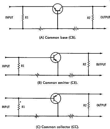
Fig. 6-11. Basic amplifier configurations. (A) Common base (CB). (B) Common emitter
(CE). (C) Common collector (CC).
The cutoff region in Fig. 6-9A includes the area above the zero base-current curve On= 0). Ideally, with no base current flow, there would be zero collector current. That is, the collector voltage would equal the battery voltage V cc in Fig. 6- 10A. However, at point X on the load line in Fig. 6-9A, a small amount of collector current flows. (See the horizontal projection to the collector-current axis.) This is more clearly indicated in Fig. 6-9B, where, at zero base-bias voltage (point X), the collector current le equals approximately 0.05 ma. This is the reverse-bias collector current for the CE configuration.
Note that the application of a small reverse base-bias voltage VnE (approximately 0.075 volt), reduces the value of reverse bias collector to the value of Icno- We recall that the significance of Icno is as shown in Fig. 6-12.

Fig. 6-12. l_cbo measurement.
Collector voltage V cE in Fig. 6-9A is indicated by the vertical projection from point Y to the collector-voltage axis. This value is equal to the difference in magnitude between the battery voltage (12 volts in this example) and the voltage drop produced by reverse-bias collector-current flow through load resistor RL in Fig. 6-l0A. Normal quiescent conditions for a transistor switch in this region require that both the emitter base junction and collector-base junction be reverse-biased.
With S1 in its off position, the emitter-base junction is biased by V112 via RB2. This is comparable to application of a positive unit-step voltage. The collector-base junction is reverse-biased by V cc via RL; the transistor is in its off state. We will find that a switching circuit is designed to produce very fast transition between its off and on states.

Fig. 6-13. Limiter and switch waveshaper circuit for horizontal-output stage.
Both limiting and switching circuits are commonly used in cascade for horizontal deflection of a picture tube. For example, Fig. 6-13 shows a limiter stage that is driven by the output from a blocking oscillator. The output waveform is limited to form a rectangular pulse. This pulse drives a power-output transistor connected in a switching arrangement. Note that the output transistor Q22 is reverse-biased; this is a signal developed bias produced by base-current flow on drive peaks that charge C33. The chief requirement is that Q22 be driven with great rapidity from its off state to its on state, and vice versa.
In the diode equivalent circuit of the transistor in Fig. 6- 10B, diodes XE and Xe represent the emitter-base and collector-base junctions, respectively. Diode X1s is reverse-biased by V1m; diode Xe is reverse-biased by Ven- Ideally, there is no current flow through RL, and V f'1s equals Vee- The circuit thus rep resents an open switch, as depicted in Fig. 6- 10C. That is, the initially applied bias causes S1 and S2 to open the output circuit. The active linear region shown in Fig. 6-9A is the only region that provides conventional amplifier action. In the linear region, the collector-base junction is reverse-biased, and the emitter-base junction is forward-biased. Transient response of the output signal is essentially determined by the transistor characteristics in this region. In a switching circuit, this is called the transition region.
Operation of S1 in Fig. 6-10A to its on position is comparable to the application of a negative unit-step voltage. Forward bias is established by Vni, via R111, and Iii and le become transitory, moving from point X in Fig. 6-9A along the load line to point Y. Here, collector current reaches saturation; the signal passes through this region rapidly. Note that load line A passes through the maximum power-dissipation curve. This is permissible because the excursion of collector current through the "forbidden region" is very rapid, so that the average power dissipation is low through the forbidden region and does not damage the transistor.
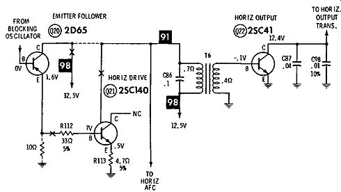
Fig. 6-14. Emitter follower used as an impedance-matching device.
Some horizontal-deflection systems include an emitter follower that serves as an impedance-matching device, as shown in Fig. 6-14. It provides improved power-transfer efficiency, although an extra transistor is required. Good efficiency is desirable to minimize battery drain. Note that in the saturation region shown in Fig. 6-9A, an increase in base current does not cause an appreciable increase in collector current le, At point Y on the load line, the transistor is in its saturation region. le, measured by the horizontal projection from Y, is at a maximum, and VcE, which is measured by vertical projection from Y, is at its minimum value. This value of collector voltage is called Vsat• Excessive or "deep" saturation is undesirable, because it tends to distort the output waveform, as explained subsequently in greater detail. The saturation region is also called the bottomed region of the transistor.
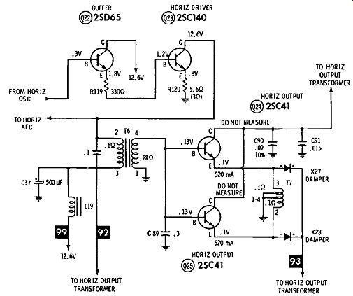
Fig. 6-15. Paralleled transistors provide double power output.

Fig. 6-16.
In Fig. 6- 10A, when le reaches its limited value, the transistor saturates and is in its on state. In the diode equivalent circuit of Fig. 6-10B, XE and Xe are forward-biased. XE is for ward-biased by V BE. The saturation voltage V cu drops to a smaller negative value than V BE; the difference of these voltages produces the forward bias V rn on Xe, That is, the equivalent switch circuit is closed. S1 and S2 close the circuit for Ve(' via Rr,. The circuit is switched from the on state to the off state in a similar manner. Small input voltage or current pulses can control large output voltage or current pulses. If greater power output is required than can be provided by a single transistor, two transistors are often paralleled, as depicted in Fig. 6-15.
Another method of obtaining greater output power is to use a silicon controlled rectifier instead of a horizontal-output transistor, as shown at X28 in Fig. 6-16. An SCR is analogous to a thyratron, as a transistor is analogous to a triode tube.
That is, an SCR can be gated into conduction, but will not thereafter cease conduction until the output voltage swings to zero. That is, the input gating pulse cannot bring the SCR out of conduction. It is often more economical to use an SCR as a gated control switch than two or more transistors connected in parallel.
We also find horizontal-output transistors connected in the CC configuration, as shown in Fig. 6-17. All three of the basic configurations shown in Fig. 6-11 may be operated in the switching mode. The CB configuration operates as a series switch. The collector output current is a large percentage of the emitter input current. For practical purposes, we may consider these two currents to be equal. The transient response of the CB arrangement is better than that of the other basic circuits. However, impedance matching may present a problem because the input resistance is low and the output resistance is high.
The CE configuration operates as a shunt switch. That is, the base input current merely controls the collector output current. Transient response is poorer than that of the CB arrangement. However, it has high power gain, and impedance matching usually imposes fewer problems. Next, the CC con figuration also operates as a shunt switch. Its voltage gain is practically unity. The CC switch is easily driven because of its high input resistance. Its low output impedance is well adapted to loads that draw heavy ac currents. A CC switch is usually driven near, but not into its saturation region because both input and output resistances change greatly in the saturation region, which causes difficulties in avoiding output waveform distortion.
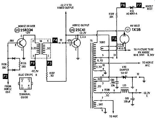
Fig. 6-17. Horizontal-output transistor connected in CC configuration.
QUIZ
1. Name the three basic types of limiters.
2. How is cutoff limiting accomplished?
3. Explain how saturation limiting is provided by a transistor.
4. Describe combination cutoff and saturation limiting action.
5. How can a semiconductor diode and a transistor provide limiting of both signal peaks?
6. Discuss the operation of a negative-peak clipper that uses signal-developed bias.
7. Distinguish between a limiter circuit and a clipper circuit.
8. Define a unit step voltage waveform.
9. What is the basic characteristic of a transistor switch waveshaper?
10. Explain the action of trigger pulses in a switching circuit.
11. Define the cutoff, active, and saturation regions of a transistor.
12. Which are the stable regions of operation?
13. Identify the unstable region of a switching transistor.
14. Describe the basic IcBo measurement.
15. Define the on and off states of a switching transistor.
16. Why is a limiter often used to drive a switching transistor?
17. What is the advantage of driving a switching transistor with an emitter follower?
18. Explain why a pair of switching transistors may be operated in parallel.
19. Describe the function of a silicon controlled rectifier.
20. What advantage does an SCR offer in a horizontal-output system?
21. Name the three basic transistor switching configurations.
22. State the chief features of a CB switching circuit.
23. What are the basic characteristics of a CC switching con figuration?
24. Compare a CE switch with a CC switch arrangement.
25. Why is a CC switch ordinarily driven short of saturation?