AMAZON multi-meters discounts AMAZON oscilloscope discounts
In the first analysis, the basic principles of scope application and waveform evaluation developed in preceding Sections apply to transistor electronic computers. However, we will find that more sophisticated concepts are involved, because computers are designed to operate at maximum practical speeds.
We are concerned with the fastest possible rise and fall times, the maximum practical repetition rates, and the minimum practical pulse widths. We work with circuits that have the greatest practical bandwidth, and semiconductor devices that have the fastest response time attainable. We are concerned with problems of deterioration in pulse waveshape, and processes for pulse regeneration. Moreover, reliability of circuit action must approach 100 percent, even if speed of operation is sacrificed. Let us consider some of the problems of pulse circuit action encountered in transistor computers.
(A) Transistor switching circuit. (B) Diode equivalent of circuit at (A). (C) Switch equivalent of circuit at (A).
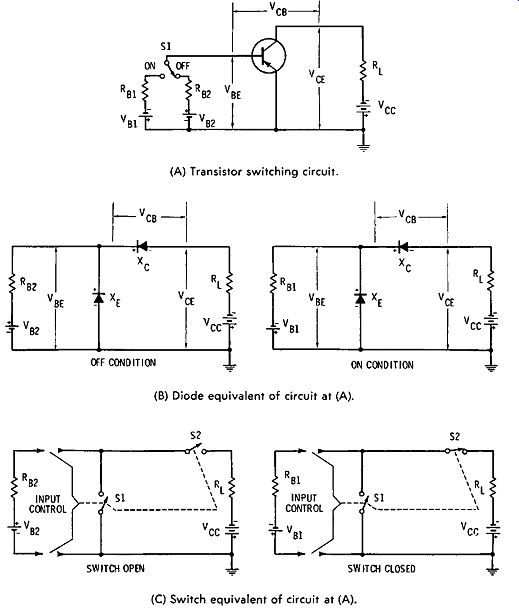
Fig. 1. Analysis of transistor switching circuit.
Fig. 1 illustrates a simple transistor switching circuit.
(A) Input current pulse.
(B) Output current pulse.

Fig. 2. Current pulse characteristics.
When S1 is thrown from off to on, and then back to off, an input current pulse waveform I_B is generated, as shown in Fig. 2A. In this large-signal operation, the input waveform In drives the transistor from cutoff to saturation, and back to cutoff. The output current pulse le in Fig. 2B is formed, differing from IH because a transistor cannot respond instantly to a change in signal level. This waveform indicates the transient response of the switching circuit. It is evident that the transient response of a transistor basically determines the maximum repetition rate (switching speed) at which the circuit may be operated. That is, the transistor is generally the bottleneck in limitations of switching speed. The output pulse characteristics are governed basically by the ac characteristics of the transistor.
RISE-TIME CONSIDERATIONS
We know that rise time is measured between the 10-percent and 90-percent points on the leading edge of a waveform. Factors affecting rise time are the nonlinear characteristics of the transistor, the energy storage in the semiconductor substance, and, in some cases, the characteristics of the external circuit.
Charge carriers (holes or electrons) moving from emitter to collector in the transistor do not have completely free flow paths. The charge carriers collide occasionally with semiconductor atoms, and become dispersed and diffused. Therefore, all charge carriers that start out do not reach the collector output terminal at exactly the same time. We will find that overdriving a transistor results in decreased rise time. Therefore, overdrive is minimized in practical switching circuits.
Rise time is denoted by t, in Fig. 2B. Following the rise interval, the pulse waveform attains a maximum value for the so-called pulse time, t1 " as depicted in Fig. 2B. The pulse time is also called the duration time of the waveform, and denotes the length of time that the pulse remains at or near its maximum value. Pulse-time duration is measured from the point on the leading edge where the pulse has attained 90 percent of its maximum value, to the point on the trailing edge at which the amplitude has fallen to 90 percent of its maximum value.
STORAGE TIME
The storage time is denoted by t. in Fig. 2B. This is also called the minority carrier storage time. When the input current I_B is cut off, the output current le does not fall to zero instantaneously, but remains at almost maximum value for a certain length of time before decaying to zero. This storage time is also referred to as saturation delay time. It results from injected minority charge carriers that are present in the base region of the transistor at the moment when the input current is cut off. We recall that electrons are minority carriers in p material, and that holes are minority carriers in n material. These charge carriers have a certain mobility, and require a certain length of time to be collected. Transistors with specialized internal construction are used to minimize switching time.
Holes have a mobility of 1700 cm/sec per volt/cm; electrons have a mobility of 3000 cm/sec per volt/cm. Therefore, it is advantageous to use npn transistors in switching applications, because electrons are then minority carriers in the base region, and electrons have a comparatively high mobility. The length of the storage time depends on the degree of saturation into which the transistor is driven, and the time that the charge carriers spend in saturation. The base-current In reversal that occurs between points X and Y in Fig. 2A at the end of the input pulse, is the result of the stored carriers contributed by the current gain of the transistor, multiplied by the initial in put current I_B.
When this current value decays to a value equal to the maximum current value at saturation, the collector-base junction becomes reverse-biased, and both Ia and Ir thereafter decay exponentially to zero. We recognize that for high-speed switching, storage time is undesirable. Minority carrier storage can be avoided by switching a transistor from its off state to a point in the active region, thereby avoiding collector saturation.
We will find that a technique called collector clamping can be used to prevent operation of a transistor in its saturation region.
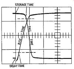
Fig. 3. Superimposed display of rise and fall times by triggered-sweep scope.
FALL TIME
In the fall time, or decay time, of a pulse we know that the amplitude decreases from 90 percent to 10 percent of its maximum value. The fall time of a pulse is determined by essentially the same factors that determine its rise time. We will find that fall time can be reduced slightly by application of a re verse current at the end of the input pulse. Fig. 3 shows a superimposed display of rise and fall times by a triggered sweep scope. The turnoff time of a switching transistor is the sum of its storage time and fall time. Decreased turnoff time results from decreasing either the storage time or the fall time.
If the turnoff time is decreased, the maximum permissible switch rate (repetition rate) is thereby increased.
In transistor switching applications, the output current should be zero when the transistor is cut off. However, zero output current cannot be realized in practice. In the CB con figuration of Fig. 4A, with the emitter current equal to zero (IE = 0), a small reverse-bias collector current flows. This current is produced by minority carriers in the collector and base regions. Reverse-bias collector current le-no results from thermal generation of electron-hole pairs, and this current increases with temperature. In the CB configuration, the value of le-Bo, also called leakage current, is normally quite small and is measured in microamperes. Consequently, it can be tolerated in most applications.
(A) lcac,. (B) lcEo

Fig. 4. leakage current.
In the CE configuration of Fig. 4B, leakage current I«'Eo from emitter to collector is much larger than in the CB configuration. ICEo is measured from collector to emitter with the base terminal open (h = 0). Note that Ic-EO stems from Ic-no That is, reverse-bias minority carriers ( electrons, solid-line arrow) in the collector region enter the base region and combine with holes ( dashed-line arrow) from the emitter region.
Before combining, however, the electrons cause a heavy hole current to flow from emitter to collector. In other words, the electrons from the collector region act as a base-bias current to cause an amplified collector-current flow. The magnitude of this current is approximately the product of beta and Ic1m Since beta ranges from 25 to 50 for typical switching transistors, leakage current is of major concern.
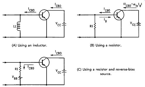
Fig. 5. Circuits for reduction of leakage current lc1m, (A) Using an inductor.
(B) Using a resistor.
R1 (C) Using a resistor and reverse-bias source.
REDUCTION OF l_ceo
The value of Icim can be reduced by means of several circuit arrangements. However, we cannot reduce Inm below the value of Il'no, As shown in Fig. 5A, an inductor, L1, may be used instead of a base-return resistor. In turn, there is negligible DC voltage drop between base and emitter, and when In= 0, In,o = lc,110. It is not always possible to use an inductor in a switching circuit; accordingly, a low-valued resistor, R1, may be used instead, as depicted in Fig. 5B. Flow of I_CBO through R1 produces a small forward bias, resulting in a small flow of base-emitter current In. In turn, Ic,m is approximately equal to beta times In. To minimize In, the value of R1 is made as small as is practical. When a high base-input resistance is required, IcEo can be minimized by means of a reverse-bias source V_BB, as shown in Fig. 5C. This reduces I_B to zero, so that only the leakage current I_cbo flows.
In a properly designed switching circuit, and with a transistor in normal operating condition, the rise and fall times are comparatively rapid. A collector load resistance of 500 ohms is typical (not shown in Fig. 5). The drive waveform may have an amplitude of 0.5 volt pk-pk, with a source resistance of 50 ohms in a typical switching circuit. A collector supply voltage of 3.5 volts may be utilized. The output pulse waveform will have a typical amplitude of 7 mA pk-pk and a peak-to-peak voltage of 3.5 volts. This drive condition switches the transistor from cutoff to collector saturation. Corresponding rise and fall times are illustrated in Fig. 6; the time base of the scope is set for 0.5µs per horizontal division.
(A) Rise time. (B) Fall time.

Fig. 6. Rise time and fall time in switching transistor.
CUTOFF AND SATURATION CLAMPING
When a transistor is driven to saturation and cutoff, the output waveform may be distorted. Variations in collector potential occur when either the temperature-dependent cutoff current drifts, or the load impedance varies. The resulting change in collector potential can cause unreliable operation of following stages. We know that when a transistor is driven into saturation, minority-carrier storage delay occurs. This widens the pulse waveform and reduces the permissible repetition rate of the switching circuit. Junction diodes are commonly employed to avoid transistor operation in saturation, or at cutoff.
Other methods are also used to avoid objectionable saturation.
In Fig. 7, a pnp transistor is used in the CE configuration for a simple switching circuit. Drive current In is sufficiently great to drive the transistor from cutoff to saturation without the clamping diodes X1 and X2, and bias batteries V,,., and Yes- Fig. 7B shows the transistor output characteristics with load line R1,. V,-c is 12 volts in this example. X1 and bias battery Vco are used for cutoff clamping. X2 and Yes are used for saturation clamping. Clamping of the upper and lower levels in the output waveform facilitates substitution of one transistor for another. Since operation with clamping diodes usually provides operation over the linear portion of the output characteristics, low cutoff current and low saturation voltage are eliminated. The average power dissipation is increased, and the load line must be selected so that transistor operation falls within the permissible power-dissipation region, under the maximum power-dissipation curve noted previously.
(A) Schematic. (B) Characteristic curves.
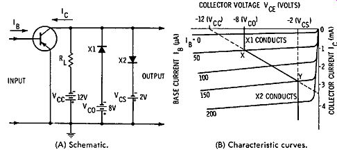
Fig. 7. Cutoff and saturation clamping.
Let us consider cutoff clamping action. In Fig. 7B, we may assume that Itt has started to fall from 150µA at point Y. The collector voltage increases negatively from 2 volts at this point.
Battery V co applies 8 volts to XL As the collector potential increases from 2 volts toward 8 volts, X1 remains reverse biased and nonconducting. When the collector potential reaches point X ( Ill= 50µA) on the load line (8 volts), X1 becomes forward-biased and starts to conduct. Fig. 8 depicts ideal and approximate practical clamp characteristics. Further decrease in In toward zero has no effect on the collector potential, which remains fixed at 8 volts, even though le decreases (Vco holds V cE at 8 volts).
(A) Ideal characteristic. (B) Approximate practical characteristic.
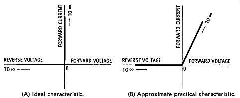
Fig. 8. Clamp characteristics.
Current flow through RL in Fig. 7 is maintained at X (about 1 mA); it consists of Ir and the current through for ward-biased XI and V rn, The voltage drop across RL is equal to the difference (approximately 4 volts) between Vee and V co- Any change in Ic that does not cause it to exceed the value at point X is compensated by current from Vee- Thus, equilibrium is established and the output potential is fixed at 8 volts.
Note that X2 is reverse-biased and is effectively an open circuit in the foregoing clamping process. In high-speed switching circuits, the transient response of diodes becomes a matter for consideration.
(A) Single diode. (B) Double diode.

Fig. 9. Collector-to-base saturation clamping.
Next, let us follow the circuit action in saturation clamping.
Disregarding X1 and Vco in Fig. 7, we may assume that In is increased to 150 µ A at point Y. The collector voltage, indicated by the vertical projection to the collector-voltage axis, falls to 2 volts. The voltage drop, produced by increasing le through RL, causes the collector voltage to fall. Bias voltage from V cs is 2 volts. A slight further increase in Ic, due to increase in h, further decreases the negative potential on the collector, and forward-biases X2, which starts to conduct.
When X2 conducts, its resistance is very small, and V.,s is effectively applied between collector and ground. This voltage can not change and since it is in parallel with Ve., and R1,, the voltage across this branch cannot change. Current through R1, is fixed to provide the necessary voltage drop so that the collector-to-ground potential is equal to Yes- In this example, the load current is approximately 3 mA. Although the collector current may increase further, because of an increase in base current, the collector potential remains fixed at 2 volts. Additional collector current is drawn from V<•s through X2. The vertical extension of the load line from Y rep-resents the zero-resistance load line for forward-biased X2.
The normal load line, on the other hand, extending from Y to the collector-current axis (dashed line) would enter the saturation region, which falls beyond the knee of the curve of 111 = 200µA. The collector-base diode would be forward-biased in this region. When the drive current is reduced to zero, I<' falls rapidly from its maximum value to point Y, and then follows the normal load line toward point X. However, any minority carrier storage introduced by the clamping diode (Fig. 7)
would affect the width of the output pulse. To the left of point Y on the load line, the collector potential is more negative than 2 volts. Diode X2 is reverse-biased, and is therefore in a non conducting state.

Fig. 10. Deteriorated pulse-drive waveform.
Thus, the foregoing switch circuit provides combination clamping. The effect of cutoff and saturation clamping is to keep the collector potential in the range of -2 to -8 volts, thereby preventing waveform distortion due to cutoff and saturation conditions in the transistor. More efficient switching action can be obtained by means of collector-base saturation clamping with a single diode or a duo-diode. Single-diode clamping is depicted in Fig. 9A. In the cutoff condition of the transistor, X1 and the emitter-base junction are reverse-biased by R1, R2, and R_B in series with V_cc· and V_BB When V_cc and V_BB are equal, R1 + R2 is made slightly greater than RB. This provides the required initial reverse bias for the emitter-base junction. R1 is much larger than R2, the ratio being determined by the desired clamping voltage when the transistor is conducting.
It is assumed that the drive pulse to the switching circuit has a more nearly ideal waveshape than can be reproduced in the collector circuit. Pulses become progressively deteriorated, as shown in Fig. 10. Therefore, computer systems employ waveform regenerators when necessary, to reconstitute approximately ideal drive waveforms. Details of pulse regeneration are explained subsequently. Let us assume that l 1 x in Fig. 11A forward-biases the emitter-base junction, and drives the transistor into saturation. The potential at the junction of R1 and R2 is negative, and is effectively fixed near the very low saturation voltage of the transistor. The collector voltage falls from V_cc·to this fixed potential. X1 is nonconducting and I_B = I_N = I_C, and is the amplified drive potential I_IN. When the collector potential falls just below the fixed potential, X1 conducts.
As X1 conducts and I1 x increases further, Ill remains essentially constant, and the excess current is shunted through R2 and X1. I(' increases by the small value of excess current input, rather than by the amplifier input current prior to clamping action. Since relatively small currents are passed through X1, the minority-carrier storage delay contributed by the clamping diode is smaller than that contributed by the clamping diode in Fig. 7. Battery power dissipated in R1 and R2 is avoided by using double-diode clamping, as shown in Fig. 9B. X1 functions as a clamping diode, in the same manner as previously explained, while X2 substitutes for R2 in Fig. 9A. The emitter-base junction is reverse-biased by V_BB in Fig. 9B through R_B. Collector reverse bias is provided by V_cc through L. X2 remains forward-biased throughout the circuit action. A germanium diode is generally used for X1 because it has a low forward-voltage drop. A silicon diode, with a slightly higher forward-voltage drop, is used for X2. (See Fig. 11). In a typical application, X1 in Fig. 9B provides a forward voltage drop of 1 volt, and X2 provides a forward-voltage drop of 1.2 volts. This essentially maintains a reverse bias of 0.2 volt between collector and base after clamping action ensues.
Circuit action in the duo diode arrangement is similar to that of the single-diode clamping circuit. All of the input current I1x is applied to the base, while X1 remains reverse-biased.
This condition continues until Ir. drops the collector potential just below the potential at the junction of diodes X1 and X2.
The base potential is more positive than the potential at this point by the value of voltage drop across X2. X1 becomes for ward-biased and shunts excessive input current of the collector. The smaller drop across X1 maintains the reverse collector-base bias at the difference between the drops across X1 and X2. During the clamped condition, I_L is equal approximately to beta times I_B and I_C is equal to the sum of I_L and the shunted portion of I_IN. The latter is small and contributes little to output pulse widening. Therefore, the repetition rate of the switching circuit is increased.

Fig. 11. Static characteristics of solid-state diodes. (A) Germanium diode
static characteristics. (B) Comparative diode static characteristics.
PULSE REGENERATION
A basic pulse-regenerator circuit is shown in Fig. 12. This is a one-shot multivibrator configuration; the output pulse shape is independent of the input pulse shape. Also, the width of the output pulse is independent of the width of the input pulse. Therefore, if a deteriorated pulse waveform is used to trigger the pulse regenerator, a standard pulse is obtained at the output. The common-emitter resistor contributes to fast rise and fall of the output waveform. The diode is called a steering diode, and is a one-way device that permits only a negative going leading edge to trigger the circuit. By choosing a suitable time constant, the output pulse can be made to have as narrow a width as desired, consistent with the transient response of the transistor.
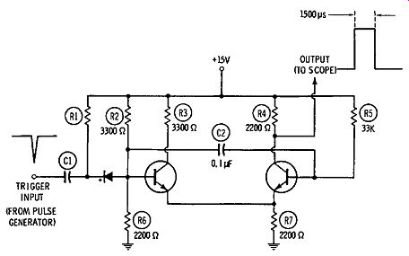
Fig. 12. Basic pulse-regenerator circuit.
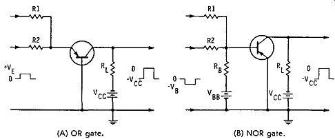
Fig. 13. Single transistor OR gates with multiple inputs. (A) OR gate. (B)
NOR gate.
MACHINE-LOGIC CIRCUITS
Machine logic is an extensive topic, and can only be briefly discussed here. Logic circuits are used in combination with counter circuits to perform operations in arithmetic. Basic transistor OR circuits are depicted in Fig. 13. An OR gate provides an output when a positive pulse is applied at either of the input resistors. That is, an output pulse is obtained by applying an input to R1 or to R2. Pulses can be applied to both resist-0rs, and an output pulse is again obtained, although the increased input current tends to produce a wider output pulse due to storage effects.
The configuration in Fig. 13B is similar to that in A, except that it is driven by a negative input pulse, and is called a NOR gate. Note that positive input pulses produce no output.
No output is obtained, whether a positive pulse is applied to R1, R2, or to both R1 and R2. However, an output pulse is obtained if a negative pulse is applied to either R1, R2, or to both R1 and R2. Fig. 14 depicts AND gates. The AND gate is similar to the OR gate, but the transistor is biased to collector saturation. An input pulse at R1 is insufficient to bring the transistor out of saturation. However, if an input pulse is also applied to R2, the sum of input 1 and input 2 then drives the transistor from saturation and into cutoff. Thus, inputs 1 and 2 together produce an output pulse. The NOT AND gate provides a negative output pulse when positive pulses are applied simultaneously to the inputs. However, no output is obtained with negative applied pulses.
(A) AND gate. (B) NOT AND gate.
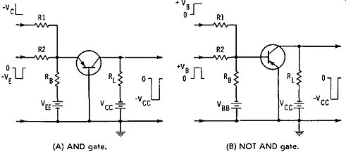
Fig. 14. Single transistor AND gates with multiple inputs.
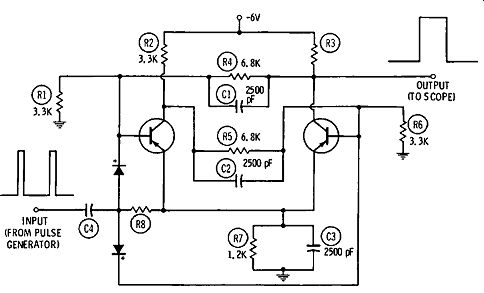
Fig 15. Flip-flop configuration with trigger circuit.
A flip-flop circuit is shown in Fig. 15. This is the basic element in a counter section, and is used for information storage in electronic computers. It is basically a bistable multivibrator, and requires two input trigger pulses in succession to produce an output pulse. Therefore, the repetition rate of the output pulse is one-half the repetition rate of the input pulses.
It is evident that if we connect two flip-flops in series, one output pulse will be obtained for four input pulses. Three flip-flops connected in series provide one output pulse for six input pulses, and so on. If neon bulbs are connected in the collector circuits of a flip-flop chain, we obtain readout of stored binary numbers. Interested readers may refer to computer arithmetic books for discussion of binary numbers and their relation to ordinary decimal numbers.
The diodes in Fig. 15 are steering diodes that direct input pulses automatically to the transistor that should be triggered for proper flip-flop action. The transistors conduct alternately from one input pulse to the next, and the diodes are alternately reverse-biased by the circuit voltages, so that each pulse flows into the correct transistor. C1 and C2 are speedup capacitors, used to obtain maximum speed of response. They overcome the integrating effects of R4 and R5. C3 is a conventional emitter bypass capacitor. R7 serves as a temperature-stabilizing resistor. Direct coupling is used in computer flip-flops to minimize the number of components that are required.
QUIZ
1. Explain the distinction between a switching circuit and an amplifier circuit.
2. What is the cause of input pulse distortion in a switching circuit?
3. What are the causes of output pulse distortion in a switching circuit?
4. Why is overdrive minimized in pulse switching circuits?
5. Discuss the meaning of storage time in a switching transistor.
6. Do electrons or holes have greater mobility?
7. How is leakage current IcEo minimized in a switching circuit?
8. State typical voltage and current amplitudes in a switching circuit.
9. What rise and fall times might we find in a switching circuit?
10. Define cutoff and saturation clamping.
11. Discuss the effect of storage time in a clamping diode.
12. Why are two diodes often used in a saturation clamping circuit?
13. Describe deterioration of a pulse waveform in a computer system.
14. Briefly explain the differences in forward characteristics of semiconductor diodes.
15. How is a one-shot multivibrator used as a pulse regenerator?
16. Explain the configuration of an OR gate.
17. How is a NOR gate distinguished from an OR gate?
18. Describe the configuration of an AND gate.
19. How does a NOT AND gate differ from an AND gate?
20. What is the function of machine logic?
21. Discuss the operation of a flip-flop counter section.
22. Why are flip-flops connected in cascade?
23. How is information stored in a counter chain?
24. Explain how readout can be obtained from a counter chain.
25. Is readout obtained in the binary system or in the decimal system?