
Fig. 3-1. Coaxial cable prevents pickup of stray fields.
A scope has appreciable input capacitance, which is about 20 or 30 pF at the vertical-input terminal. Test leads or a coaxial cable must be connected to the input terminal for actual test work (Fig. 3-1). Unshielded test leads may not be suitable for testing in tv signal circuits, such as the grid of a video amplifier or sync separator. The unshielded leads often pick up excessive hum voltage and flyback pulse interference. It is standard practice, therefore, to make all scope tests with a coaxial input cable to the vertical-amplifier terminals.
When a coaxial input cable is used, the total input capacitance to the scope becomes about 100 pF. This capacitance does not cause objectionable circuit loading when testing across a cathode resistor, for example, but it will disturb many video and sync circuits seriously.
Fig. 3-2 shows how a sync pulse can be distorted objectionably by shunting excessive capacitance across the circuit under test. The total input capacitance to the scope is imposed when a direct probe (straight-through connection) is used.

Fig. 3-2. Typical result of circuit loading. (A) Display of a normal (B) Signal
distorted by video signal. integration.
LOW-CAPACITANCE PROBE
It is standard practice to use a low-capacitance probe instead of a direct probe, in order to avoid waveform distortion caused by circuit loading. The most common type of low-capacitance probe is a compensated attenuating device. This type of probe reduces the signal voltage and, in turn, the input capacitance to the scope. Most probes are adjusted to attenuate the signal voltage to 0.1 of its source value, and to reduce the scope input capacitance to 0.1 of the value imposed by a direct probe. The input impedance to the scope is thus effectively increased ten times.
Configuration
A typical configuration for a low-capacitance probe is shown in Fig. 3-3. The values of R1 and R2 depend on the scope's input resistance, typically 1 megohm. The probe does not stand alone in actual operation, for R2 is shunted by the scope's input resistance. Thus, if R2 has a value of 1 megohm, its effective resistance value will become 0.5 megohm when it is connected to the input cable of the scope.
In order to get a 10-to- 1 attenuation, R1 is made nine times the effective value of R2. R 1 is therefore 4.5 megohms for the example cited. The total input resistance to the probe (when connected to the cable) is 5 megohms. The voltage drop across R2 equals 0.5/5, or 0.1 of the input voltage to R1. Thus, a 10-to- 1 attenuation occurs. This attenuation is observed only at low frequencies, such as 60 Hz, because the input capacitances of the cable and scope have a greater by-passing effect on higher frequencies.
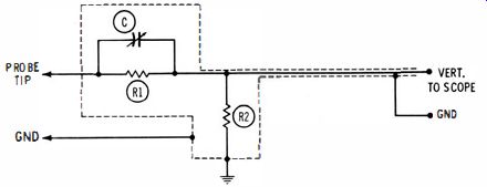
Fig. 3-3. Low-capacitance probe.
The probe must be compensated in order to obtain proper attenuation and distortionless signal passage. This is the function of trimmer capacitor C. The probe will have a 10-to- 1 attenuation at high frequencies when C is adjusted correctly. The time constant of C and R1 must be equal to the time constant of the effective input resistance and capacitance to the scope. As a practical example, assume that the input capacitance at the cable is 100 pF. The time constant to the scope is then 0.5 X 10^6 multiplied by 100 X 10^-12, or 50 X 10^-6 second. Thus the time constant is 50 microseconds. Hence, the time constant of R1 and C must also be adjusted to 50 microseconds.
Inasmuch as R1 has a resistance of 4.5 megohms, C must have a value of about 11 pF. A trimmer capacitor is used so that an exact adjustment can be made.
Adjustment
There are two principal methods of adjusting a low-capacitance probe. The first makes use of square waves. If a 15-kHz square wave is fed from a square-wave generator to the low-C probe, the reproduced square wave will change shape on the scope screen as C is adjusted. When the capacitance is too high, the square wave appears differentiated. When it is too low, the square wave appears integrated.
Correct adjustment of C provides distortionless reproduction of the square wave.
Not all square-wave generators provide a perfect output. It is advisable first to check the generator waveform by connecting the direct probe of the scope to the generator output terminals. Observe the waveform and then duplicate this waveform with the low-C probe connected to the scope input cable. The probe can be adjusted properly regardless of generator distortion. It is necessary only to reproduce the same waveform applied by the generator.
The second method of probe adjustment is a two-frequency test.
For example, a 60-Hz sine-wave voltage is applied to the probe, and the resulting vertical deflection noted. Next, a 15-kHz sine-wave voltage is applied to the probe from an audio oscillator. The audio oscillator is set for the same output voltage as in the 60-Hz test. Also, capacitor C is adjusted to give the same vertical deflection on the scope screen as before. Output voltages at 60 Hz and at 15 kHz can be checked with the scope, using a direct probe.
Most service scopes are suitable for operation with low-C probes, but there are a few exceptions. A scope must have a step attenuator which provides a fixed value of input resistance and capacitance on each step in order to operate properly with a low-C probe. However, a low-C probe cannot be matched to a scope which has merely a potentiometer for the vertical-gain control. While the probe can be adjusted for proper response at one gain setting, another gain setting may not match the probe and therefore distortion results.
Low-capacitance probes are useful over the frequency response range of the scope. If the scope has a flat response from 20 Hz to 2 MHz with a direct probe, it will have the same frequency response when a low-C probe is used. The probe does not change the existing frequency response of a scope, but merely steps up the input impedance. For these reasons, a low-C probe is used to test sync, video amplifier, horizontal-oscillator and afc, and sweep circuits. The frequencies in these circuits range from 60 Hz to 15 kHz, plus harmonic frequencies up to 1 or 2 MHz.
The permissible voltage which may be applied to a low-C probe is the same as for a direct probe. Because conventional scopes have blocking capacitors rated at 600 volts, this is the maximum input voltage permissible with a direct probe. Similarly, the components used in commercial low-C probes are not rated for more than about 600 volts. When higher peak-to-peak voltages are to be tested, another type of probe should be used to avoid possible damage to both scope and probe. High-voltage probes are explained later in this SECTION.
Why are low-C probes generally designed with a 10-to- 1 attenuation factor? This factor ties in with the decade step attenuators on modern scopes. Recall that once a scope has been calibrated with a known peak-to-peak voltage, recalibration is not required when the step attenuator is turned to another position; the decimal point in the calibration factor is merely shifted to the left or right, as the case may be. If the scope is calibrated using a direct probe, it is likewise not necessary to recalibrate if a 10-to-1 low-C probe is to be utilized next.
The decimal point in .the calibration factor is shifted one place to the right.
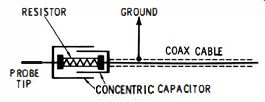
Fig. 3-4. Lab-type low-capacitance probe.
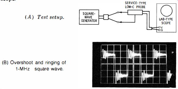
Fig. 3-5. Square-wave test showing the effect of using a service-type low
capacitance probe with a lab-type scope. (A) Test setup. (B) Overshoot and
ringing of 1·MHz square wave.
Use a Lab-Type Probe With a Lab-Type Scope
Lab-type low-capacitance probes utilize concentric construction, as shown in Fig. 3-4. In other words, the probe construction follows the basic plan of a coaxial cable. This construction permits display of fast -rise waveforms with very little distortion. For example, a square wave or pulse with a rise time of 0.02 microsecond passes through a lab-type probe with practically no overshoot or ringing.
On the other hand, a service-type low-capacitance probe is constructed with ordinary components and has no coaxial configuration.
In turn, fast-rise waveforms are distorted by the residual inductance of the components and connecting wires. When a typical service-type low-C probe is used with a lab-type scope, a 1-MHz square wave with a rise time of 0.02 microsecond is displayed. The result is a large amount of overshoot and ringing, as illustrated in Fig. 3-5. Therefore, good practice requires that a lab-type probe be used with a lab-type scope.

Fig. 3-6. Reading peak-to-peak voltage from vertical-gain setting.

Fig. 3-7. Read the instantaneous voltage at a point along the waveform.
Note that the vertical attenuators in lab-type scopes are calibrated in peak-to-peak volts. Since the vertical amplifier is very stable, reliance can be placed on the indicated calibration values over long periods of time. A low-C probe, when used with the scope, customarily reduces the input voltage to the vertical amplifier by a factor of 10. Fig. 3-6 depicts calculation of the peak-to-peak voltage; we note the peak-to-peak voltage reading of the vertical attenuator, multiply it by the number of centimeters of vertical deflection, and finally multiply this value by the attenuation factor of the probe (usually 0.1). Sometimes the instantaneous voltage of a waveform is of interest.
In other words, we wish to measure the peak-to-peak voltage at a particular point along a waveform. Fig. 3-7 shows an example of a staircase waveform in which we wish to measure the peak-to-peak voltage of the fourth step. We proceed to note the peak-to-peak voltage reading of the vertical attenuator, and multiply this reading by the number of centimeters from the base line of the waveform to the fourth step. Finally, we multiply this value by the attenuation factor of the probe (usually 0.1). Demodulator Probes
Technicians commonly make tests in circuits operating at 20 MHz, 40 MHz, or even higher frequencies even though service scopes have a top frequency limit of I or 2 MHz, or occasionally 4 or 5 MHz.
In order to display waveforms in high-frequency circuits, a demodulator probe is used (Fig. 3-8). It is a special form of detector probe that operates on the same principle as a detector in a tv receiver. The rectifier and its associated circuitry recover the modulation envelope from the high-frequency carrier. This envelope contains video frequencies to which a scope can respond. The response of an ordinary demodulator probe is not as good as that of a video detector in a tv receiver. The reason is that a probe must have a fairly high input impedance to avoid undue circuit loading. A demodulator-probe circuit, therefore, is like that in Fig. 3-8, instead of like a video-detector circuit. If a demodulator probe were constructed with the circuit principles of a video detector, it would have very good frequency response. However, the input impedance would be very low, and most i-f circuits would be "killed" when the probe is applied to the circuit.

Fig. 3·8. Typical demodulator probe.
A visualization of demodulator-probe action is shown in Fig. 3-9.
This is an idealized presentation. In practice, the corners of the output waveform are rounded, and the rise and fall intervals of the waveform are slowed down. Thus, after a horizontal sync-pulse signal passes through a conventional demodulator probe, it become" substantially distorted, or "feathered."
MODULATED IF SIGNAL

Fig. 3-9. Visualization of demodulator-probe action.
While it is possible to devise wideband demodulator probes that do not distort horizontal sync pulses, these probes require a cathode follower tube as an electronic impedance transformer. This makes a wideband probe somewhat complicated and expensive. Therefore such probes are usually not used outside of laboratories. In service work, the probes are simple and comparatively inexpensive. These provide usable information even though video signals are substantially distorted.
A compromise between circuit loading and waveform distortion is sometimes made by the use of a demodulator probe such as the one shown in Fig. 3-10. This configuration imposes somewhat greater circuit loading than the probe in Fig. 3-8, but does not distort the horizontal sync pulses so much. The technician must not expect, however, to obtain perfect reproduction of video signals with a simple demodulator probe.

Fig. 3-10. A compromise type of demodulator probe.
A demodulator probe is sometimes called a traveling detector, because it can be used to trace a signal stage by stage through an i-f -amplifier section. The probe is essentially an indicating rather than a measuring device. It would be an error to attempt to measure i-f stage gain with a demodulator probe. Circuit loading and detuning often change the stage response greatly, so that amplitude comparisons can be very misleading.
The maximum input voltage which can be applied to a demodulator probe is limited chiefly by the rating of the crystal diode. As a rule, no more than 50 volts peak to peak should be applied. This is not a severe limitation because demodulator probes are used customarily in low-level circuit testing, in which the signal voltage is seldom greater than 5 volts. However, should an i-f stage break into oscillation, it is possible for the oscillating voltage to exceed the probe rating and damage the crystal diode in the probe. Caution is therefore advisable.
Again do not make the mistake of using a demodulator probe when a low-C probe should be used. Fig. 3-11A shows a normal waveform in a video amplifier obtained with a low-C probe. Shown in Fig. 3-11 B is the seriously distorted waveform displayed when by mistake a demodulator probe is used instead. Here are the rules:
1. When the signal frequency falls within the response range of the scope, always use a low-C probe.
2. When the signal frequency is higher than the response range, always use a demodulator probe.

Fig. 3-11. Do NOT use a demodulator probe in video-amplifier circuits. (A)
Normal waveform, using low-C (B) Distorted waveform, using probe. demodulator
probe.
Do not be confused by the observation that a distorted waveform can sometimes be seen when a low-C probe is applied at an i-f amplifier grid or plate. In theory as applied here, nothing should be seen because the i-f frequency is much higher than the response range of the scope. What actually happens is that the i-f amplifier is being overdriven by the i-f signal. As a result, the tube is driven into grid current. The amplifier tube operates as a partial detector under this abnormal condition of operation.
RESISTIVE ISOLATING PROBE
A resistive isolating probe is a simple device consisting of a resistor connected in series with the coaxial cable to the scope (Fig_ 3- 12). This probe is used only in sweep-alignment procedures. It is basically a low-pass filter consisting of a series resistance feeding into a shunt capacitance (cable capacitance). The probe is a simple integrating circuit.

Fig. 3-12. A resistive isolating probe.
This probe sharpens the marker indications on a response curve, and helps to remove noise interference when making low-level sweep tests. The probe must have a suitable time constant for satisfactory operation. When the time constant is too long, the response curve is distorted and the marker position (if the marker is on the steep side of a curve) is displaced. On the other extreme, broad markers result when the time constant is too short. In general, a 50K resistor with a conventional coaxial cable gives a good response in sweep-alignment work.
It is sometimes thought that a resistive isolating probe could be used in place of a low-capacitance probe in testing sync circuits, video-amplifier circuits, etc. However, this is a misconception. The low-pass filter action of the resistive isolating probe weakens or wipes out the high frequencies in such waveforms, imposes phase shifts, and greatly distorts the sync or video waveforms. This probe is also unsuitable for i-f amplifier tests. If applied to i-f circuits, nothing is displayed on the scope screen, because the i-f signal is "killed" by the probe before it gets to the scope.
HIGH-VOLTAGE CAPACITANCE
DIVIDER PROBE High peak-to-peak voltages occur in the horizontal -sweep section of a tv receiver. These voltages will arc through a low-C probe, damaging both probe and scope. A special probe therefore is required to test these high ac voltages. A typical circuit is shown in Fig. 3- 13.
This is a capacitance-divider arrangement. When two capacitors are connected in series, an applied ac voltage drops across the capacitors in inverse proportion to their capacitance values. Thus, if one capacitor has 99 times the capacitance of the other, 0.0 1 of the applied voltage is dropped across the larger capacitor. In turn, the smaller capacitor requires a high voltage rating.

Fig. 3-13. Typical high-voltage capacitor-divider probe.
The attenuation factor of the probe is 100-to-1, and is set by a trimmer capacitor. This is a maintenance adjustment. A 100-to- 1 factor is used to tie the probe attenuation in with the decade step attenuator of the scope. The probe attenuates horizontal sweep-circuit signals to 0.01 of their source value, thus protecting the scope against damage. If the scope has been calibrated with a direct probe, it is not necessary to recalibrate when a high-voltage probe is to be used. The decimal point in the calibration factor is shifted two places to the right.
The high-voltage probe is useful in any horizontal-frequency circuit test. However, it attenuates the usual sync-circuit and horizontal oscillator voltages too much for convenient observation. Its use is therefore generally restricted to the horizontal-sweep circuit. Beginners sometimes erroneously use a high-voltage capacitance-divider probe in 60-Hz circuits, such as the vertical-sweep circuit. Vertical frequency waveforms are distorted by the probe, as shown in Fig. 3-14.
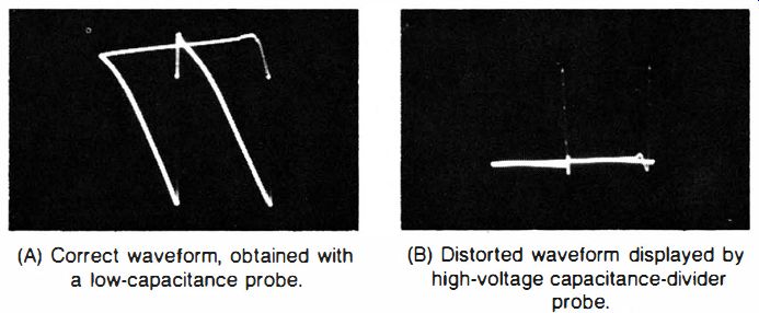
Fig. 3-14. Distortion of 60-Hz waveform by high-voltage capacitance-divider probe.
(A) Correct waveform, obtained with a low-capacitance probe. (B) Distorted
waveform displayed by high-voltage capacitance-divider probe.
The reason for this distortion is seen from Fig. 3-15. The probe does not stand alone, but works into the vertical-input impedance (Rin and Cn) of the scope. The shunt resistance can be neglected at horizontal frequencies, because it is very high compared with the low reactance of the input capacitance. But, at vertical frequencies, the shunt resistance has a value on the same order as the reactance of the input capacitance. The probe thus acts as a differentiator at vertical frequencies, and vertical-frequency waveforms are badly distorted.
When a low-C probe or a high-voltage capacitance-divider probe is used, the waveform aspect is the same as with a direct probe. In most scopes, the beam is deflected when a positive voltage is applied to the vertical-input terminal, and vice versa. When a demodulator probe is used, the waveform aspect is determined by the polarity of the crystal diode in the probe. If the diode is reversed, a positive-going sync display will be changed to a negative-going display, as shown in Fig. 3-16.
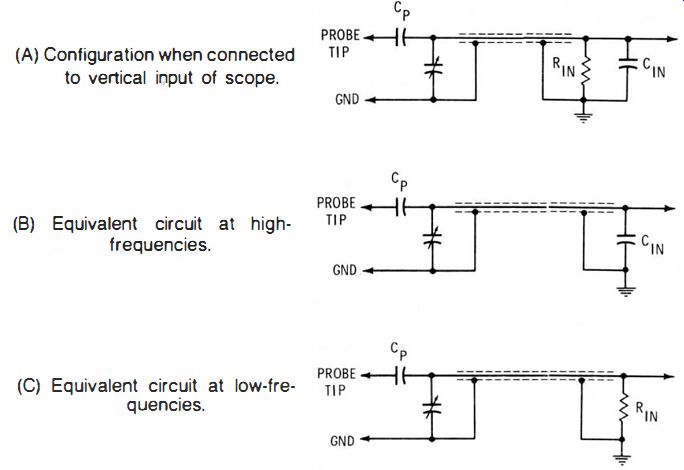
Fig. 3-15. High-voltage capacitance-divider probe and its load circuit. (A) Configuration
when connected to vertical input of scope. (B) Equivalent circuit at high frequencies.
(C) Equivalent circuit at low-frequencies.
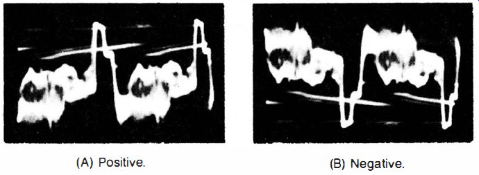
Fig. 3-16. Positive- and negative-going video signals. (A) Positive. (B)
Negative.
A few scopes have a polarity-reversing switch, making it possible for the user to invert the pattern. If a negative-going pulse is displayed when a demodulator probe is used and the operator prefers to invert the display, it is then necessary only to turn the polarity-reversing switch. Its chief use is in sweep-alignment displays (Fig. 3-17). Some technicians prefer to work with positive-going curves, and a polarity reversing switch makes the curve aspect independent of detector polarity.

Fig. 3-17. Sweep-alignment curves. (A) Positive-going curve. (B) Negative-going
curve.
STRAY FIELDS
Exposed binding-post connections, even though a shielded input cable is used to the scope, can be a source of hum or horizontal-pulse pickup when a low-capacitance or demodulator probe is used. The reason for this is that the vertical-input terminal becomes a high
impedance point regardless of the circuit impedance under test. Coaxial connectors therefore are preferred to binding posts. A coax connector provides a completely shielded connection which is immune to stray fields.
Do not be confused by the stray-field pattern which appears when a direct or low-capacitance probe (or unshielded test leads) are left unconnected on the bench (Fig. 3- 1 8). The stray-field pattern disappears if the probe or leads are connected across a resistor, capacitor, or inductor. Appearance of the stray-field pattern on open circuit is due to the high input impedance and high sensitivity of the scope.
Stray fields are a source of very high impedance voltages. When the input impedance to the scope is reduced by connecting the input leads or probe across a component, stray fields induce a negligible voltage into the leads.
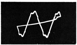
Fig. 3-18. Stray-field pattern, displayed when test leads of scope are left
open.
If a low-C probe is connected to a very high impedance circuit, however, and stray fields are fairly strong, the probe tip will sometimes pick up enough stray-field interference to be troublesome. This situation is infrequent, but when it does occur, the stray-field interference can be minimized by removing the alligator clip from the end of the probe, so that a minimum pick-up surface is exposed. A clip can be used without difficulty in most tests. This is convenient because the probe does not have to be held in contact with the circuit point under test.
Most stray-field problems are external to the scope itself, but sometimes distortion of waveforms results from internal difficulties. An example is false deflection of the base line at the left-hand end when the scope is operated at high gain. This results from cross talk between the blanking and the vertical step-attenuator circuits in most cases.
Scopes susceptible to this type of distortion sometimes operate normally when the blanking function is not used. The difficulty can be corrected by enclosing the vertical step attenuator in a grounded shield can.
Base-line distortion may be observed even when the blanking function is not used. This results from cross talk between the horizontal deflection and vertical step-attenuator circuits. The only remedy is to enclose the step-attenuator components in a shield box, as mentioned.
Sometimes an unstable vertical amplifier in a scope will simulate stray-field interference. For example, if the scope does not have input cathode followers, parasitic oscillation may occur in the pattern when testing across a coil with the scope operating at high gain. Most service scopes have input cathode followers. Those service scopes without cathode followers may need to be operated with caution when testing resonant circuits which can form a tuned-plate tuned-grid oscillator in combination with the peaking coils in the first vertical amplifier stage. This applies principally in signal-tracing sound i-f circuits, which resonate at 4.5 MHz.
INCONSISTENT LOW-C PROBE RESPONSE
Sometimes when a low-C probe is adjusted for proper response on one setting of the step attenuator, its response is poor on another setting. This generally results from improper adjustment of the compensating trimmers in the step attenuator. (Refer to Fig. 2-15.) In case C2 or C3, or both, are misadjusted, probe response will be inconsistent on different attenuator steps. Both incorrect attenuation factor and waveform distortion can result.
To check the adjustments of the compensating trimmers in a step attenuator, it is most convenient to use a square-wave signal with an approximate IS-kHz repetition rate. The trimmers are set so that good square-wave reproduction is obtained on each step.
Basis of Bandwidth Requirement
Audio amplifiers step up voice and musical frequencies. The range of these frequencies can be simply demonstrated by connecting a speaker to the vertical-input terminals of a scope. The waveform of any sound entering the speaker will be seen on the scope screen. If the speaker output transformer is used, connect the primary terminals to the scope input terminals. Much weaker sounds are then reproduced. Analysis of various speech and musical tones will show that a top frequency of about 10 kHz and a lower limit of about 20 Hz is necessary for full reproduction of sound. This is the bandwidth requirement of an audio amplifier.
Video i-f amplifiers step up modulated i-f signals. The basis of the bandwidth requirement is illustrated in Fig. 3-19. A modulated sine wave has sideband frequencies. They can be separated individually from the modulated wave by narrow bandpass filters, such as those in amateur radio gear. The "spread" of the sideband frequencies determines the bandwidth requirement of an i-f amplifier. For example, consider a 40-MHz carrier wave modulated by a 4-MHz video signal. The modulated wave consists of the 40-MHz carrier, a 44 MHz sideband, and a 36-MHz sideband. A form of single-sideband transmission and reception is used in tv transmission, so that the i-f amplifier need have a bandwidth of only 4 MHz, instead of 8 MHz.
For the example cited, the i-f amplifier would pass the 40-MHz carrier and the 44-MHz sideband.

Fig. 3-19. Build-up of a modulated sine wave.
GROUND LEAD OF SCOPE PROBE
Do not overlook the necessity for a suitable ground return when making oscilloscope tests. Consider the simplest situation (Fig. 3-20) in which an unshielded test lead is connected from the vertical-input terminal of the scope to the circuit under test. Excessive hum voltage appears in the pattern, as shown, because no ground lead is connected between the scope case and the chassis of the receiver under test. The hum voltage appears because the ground-return path is forced to route itself through the power supplies of the receiver and scope via the 117 -volt line. The hum interference disappears when a ground lead is connected from the scope case to the receiver chassis.
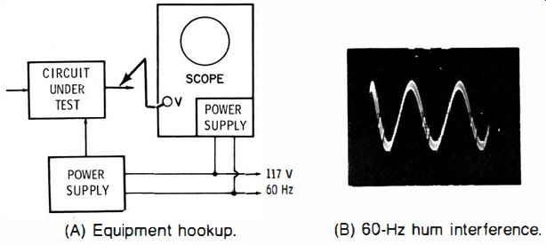
Fig. 3-20. Effect of omitting ground-return lead. (A) Equipment hookup. (B)
60-Hz hum interference.
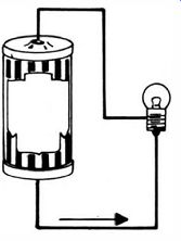
Fig. 3-21. If one of the leads is omitted, the lamp does not light.
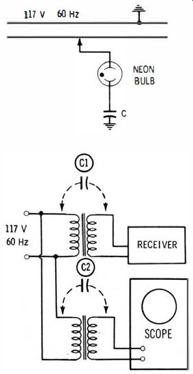
Fig. 3-22. Capacitor provides return path.
Fig. 3-23. Stray capacitances C1 and C2 form a high-Impedance "connection" between the receiver chassis and scope case.
The need for a complete circuit is plainly evident in the case of direct current, as in Fig. 3-21. If one of the leads is omitted, the lamp does not light. However, capacitance can complete a ground-return circuit in an ac configuration (Fig. 3-22). The reactance of capacitor Cat 60 Hz permits alternating current to flow through the neon bulb.
The bulb glows, although there is not a complete metallic path around the circuit. (Note that one side of the power line is always grounded, as a protection against lightning.) The higher the capacitance of C, the brighter the lamp glows.
Both the receiver and the scope shown in Fig. 3-23 have power-supply transformers. There is stray capacitance between the primary and secondary of each transformer. Although there is no ground lead connecting the receiver chassis and the scope case, a high-impedance "connection" nevertheless exists between them, because of stray capacitances C1 and C2. There is a small capacitive transfer of 60-Hz current from primary to secondary via C1 and C2. It is so small that it is generally regarded as being of no importance. Nevertheless, if a ground-return lead from the scope to the receiver chassis is mistakenly omitted, forcing a ground-return path through C1 and C2, the small 60-Hz voltage drop across each of stray capacitances C1 and C2 will appear in the pattern.
In the case of a demodulator probe, it is essential to use the short ground lead which is connected to the probe housing. Technicians sometimes suppose that if an open ground lead is run from the scope to the receiver chassis, there is no need to bother with the short high-frequency ground lead of the probe. This is a serious error for the following reason. Unless· the high-frequency ground lead is kept quite short, its series inductance and stray capacitance will act as a filter and seriously disturb the high-frequency signal. At 40 MHz, for example, the signal may be killed completely. If a long ground lead permits some i-f signal to pass, the waveform is likely to be highly distorted.
The need for using the short ground lead provided with a low capacitance probe is less important. But, when testing video wave- forms (which have frequency components up to 4 MHz), waveform distortion can occur unless a reasonably short ground-return lead to the probe is used.
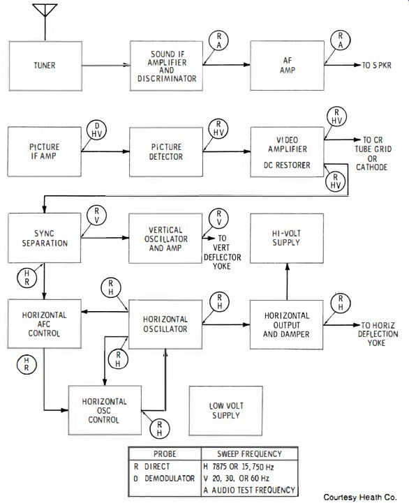
Fig. 3-24 Simplified block diagram for a tv receiver, showing test points.
Fig. 3-24 is a simplified block diagram of a typical black-and-white tv receiver. It shows the various stages and test points for application of the scope probe. The letters at each test point indicate the correct type of probe to use, and also indicate the approximate setting of the scope sweep frequency. For clarity, all amplifier stages are included within one block in the diagram of Fig. 3-24. However, tests may be made at input terminals or output terminals of individual amplifier stages, by using the indicated probe and sweep-frequency setting.
Note that at any point up to the video detector, the signal voltages will be quite small and considerable vertical gain will be required. On the other hand, within the sync and deflection circuits, signal voltages are comparatively high and much less vertical gain is required. Of course, under trouble conditions, the normal signal amplitude may be greatly weakened, or no signal voltage may be found at the test point.
When making tv receiver tests, remember that two basic frequencies are involved in the video signal. The vertical or field frequency is 60 Hz. In turn, any test of circuit action (except that within the horizontal oscillator and its differentiator network, or in the horizontal-amplifier stages) can generally be made with a sweep frequency of 20 or 30 Hz, thus displaying two or three complete fields of the signal. To test horizontal pulse shapes or horizontal -deflection circuit action, the sweep frequency should be set at 15,750 or 7875 Hz. This sweep rate will display one or two complete cycles of the waveform.
As a general preliminary test, the point-to-point method of signal checking is most helpful because receiver malfunction is often caused by loss of all or a significant portion of the picture information and pulses at some stage along the signal channel.