Surprisingly Low-Cost Lab Supply
The µA723, as first introduced by Fairchild, is one of the oldest and most accepted regulator ICs in the industry. The µA723 is second-sourced by almost every linear IC house in the U.S. and still enjoys enormous usage.
Thus, this IC has become about as inexpensive as a linear IC can be. The µA723 equivalent circuit is shown in Fig. 13-1.
Because \ref (the internal reference voltage) is about 7 volts, the µA723 is usually configured in one of two basic circuits-one for output voltages below 7 volts and the other for output voltages above 7 volts.
These basic circuits are shown in Fig. 13-2. The usual external current increasing transistors are not shown here, in order to keep the circuits simple.
One of the linear IC houses which makes the equivalent of the µA723, Teledyne, has published an application note in which is shown a novel circuit that allows output voltages above and below 7 volts. That basic circuit is shown in Fig. 13-3. This circuit has in it a correction that was made from the original (which would have prevented the current limit from functioning). A complete lab-regulated supply providing 2 to 20 volts DC with current limiting at 300 mA is shown in Fig. 13-4, with an NPN power transistor to increase current capability. The IC pin connections in Fig. 13-4 are for the dual inline package version of the µA 723 only; the "TO-5 can" packaged 723 would work as well, but pin numbers would have to be changed. The rectifier-filter section utilizes a Triad F91X transformer and a full-wave rectifier with capacitor input. The rectifier diodes are Motorola HEP R0051s, but almost any two 1 amp silicon rectifier diodes ( 1N4002s, for instance) could also be used. Q1 is a Motorola HEP S5000, but it has several equivalents-RCA SK3041, Sylvania ECG152 or 2N5191.
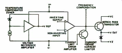
Fig. 13-1. Equivalent circuit.
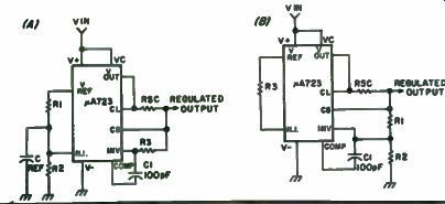
Fig. 13-2. Basic low-voltage regulator (Vout = 2 to 7 volts). Basic high-voltage
regulator (Vout = 7 to 37 volts).
All the parts are board mounted, with the exception of the transformer, filter capacitor and 25k voltage-control pot. In off-board mounting of the 25k pot (say on the front panel of one's own power supply cabinet), the lead lengths of the wires to the pot should be minimized.
It is intended that the AC switch, fuse holder, meters (if used) and binding posts also be mounted on the cabinet housing the circuit board. LMB and Bud each have a line of small box cabinets that would be suitable for making a finished bench supply using this circuit. The choice of which particular cabinet will usually be dictated by the meters one has on hand, because the circuit board is only 2" x 2 1/2 ". An LMB W1N box cabinet ( 10" x 4" x 3 1/2 ") was used for the metering circuit shown in Fig. 13-5. Only meters that were on hand were used.
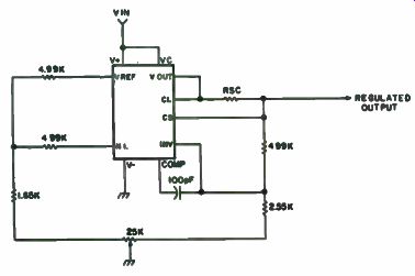
Fig. 13-3. Basic wide output voltage regulator circuit with 723.
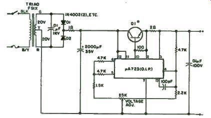
Fig. 13-4. Regulated lab supply. D1, D2 = Motorola HEP R0051; Q1 = Motorola
HEP S5000. Heat sink with washer and silicone grease.
For all its use of inexpensive or available parts, this regulated supply has more than proven itself on the bench. The 2-volt lower limit allows even RTL and low-voltage CMOS logic to be operated from the supply, and the 20-volt maximum output voltage allows for most other logic and linear IC circuits.
Adjustable Bench Supply
How about constructing an adjustable voltage power supply that can have up to 1.5 amperes output with good load voltage regulation and full overload protection at minimal cost? Admittedly, a $5 estimate depends a lot on what parts are available from one's junk box, but for just a few dollars spent on a new IC, one can have the "heart" of a very versatile power supply.
The new IC is the LM317 by National Semiconductor. This IC promises to be as famous as the LM309, which is universally used in power supplies for digital circuitry.
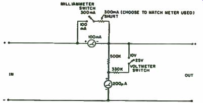
Fig. 13-5. Metering section.
The new LM317 is an adjustable, three-terminal positive voltage regulator. Its simple external connections rather belie the complexity and performance features of the unit. As shown in Fig. 13-6, it has only simple in/out connections and a minimum of three simple external components are required. The output voltage is set by the ratio of two resistors, R1 and R2.
By making R2 variable, one can adjust the output voltage to be any value from a few volts less than the DC input voltage to the regulator down to a minimum of about 1.2 volts output. Thus, if the input DC voltage were 40 volts, the output voltage can be continuously varied from about 37 volts down to 1.2 volts.
Although the output voltage is determined only by a resistor setting, the output voltage is regulated at any given setting. The regulation will be about 0.1 percent going from no load to full load (1.5 amperes, assuming the transformer/rectifier used for the DC input voltage handles this current). The LM317 is also overload and thermally protected. If the current limit is exceeded, such as by short circuit, the LM317 will simply "shut down." If the regulator gets too hot, either because of excessive load current and/or inadequate heat dissipation, it will also protect itself. Although one can destroy the LM317 like any other IC, it is pretty hard to do with any sort of reasonable care.
The manufacturer suggests two additional capacitors (C2 and C3) be used, which may prove useful in some applications. C2 is used to bypass the adjustment terminal to ground to improve ripple rejection. This bypass prevents ripple from being amplified as the output voltage is increased.
About 60 dB ripple rejection is achieved without this capacitor, but it can be improved to about 80 dB by adding it. A 10 mF or greater unit can be used, but values over 10 mF do not offer any significant advantage in further ripple improvement. The manufacturer particularly recommends the use of a solid tantalum capacitor type since they have low impedance even at high frequencies. An alternative is the use of the more readily available and inexpensive aluminum electrolytic, but it takes about 25 mF of the latter type to equal 1 mF of the tantalum type for good high frequency bypassing. C3 is added to prevent instability when the output load presents a load capacitance of between 500 and 5000 pF. By using a 1 mF bypass at the output (solid tantalum again or aluminum electrolytic equivalent), any load capacitance in the 500 to 5000 pF range is swamped and stability is ensured. Both the C2 and C3 will not be required for many applications where the LM317 is being used with a specific load circuit. But is the LM317 is used as the heart of a general purpose bench type power supply, they should be included.
Figure 13-7 shows a PC board layout and component placement diag ram. This layout has been suggested by the manufacturer, but there is no need to follow it exactly as long as all of the external components are grouped around the regulator with solid short leads. The diagram show the LM317 in a TO-220 plastic case which is designated the LM317T. Most amateurs will probably prefer to buy the LM317 in the familiar TO-3 metal case and, in this case, it is the LM317K. But, when using the unit, note an important difference as compared to the old LM309K. The case on the ...
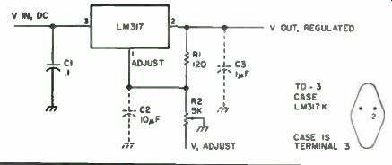
Fig. 13-6. Basic adjustable voltage regulator circuit using an LM317. Normally
only three external components are needed, but C2 and C3 may be useful in certain
situations as explained in the text.
... LM309K was ground so one could simply bolt the thing down on a chassis for heat sinking. The case on the LM317K is the output terminal, so it must be properly insulated from a chassis.
Various power supply ideas and considerations can suggest themselves for the LM317. For instance, R2, instead of being a variable resistor, can be replaced by switchable fixed resistors to obtain some of the commonly used supply voltages such as 6, 9, 12, 15 volts, etc. This idea, plus a continuously variable output voltage position, is featured in the practical realization of a power supply using the LM317 as shown in Fig. 13-8. This supply will deliver fixed output voltages of 6, 9, 12 and 15 volts (depending upon how the trim potentiometers are set), plus a continuously variable output of 1.2 Fig. 13-7. This is a PC board layout for the regulator suggested by the manufac turer. R2 is shown as a multi-tom pot for ease of adjustment. The figure also shows the pin connections for an LM317 if it is obtained in the TO-220 plastic case.
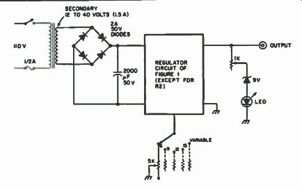
Fig. 13-8. A complete power supply using the LM317. The switch simply selects
different 5k Ohm pots which are set for 6, 9, 12, 15, and a variable voltage
output.
The latter 5k pot is front panel mounted. The function of the LED is described in the text to about 24 volts. All outputs can deliver at least 1.5 amperes with the components specified. The supply is simple to build in any size metal enclosure suitable for the components used. The only precautions to ob serve are to firmly heat sink the LM317 to one side of the metal enclosure and to keep the 0.1 mF capacitor going from pin 3 to ground, the 10 mF capacitor going from pin 1 to ground and the 120 ohm resistor going between pins 2 and 1, all connected directly at the LM317 terminals. The other components may be mounted wherever it is convenient to do so. The zener diode/resistor/LED combination at the output of the supply serves as a crude but useful voltage output indicator without having to build a regulator voltmeter in the supply. The LED just starts to glow when the output voltage is about 9-10 volts (depending on the tolerances of the components used). The 1k resistor is adjusted so the LED just glows fully when the maximum output voltage is reached. So by using the fixed output voltage positions (which are adjusted using a good VOM) and watching the LED, one can obtain a fairly good estimate of what the variable output voltage is set for.
Fig. 13-9. Schematic.
Easy, Quick and Inexpensive Variable DC Supply
It is extremely handy to have a source of variable DC energy in the workshop. The usefulness of this device encompasses many areas. For instance, many of today's projects are built around semiconductors which require various DC voltages. Much of the military surplus available requires either 12v DC or 24v DC sources. You may not want your final conversion to operate on this source, but it can be very helpful to see if the equipment will function on its original source voltage before converting it. Those people active as mobilers certainly could use a husky supply to test that new mobile rig. Obviously, anything that is battery operated could be run, tested or repaired with the help of this electronic wonder. It might even help you start your car some cold winter morning.
This is simply a variable autotransformer feeding a husky 30v trans former into a bridge rectifier (Fig. 13-9). The filter is a large capacitor. It would be nice to have a 30 A choke, but this filter has been satisfactory for all of these uses.
Well, now that these two major facts have been established, let's build it.
You may skip this part if you have a transformer or are going to purchase one. The transformer for this unit was a modified TV transformer.
It was the heaviest one in the junk box.
First remove the outer shell and the laminations. It may be necessary to use a little force to accomplish this. Never hit the laminations directly with a hammer. Use a mallet or a block of wood with your hammer. Take care to preserve the leads from the windings.
Next, remove the secondary windings. Generally they are the outer windings. When you remove the 6.3v filament winding, count the number of turns. It probably will consist of approximately 12 turns. Usually this type of transformer has a two turns per volt ratio. Retain this information for rewinding the secondary.
Finally, rewind the secondary. Use number 12 copper wire with a thick thermoplastic insulation, or any enamel or formvar insulated wire. As you are winding the secondary, check to be sure that the laminations will fit. You should be able to get about 60 turns on the secondary-hence 30 volts.
Using wire with thinner insulation, you can probably get several more turns.
The diodes were surplus units which were mounted on homemade heat sinks. The heat sinks were made from Vki" thick aluminum scrap. About 12 square inches were used for each diode. The heat sinks were mounted on 1 inch ceramic pillars above the chassis to promote convection. Several holes were drilled in the chassis below the heat sinks. There was a bottom plate attached and two small 24v DC surplus blowers were mounted on the back of the chassis. The output of the power supply was used to power the blowers.
Even at five volts input, the blowers would move some air. The blowers aren't necessary until the supply is run at high current output over a five to 10 minute period of time.
The toggle switch, S2, which removes the variac from the transformer and places the line voltage there instead, is used when there is a load which will greatly surpass the rating of the variac.
This unit can be used for everything from repairing transistors radios to operating dynamotor powered mobile equipment of the 12v, 30a variety.
Super Low Voltage Power Supply
You'll love this project if you have had many disasters while experimenting with unfamiliar ICs and untested circuit designs. These disasters can happen when the meter probe slips or sometimes because of the incorrect design of the circuit. In nearly all cases, however, things burn out because of excessive current drawn for too long a time. The remedy is a power supply that abruptly removes the voltage from the circuit once a preset current is exceeded. This project will be superior to the usual type of current limiting in which the power supply delivers a constant current to the load and less voltage once the current limit is reached. The objection to the latter is that the user may not be aware that the current limit has been reached and that the voltage is no longer regulated, especially if it happens for only a very brief interval. A circuit may not operate correctly with the unregulated voltage during this interval and the user would be hard pressed to discover the reason for the malfunction.
Basic Layout. Three power supplies are constructed as shown in Fig. 13-10. The first is a dual tracking supply with variable output voltage 0 to ±20 volts and current to 100 mA on each output (200 mA total current capacity). Also available is a + 12, - 6 volt option. Current sensing is done in both the positive and negative legs, and when the current exceeds a preset level, a signal is developed to shut down the output from the voltage regulator. This signal latches so that ouptut voltage can only be restored by pressing a reset switch.
The second supply has variable output from 2.6 to 25 volts and current to 1 ampere. Up to 34 volts is available at reduced current. This supply also has adjustable current sensing and, like the first supply, the output voltage shuts down when the current exceeds a preset level. Voltage is restored by pressing the reset switch.
The third supply provides a fixed 5 volt output at currents to 1 ampere for operating TTL circuits. This supply has output voltage sensing and will shut down if the voltage moves outside a preset range from 4.75 to 5.25 volts.
The first supply provides the power for the sensing circuits used in all three supplies. Also, if any one supply shuts down, the other two will shut down also.
All three supplies use voltage regulators that are short circuitproof, an added safety bonus in the event that the current sensing circuits are manually disabled or in the event of the failure of some component in the current sensing networks.
Current Sensing. The current sensing network in Fig. 13-11 operates as follows: Assume that initially no current is drawn from the supply. With
R2 set to 500 ohm, R2 + R3 = 21k and R4 + R5 = 21k.
With the wiper of R4 set closest to R3, the voltage at pin 11 of voltage comparator IC1A will be 14 volts, exactly half the voltage across C1. Assuming for the moment that no current flows in RI, the voltage across R6 and R7 will be 28 volts and the voltage at pin 10 of IC1A will be 14 volts also. When current is drawn from the positive leg of the supply, a voltage drop develops across R1 and the voltage at pin 10 of IC1A drops below 14 volts. This drives pin 13 of IC1A positive and the resulting current in R21 charges C3. QI fires, sending a pulse through C4 to SCR1. SCR1 turns on, operating relay K 1 and forcing Q2 to switch on. Q2 shorts out R27, thus reducing the output of IC3 to nearly zero volts. K1 interrupts the current to IC6 in Fig. 13-12. Q1 also sends a pulse to C14. This pulse, turns on SCR2, forcing Q4 to switch on.
This action reduces the output of IC5 to zero volts.
When the load is removed from the output of IC3, the power can be restored by opening S2A and S2B (normally closed switches). By moving the wiper of R4 closer to R5, the voltage at pin 11 of IC IA is lowered. It then requires a greater voltage drop across R1 (more current in the load at output of IC3) to lower the voltage at pin 10 of IC IA so that pin 13 will go positive.
Thus the setting of the wiper of R4 determines what current will drive pin 13 of IC1A high.
An identical network consisting of R8 to R14 and IC2 senses the current in the negative leg of the supply. The output of IC2 switches between 0 volts and - 26 volts approximately. Since IC1B will not operate normally with any input below - 0.3 volts, the voltage from pin 6 of IC2 is ...
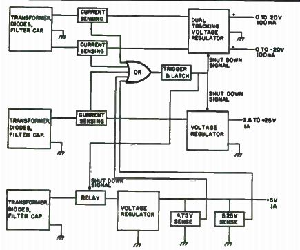
Fig. 13-10. Basic layout.
... divided down by R15 and R17 so that the voltage across R17 switches between 0 volts and - 0.25 volts. R16 and R18 form another voltage divider which provides - 0.15 volts to pin 8 of IC1B. Thus IC1B switches like IC1A in response to an overcurrent in R14. D5 and D6 form an OR gate, hence isolating the outputs of IC1A and IC1B from one another.
In Fig. 13-12, current sensing is done in the same manner as described for the positive leg of Fig. 13-11. Since the maximum current for this supply is 10 times greater than for the first supply, resistance values have been adjusted accordingly. D9 forms another part of the OR gate that feeds R21.
Voltage Sensing. For the 5 volt supply in Fig. 13-13, it is more desirable to have output sensing than current sensing. This is because there are wide variations in the current demanded by TTL circuits when they are switching from state to state. The current limit point would always have to be set rather high, and consequently only gross overcurrents could be sensed. On the other hand, a circuit that senses when the voltage falls below 4.75 volts, the lower operating limit for 7400 series TTL, is quite useful.
Suppose, for example, that you are operating near the 1 ampere limit of IC6; a brief current pulse could exceed this limit and the internal circuit of IC6 would then allow the output voltage to drop. Without voltage sensing this could easily go unnoticed and your circuit would malfunction.
In Fig. 13-13, D14 provides a reference voltage. R41 acts as a voltage divider and is set to 5.25 volts. R42 is another voltage divider and is set to 4.75 volts. IC1C and IC1D compare the output of IC6 to these voltages and, if the output moves outside the window from 4.75 to 5.25 volts, pin 1 or pin 2 will go high. This signal goes to R21 of Fig. 13-11 and eventually shuts down all the supplies.
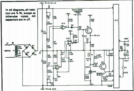
Fig. 13-11. Dual tracking regulated supply.
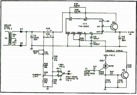
Fig. 13-12 Variable voltage power supply.
Response Time. R21 and C3 determine the response time to the circuit.
With R21= 3k and C3 = 1 uF, the circuit responds to an overcurrent, overvoltage or undervoltage that lasts 3 milliseconds or more. K1 adds an additional 7.5 ms to the time required for the 5 volt supply to shut down. By reducing C3 to 0.1 uF, response time can be made as low as 0.3 ms. R21 can be increased to as much as 10 megohms if desired to lengthen the response time, but should not be reduced below 3k.
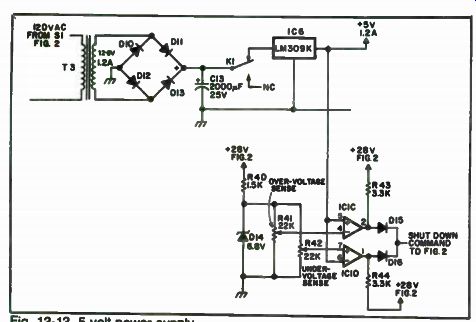
Fig. 13-13. 5 volt power supply.
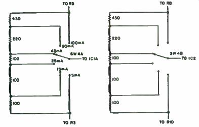
Fig. 13-14. Switch selected resistors replace R4 and R9.
The Voltage Regulators. The 419TK regulator is readily available. It is internally current limited at about 350 mA when the positive output is shorted to ground. It also has internal thermal limiting that will reduce the output when it gets too hot. A small heat sink is required when the operating current is 100 mA in each leg of the output. In Fig. 13-11, S3 is normally open. When S3 is closed, R27 can be adjusted to give + 12, - 6 volts output for the operation of certain types of voltage comparators.
The 309K also has current limiting and thermal limiting. It will provide a little over 1 ampere when mounted on a heat sink with the circuit shown.
The TVR2000 has been available from Poly Paks for a number of years and is quite inexpensive. In Fig. 13-12, a foldback current limiting option is not used. Instead, simple short circuit sensing is used. R37 and R38 set the short circuit current to a value of about 1.2 amperes. The relationship here is Rsc 1 out --- 0.1 volt, where R37 and R38 in parallel make up R.c. R39 sets the output voltage. Q3 acts as a current booster and is mounted on a heat sink.
C10 stabilizes the current limiting circuitry and C11 stabilizes the regulator section of IC5. Different values from those shown may be required to drive high capacitance loads.
Selecting Resistors. Resistors of 1 percent tolerance are best for R1, R3, R5 to R8, R10 and R12 to R14. This will make the final adjustments simpler and will keep tracking errors in R4 and R9 to a minimum. In Fig. 13-12, 5 percent resistors will suffice for R32, R34, R35 and R36, providing you choose them such that R32 R34 and R36 Regarding the tracking of R4 and R9 -since they form a tandem control, it is important that they both exhibit approximately the same resistance between their wipers and their ends for all rotations of the shaft.
Failure to do so will mean that the positive will trip at different currents. If you want very good tracking, replace both R4 and R9 with a series of 5 percent resistors and use a two pole rotary switch to select the current limit you want as shown in Fig. 13-14.
Construction. All three supplies were constructed on a single 4" x 5" printed circuit board as shown in Figs. 13-15 and 13-16. IC3 does not plug directly into the board. The holes in the board have been spaced out to assure clean etching. Solder a short wire to the outside of each pin of IC3.
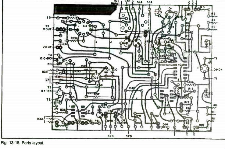
Fig. 13-15
Insert the wires into the PC board and solder. A piece of aluminum was bolted to IC3 as a heat sink. There are so many connections to the PC board from the external switches, controls, transformers, etc., that it was not possible to arrange for an edge connector on a board of this size. Instead there are about 35 wires soldered at various points around the edge of the board and all are routed to one end of the board can be hinged outward from the chassis if parts on it need to be replaced in the future.
All components fit nicely on a chassis 10" x 6" x 2".
Final Adjustments. Switch S2 to reset. Leave S3 open. This disables the shutdown mechanism. Connect a high impedance voltmeter between pin 7 of IC1D and ground. Adjust R42 for a reading of 4.75 volts. Connect the voltmeter between pin 4 of IC1C and ground. Adjust R41 for a reading of 5.25 volts.
Set the wiper of R33 to the end closest to R32. Connect a voltmeter between pin 6 of IC4 and ground. Adjust R31 so that the reading just goes to zero.
If you are using a dual potentiometer for R4 and R9, proceed as follows: Set the wiper of R4 to the end closest to R3; the wiper of R9 should then be at the end closest to R10. Connect a voltmeter between pin 13 of IC1A and ground. Adjust R2 until the reading just drops to zero. If you run out of adjustment with R2, interchange R6 and R7 and try again.
Connect the voltmeter between pin 14 of IC1B and ground. Adjust R11 until the reading just drops to zero.
If you elect to use the switched resistors in Fig. 13-13 proceed as follows: Set the switch in Fig. 13-13 to the 5 mA position. Connect a load between the positive and negative output terminals of the supply and adjust the output voltage so that the load draws 5 mA. With a voltmeter from pin 13 of IC1A to ground, adjust R2 until the voltage just drops to zero. If you run out of adjustment with R2, interchange R6 and R7 and try again. Connect the voltmeter between pin 14 of IC1B and ground. Adjust R11 until the reading just drops to zero.
Precision + 10.000v DC Voltage Reference Standard
This is a simple, easy to build DC voltage reference standard whose temperature coefficient (tempco) can be tailored to the hobbyist's individual requirements. It can be used by itself or as an individual circuit element.
Design Considerations. The circuit described uses an operational amplifier in a non-inverting circuit utilizing a single positive supply (Fig. 13-17). The output of the reference standard supplies the zener reference diode current, providing a stable supply voltage for the zener and de coupling from the positive supply voltage. The positive supply voltage should be regulated by either a three-terminal regulator or zener diode and should be from ±15 to ±18 volts.
Temperature stability is expressed in percent/°C or ppm (parts per million)/°C. (. 0001 percent/°C is equivalent to 1 ppm/°C.) A 1 ppm/°C ...
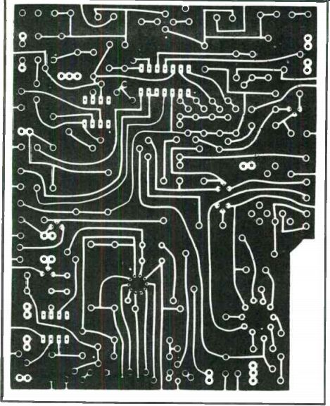
Fig. 13-16. PC board.
... change referred to an output of 10.000 volts is 10 uV/C. Both terms, percent/°C and ppm/C, will be referred to in this project.
The zener reference diode, CR1, should not be confused with the more common zener regulator diode. The zener reference diode is intended for use in applications where it is important to maintain stable DC voltages under severe combinations of temperature, shock and vibration. The temperature stability of the zener reference diode is due in part to the combination use of reverse-biased and forward-biased silicon p-n junctions, taking advantage of their opposing tempco characteristics. Application notes and design data sheets are available from the larger suppliers of zener reference diodes (e.g. Motorola, Dickson, Centrolab) and are invaluable as reference material.
The 1N821 through 1N829 family of zener reference diodes is used for CR1. The diodes in this family exhibit tempcos from 0. 01 percent/ C (1N821) to 0.0005 percent/°C ( 1N829) at a nominal zener current of 7.5 mA. The nominal zener voltage is 6.2v ±5 percent. R1, which sets the nominal zener current (7.5 mA in this case), should be a 100 ppm/°C metal film resistor. Other families of zener reference diodes can be used, such as the 1N4565 through 1N4584, with a corresponding change in nominal voltage and current.
As a general rule, the gain resistors used in the reference standard should have tempcos similar to the zener reference diode selected. For example, if the 1N821 is selected, gain resistors R2 and R3 should have tempcos of 0.01 percent/°C ( 100 ppm/°C). The overall tempco of the reference zener CR1, gain resistors R2 and R3 and to some extent, the zener current resistor R1 (providing it has a 100 ppm/°C tempco) and Al.
The gain required of the circuit is dependent upon the zener voltage.
The nominal voltage of the 1N821 is 6.2 V, necessitating a gain of 1.613 for an output of + 10.000 volts. The total resistance of R2 and R3 should be 5k to 10k, limiting the current through the gain resistors to from 1 mA to 2 mA. If R1 is a 100 ppm/°C as suggested, here is an easy way to estimate the overall tempco of the completed reference standard:
• Write down the tempcos of CR1, R2 and R3 in ppm/°C
• Square each one that you have written down
• Add the squares of R2 and R3 together, dividing the answer by seven
• Add the square of CR1 and the answer of step 3
• Find the square root of the answer in step 4.
The last step will be the approximate overall tempco of the reference standard in ppm/°C. This will give you a good idea if the components you have selected fit your tempco requirements. If CR1, R2 and R3 have the same tempco, just multiply the tempco of one of them by 1.1 to determine the overall tempco of the reference standard. The reason for the division by seven in step 3 is that the tempco of R2 and R3 is reduced a factor of approximately 2.7 (depending on the gain) by the low gain of the amplifier.
The output of the reference standard can be trimmed to + 10.000 volts by paralleling a resistor across R2 and/or R3 as required. Tempco of the gain trim resistors, R4 and R5, is critical, and should not alter the tempco of the gain resistors. For example, if R2 was a 6.04k 25 ppm/°C resistor and a 62k V2 watt carbon resistor was paralleled across it having a 1000 ppm/°C tempco (typical tempco of carbon resistors), the result would be the same as using a 5.5k 100 ppm/°C resistor. The effective tempco of the trim resistor in this case would be 1/10 its real tempco. A 620k 1/2 watt carbon, in the same example, would have an effective tempco of 1/100 or 10 ppm/°C, and a 6.2 megohm would have an effective tempco of 1/1000 or 1 ppm/°C. Some discretion must be used when selecting the value and tempco of the trim resistors.
Practical Design. The next step is to build a working reference standard. The following components were selected for a reference standard having a calculated "i j empco of 22 ppm/°C and a measured tempco of 17 ppm/°C after assembly. An LM301A operational amplifier was selected for Al. The LM301A will supply approximately 20 mA and has a typical tempco of 1 ppm/°C. A 1N825 reference zener was selected for CR1 which has a 20 ppm/°C tempco and a nominal voltage of ti.2 volts at 7.5 mA. An RN55 100 ppm/°C 511 ohm metal film resistor was selected for R1. The actual reference zener voltage at 7.5 mA measured 6.286 volts, necessitating a gain of 1.591 for + 10.000 volts output. For a gain of 1.591, an RN55E 25 ppm/°C 6.04k metal film resistor was selected for R2 and an RN 55E 25 ppm/°C 3.57k metal film selected for R3. A 1/2 watt 2.2k 5 percent carbon resistor was selected for R6. After assembly, R3 had to be trimmed for an output of + 10.000 volts.
The most difficult task after assembly for the average hobbyist will be finding access to a four or five digit digital voltmeter so that the reference standard output can be trimmed to + 10.000 volts. No special equipment is required up to the trimming operation. The accuracy of the reference standard will be as good as the equipment used to trim it.
Conclusion. It has been demonstrated that a precision reference standard can be constructed by utilizing available reference zener diodes and suitable gain resistors. This project should act as a tool to enable some of those interested in acquiring a stable DC source to design their own.
Different output voltages can be obtained by either changing the gain of the amplifier or adding a voltage divider across the output of the reference standard (current cannot be supplied in this mode). Layout is not critical, cost is minimal and performance can be determined to some extent before assembly.
-------------------
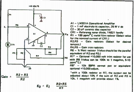
Fig. 13-17. Voltage reference standard schematic.
A1 - LM301A Operational Amplifier
C1 - 1 mF electrolytic capacitor, 25 WV dc
C2 - 30 pF ceramic disc capacitor CR1 - Reference zener diode. 1N821 family e R1 - 100 ppri/PC metal film resistor ( Select value for the nominal current of CRI.) R2,R3 - Gain resistors ( Select for desired tempco.) FM,R5 - Gain trim resistors R6 - % Watt resistor ( Value should be the parallel equivalent of R2 and R3.) R7• - Optional + 10.000 volt trim resistor for use with R8 ( Value can be 100k to 1 megohm, 5-10 ppm/C.) Re - 10k 89PR cermet pot or equivalent optional + 10.000 adjust.
with a 100k resistor at R7, the output can be adjusted about 10% if the sum of R2 and R3 is 10k. 1 megohm will provide about 1%.
---------------------
Versatile Power Distribution System
How many times have you entertained the thought of constructing an AC receptacle that will be portable on your bench and at the same time have some fuse protection for equipment under repair or construction.
Another nagging workbench item is the soldering iron. It would be difficult to determine how many times it sits on the bench of hobbyists cooking for days, or how many times experimenters accidentally burned themselves or damaged material lying on the workbench.
You can now have a portable switched three outlet AC power source with two of the outlets fused directional control light source, soldering iron power source with high/low heat and removable heat shield stand for the soldering iron.
This is another junk box project from start to finish. Selection of components is not critical as long as they can handle 115 volts at 5 to 9 amps.
In addition to the basic tools a small punch set and nibbler are needed. If you don't have access for borrowing one, Lafayette Radio usually has them in stock at a modest price.
Figure 13-18 is schematic circuitry of the magic box. A neon indicator light is always on as long as the box is plugged in. The indicator lights for outlets 2 and 3 are wired behind the fuses to indicate when a fuse is blown. If the builder is working with very low current fuses, the indicator light load should be placed in front of the fuse so as not to increase the current drain at the outlet.
Use an aluminum case 3" x 5" x 2". Try to place all the wiring in the lower half to simplify construction. The cradle microswitch support can actually be made from the frame of a broken rocker switch, if you happen to have one in your junk box.
The soldering iron cradle can be constructed from sheet aluminum. The microswitch is operated by a plunger-type rear support. A standoff spacer with a bolt for plunger will work well. The plunger should be designed with W' travel, allowing plenty of movement to insure switch operation and still protect from excess weight being placed on the cradle.
The light source can be an old desk lamp fixture. Placement of the light should allow free access of the soldering iron for right- and left-handed users. A high intensity light unit would make a better light source.
Parts placement is not critical.
With a little effort, your magic box can be made to look store-bought.
Remove all dirt and grease from aluminum and use a good primer base.
Aerosol lacquer spray paint is easily found in auto supply houses and hardware stores. Painting and labeling should be done before component assembly. Allow a day or two after painting for finish to reach maximum set.
Don't let the simple wiring circuitry mislead you into not checking before attaching to AC line.
Unique Power Supply Tester This supply tester uses a load bank. The first question asked might be "What is a load bank?" The term is taken from the electrical power industry...
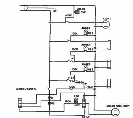
Fig. 13-18. Schematic circuitry.
...to explain a device to simulate a load on various power sources in order to check the load performance of those sources. This project covers the building of two simple load banks or dummy loads for small and rather large sized DC power supplies that are finding present usage with experimenters and hobbyists. It can be done economically and with readily available parts.
Also, using the basic ideas presented here, load banks for almost any type of low voltage power supply can be built.
In order to properly evaluate the performance of a power supply (whether home built or commercially built), the supply must be tested at various degrees of loading-that is, no load, half load, full load, etc. The major requirement for a suitable load bank is that it be capable of providing these various load conditions. Thus, several load elements are required, or at least one large variable element is required, in order to cover several different load conditions. These load elements would typically be large fixed or variable power resistors. If the power supply is of any size, the load elements have to be of high power rating ( 10, 25 or even 50 watt). A look at a parts catalog will show that power resistors get expensive as the power rating goes up and the different ohmic values available go down. Also, power resistors present the problem of how to get rid of the heat and how to conveniently mount the resistors.
Instead of using the regular power resistor in the design of these load banks, automotive bulbs and pilot lamps were used. These are readily available at auto parts houses and even department store electrical parts sections. Bulbs are selected on the basis of voltage and current requirements and typically work out very nicely in regard to both values. The problem of power dissipation is very minimal and mounting can be very simple. With the load elements decided, the actual construction of the load bank can begin.
The first load bank requirement was for a rather large 13.8 volt DC 24 amp DC supply. It was decided to check one third, two thirds, full load and 133 percent of full load. Voltage and ripple were observed under the various load conditions. The #1073 automotive bulb was selected with a nominal rating of 12.8 volts @ 1.8 amps. Typical cost is less than 30 cents. Since the power supply voltage was to be a volt higher, the current at that voltage was approximated to be about 2 amps. This is a fine feature of these bulbs-the voltage can be increased up to 20 percent of nominal rating without any problem in this application.
The bulbs were arranged in four groups or sections of four each. Each group presents a load of about 8 amps at nominal voltage to simulate four load conditions. In order to keep costs down and construction simple, the wires consisting of # 14 TW wire were soldered directly to the bulb bases.
The start and end of each section wire were wrapped around a nail which was driven into the wooden base board. This eliminated expensive sockets and, after all, a load bank is not a device that is normally on display in the shack.
Since this load bank was to be used for a considerable amount of testing and since four surplus relays were available, each load section was wired through relay contacts as shown in the diagram. Any combination of loading can be quickly selected. This extra feature can be eliminated with just the use of solder connections or switches with proper current rating. The switching feature is certainly handy if considerable testing is to be done, but adds considerably to the parts cost if the junk box is not well stocked.
The second load bank was for a much smaller DC power supply with a rating of 5 volts@ 1 amp. Following the same design features of the previous load bank, a #592 bulb was selected as load element in four sections with two bulbs in each section, giving 30 percent, 60 percent, 90 percent and 120 percent of full load. Since the current requirements were much less, about 0.3 amps per section, regular #22 solid hookup wire was directly soldered to the bulb bases and toggle switches (or even slide switches) used for controlling the load sections. A small wood base board was again used for mounting the bulbs and wiring with a small 1/2" pressed board panel (nailed to the edge) to support the switches. This supply is most useful for checking logic power supplies used with ICs. Overload or current foldover characteristics can be checked on supplies designed with that feature.
There are many advantages to these simple load banks besides the cost and ease of construction. The bulbs present a large amount of light under full load to leave no doubt that the supply is working. Also, there are no burn marks from power resistors on the workbench or, even worse, the dining room table. Buying the bulbs by the box reduces cost and automotive type bulbs are readily available, even at gas stations.
The purists may argue that the bulb is not a constant load resistance due to the filament characteristics. This sudden heavier than normal load when voltage is first applied to the bulb is very short in duration and provides an even stricter load test of the supply being tested.
The load bank ideas presented here can be extended to other sizes and types of load banks by changing the bulb types and the number of bulbs in a section, and even the number of load sections.
These load banks have been used to check voltage and ripple conditions on a variety of home brew and commercial supplies. The cost is certainly cheap if proper shopping around is done on the choice and source of bulbs.
The Smoke Tester Power Supply Checker Outer
This tester allows full power (smoke) testing of large or small power supplies before they are put on the rig. It will tell how many volts at how many amps the supply can deliver and what kind of voltage loss to expect under load. It can also help determine some of the attributes of low voltage power transformers, without having to wire them into a power supply.
It consists of two or three transistors, a pot, a couple of meters, a few diodes and some loose hardware. Don't forget the heat sink. If you wish to be formal about it, then add a chassis of some kind.
As the wiper is moved toward the plus, more current flows in the base circuit. The external circuit looking into the collector/emitter sees a lower and lower resistance. The ammeter and voltmeter give an idea of watts cooking. The diode allows less than perfect attention to the polarity of the incoming voltage. The resistor in series with the base limits base current to a safe value.
Although the transistor manual indicates that the 2N3055 is a "15 ampere" transistor, two or three of them cleared like fuses when the collector current was slowly increased above about 11 or 12 amps. The 10 amp fuse was put in the emitter, and collector current excursions were limited after that.
Since power supplies capable of giving more than 20 amps were to be tested, two 2N3055s were put in parallel. The fuses gave enough resistance in the emitters to help the transistors share the current in a more or less equal manner (at least there were no more creamed transistors). A Darlington or piggyback configuration is used to reduce the power dissipation requirements of the pot. Ten amps in the collector can require as much as 1/2 amp in the base. Half an amp times several volts equals several watts. The Darlington system reduces the input current by as much as 50 times. That figures out to about 10-20 mA for 10-20 amps in the collectors, and makes the system practical.
Note that if the power supply is delivering 15 amps at 13 volts, then something is going to have to dissipate 195 watts. Be sure that the 2N3055s are on a large enough heat sink.
If a full wave bridge rectifier is placed in front of the tester, power transformers can be checked for voltage out versus current. That information would have saved a lot of time in the past.
Of course, there are single transistors around that meet the voltage, current and power ratings of this tester.
If PNP transistors are used, reverse the polarity of the meters and diodes.
--
Prev: RF Test Equipment