Ultra Simple Diode Checker
This simple diode checker is an up-to-date version of an idea that has been around for a number of years. It can be built in one or two evenings from the parts in most experimenter's junk boxes. The parts required are one resistor, two LEDs, and any 117v AC transformer that will provide from 3 to 25v AC. Discarded audio interstage transformers from old tube-type radios and TVs can be used. If all new parts are bought, the cost will be about $5.00, including the small aluminum box. The small cost can be recovered many times over by buying unmarked, untested, manufacturer's closeouts, diodes by the pound, etc., available from most discount mail-order houses (like Poly Paks). Bad diodes can cause disastrous results in some circuits and can be difficult to detect and locate in other circuits. It is a wise precaution to check them all before installation. This simple diode checker was conceived and built for just such purposes.
The Circuit. The simple schematic is shown in Fig. 6-1. The trans former provides a low AC voltage, through the current limiting resistor, to two LEDs connected back-to-back. The diode to be tested is connected in series with this combination and the return side of the transformer. The LEDs will respond to the four possible conditions of the diode under test. If the diode is open, no current flows and neither LED will light. If the diode is shorted, one half cycle of the AC voltage will light LED1 and the other half cycle will light LED2. Since each LED is lit 60 times per second, a shorted diode will cause both LEDs to appear lit continuously, ff the diode is good, LED1 will light when the diode's anode is toward the return side of the transformer and LED2 will light when the diode's cathode is toward the transformer return side. By proper physical arrangement of the LEDs and diode, the LED near the diode's cathode will always light.
The resistor should be sized to limit the current through the LEDs to about 10 mA. Most LEDs will have a voltage drop of about 1.5 volts across them and most signal-type diodes will have from 0.1 (germanium) to 0.5 (silicon) volts drop across them. The resistor value can then be found by subtracting these two voltages (say 1.5 and 0.5) from the transformer voltage and dividing by 10 mA: VXFMR - 1.5 - 0.5 R - 0.010
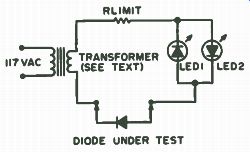
Fig. 6-1. Schematic.
For a 6.3v AC transformer, the resistor value is 430 ohms. A 330 or 470 ohm resistor will do. Its value is not critical.
Construction. The simple circuit lends itself well to point-to-point wiring, which is probably the quickest way to build the checker. If the builder prefers a neater appearance, the printed circuit board layout shown in Fig. 6-2 can be used. It is easy to duplicate with an etch-resist pen, or, if a professional look is desired, by photographic means. Figure 6-3 shows the parts placement for the circuit board and Fig. 6-4 shows the matching hole locations for mounting it in a 4 x 2-1/8 x 1-5/8 box. A Radio Shack 6.3 volt transformer, stock number 273-1384, was used for the circuit board layout and hole patterns. No on/off switch is used. The unit is simply plugged in for use. A TV cheater cord plug and socket are used so that the diode checker is easy to store without dangling AC cords everywhere.
Pin jacks, banana jacks or five-way binding posts can be used for connecting to the diode to be tested. The binding posts allow for a variety of connections to diodes that cannot be brought directly to the checker.
Adapters with a V-notch are used so that loose diodes can easily be dropped into place for testing. Figure 6-5 shows two easy methods of making such adapters.
Fig. 6-2. PC board layout.
The holes should be cut in the box, and it should be painted and labeled to suit the builder's taste. The current limiting resistor and transformer should be mounted to the circuit board next. The AC plug and pin or banana jacks should then be mounted in the box, with short lengths of wire soldered to them. Next, insert the LEDs and bend their leads so that they will not fall out. Do not solder them yet. The LED leads must be long enough for the LEDs to protrude through the box, so the builder may have to add short lengths of wire. Now feed the four wires from the AC plug and the jacks through the proper holes in the circuit board, check for proper fit and clearance and solder the four wires. Position the LEDs and solder them to the circuit board. Put insulation on the inside of the box bottom to prevent any possibility of shorts to the circuit board. Don't forget that it has 117v AC on it! Make adapters to fit your jacks and you are ready to check out the unit.
Test the checker by applying power to the 117v AC plug. Neither LED should light. Now put a short circuit across the jack terminals and both LEDs should light. A diode that is known to be good should now be connected across the jack terminals. The LED closest to the diode's cathode should light. Try it both ways to make sure the LEDs are oriented properly.
After building and using this simple diode checker, the owner will find a desire to also know, if the diode under test is silicon or germanium. Since a germanium diode will develop about 0.1 volts across itself and a silicon diode about 0.5 volts, it seems that some very simple circuit might be devised that would light an LED if the diode under test were silicon.
The Amazing Zener Sweeper Tests Zener Diodes
Have you ever acquired a packet of unmarked, untested zener diodes from one of the surplus dealers? Perhaps you have discovered that sorting and testing 100 such zener diodes is a rather formidable task.
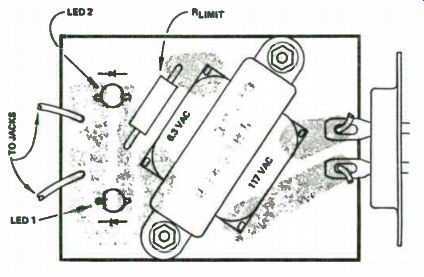
Fig. 6-3. Parts placement drawing.
The common method of testing a zener diode is by connecting the zener in series with a limiting resistor across a variable voltage source and metering the zener voltage (Fig. 6-6A). As the supply voltage is increased, the voltage across the zener diode will be equal to the supply voltage until the zener point is reached. At that point, the voltage across the zener will cease to rise with further increase in the supply voltage, and the meter will indicate the zener voltage. This test, however, does not make it readily apparent whether or not the zener under test is leaky. In Fig. 6-6B, this zener diode leakage is represented by RZ in parallel with the diode. The applied voltage will divide across RL and RZ until the zener point is reached, at which time it will stabilize. In this case, the voltage across the zener diode increased with increasing supply voltage, as it should, but it was less than the supply voltage.
The shortcomings of this method can be overcome by using a sawtooth test voltage and monitoring the zener voltage with an oscilloscope whose horizontal sweep is driven by that sawtooth. This is possible with an oscilloscope that provides front-panel access to its internally-generated sweep voltage, as shown in Fig. 6-7. The displayed ramp will rise to the zener point, beyond which it will be a horizontal line. If the zener passes current before the zener point is reached ( is leaky), the ramp will be curved.
If the zener does not go into complete conduction at its zener point (is resistive), the horizontal trace will continue to rise. This would seem the ideal method, but it does have several disadvantages:
• Not all oscilloscopes provide front-panel access to the sweep voltage.
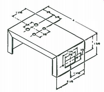
Fig. 6-4. Hole pattern for a 4 x 2-1/8 x 1-5/8 inch box. Cut holes to fit
parts on hand. Holes are centered on centerline of box.
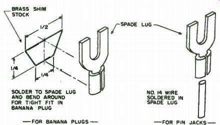
Fig. 6-5. Adapters.
• The trace on the screen often begins after the voltage on the sweep output terminals has risen to some value, making it impossible to test zeners of voltages lower than that value.
• It is somewhat time-consuming for use in testing any great number of devices. (Remember that packet of 100 unmarked, untested zeners?) Perhaps you have anticipated the next step. A sawtooth generator whose output has a zero baseline and sufficient amplitude to exceed the voltage of the zeners to be tested will do nicely. Described hereafter is a tester that provides these features. The circuits, far from original, have been borrowed from various sources and modified as necessary to utilize the contents of a junk box.
Figure 6-8 is a block diagram of the tester. A sawtooth, controlled by a multivibrator, is amplified and applied to the test circuit. Jacks are provided for connections to the oscilloscope inputs and for leads to connect to the zener under test.
The heart of the tester is an integrator with a clamping transistor to reset the timing capacitor at the end of its timing cycle, which produces a ...
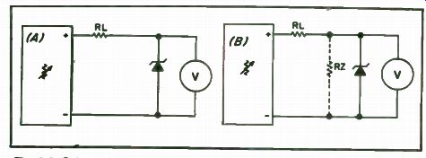
Fig. 6-6. Schematic.
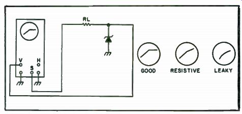
Fig. 6-7. Schematic.
... sawtooth (Fig. 6-9). The required control voltage, EC, is obtained from an astable multivibrator. When EC is high, D9 is reverse biased and the positive voltage, applied through R8, holds Q3 in saturation. R12 is thus in parallel with C7, the timing capacitor. E0 is then essentially zero. When EC goes low, D9 conducts and D10 and D11 are reverse biased. Q3 turns off and the circuit begins to integrate at the rate of I R10 x C7 volts per second.
This rise continues until the control voltage again goes high, driving Q3 to saturation and discharging C7. With the components shown, the rise is approximately 560 volts per second. The amplitude of the ramp produced is dependent on the timing rate, limited by the voltage applied to the integrated circuit.
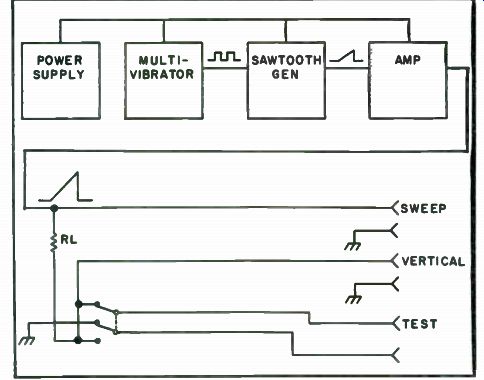
Fig. 6-8. Schematic.
Figure 6-10 shows the astable multivibrator that produces the control voltage. The timing components are C5, R5 and C6, R6. The time interval of conduction of the transistors is given by: T = 0.692 x C x R. With the components shown, pulses of approximately 7 milliseconds duration are obtained with an amplitude of 18 volts. This is quite adequate to control the sawtooth generator.
The sawtooth from IC1, approximately 4 volts in amplitude and of 7 milliseconds duration, is applied to a two-stage direct-coupled amplifier (Fig. 6-11). Output from the amplifier section is a 40-volt sawtooth whose duration is somewhat less than 7 milliseconds, having lost a bit due to the bias on transistors Q4 and Q5. Q5, a GE152, is the only critical component in the tester. It must have good linearity, low leakage and an adequate voltage rating.
The power supply (Fig. 6-12) is designed to provide both positive and negative 6 volts from a single low-voltage secondary. A bridge rectifier is connected with equal loads on its positive and negative outputs. Equal current flows in both loads; hence, equal voltages of opposite polarity are developed. These power the LM741. The high-voltage secondary provides +40 volts for the output amplifier, which ensures that the test sawtooth will be sufficient amplitude for the range of zener diodes normally encountered in the shop where this tester is in use. R3 is used to drop the +40 volts to +20 volts to power the multivibrator.
The zener diode tester is quite simple to use. Connections are made from the tester to the vertical and horizontal inputs of an oscilloscope whose vertical amplifier is set for DC and whose horizontal amplifier is set for external. The zener diode is connected to the test terminals and a graphic representation of the zener characteristics is displayed on the oscilloscope screen (Fig. 6-13). The zener voltage may be read on the screen if the oscilloscope is calibrated. A polarity-reversing switch is provided for convenience in switching the polarities of the test terminals. A normal zener will produce a distinctive trace, while a defective device will be readily apparent (Figs. 6-14 and 6-15), thus facilitating rapid testing. Figures 6-16 and 6-17 show the layout used in the prototype of this tester. Nothing in the layout is critical, which means a great deal of variation is possible, so you can make use of any available parts.
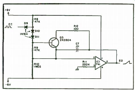
Fig. 6-9. Schematic.
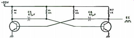
Fig. 6-10. Schematic.
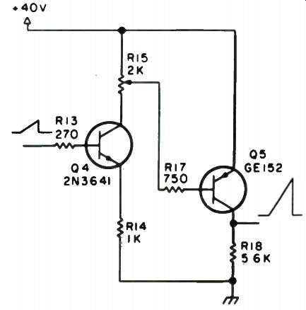
Fig. 6-11. Schematic.
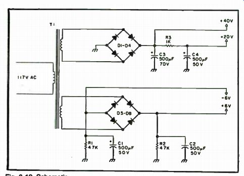
Fig. 6-12. Schematic.
Though constructed only recently, this tester already has proven to be of tremendous value. Several previously inexplicable power supply problems have been resolved by demonstrating that a zener knee was not sharp.
Additionally, more than 100 unmarked, untested zener diodes, purchased from a surplus dealer has been tested and sorted.
Presto Transistor Checker from VOM
Vacuum tubes and transistors have to be tested in special testers, usually in the shop or lab, to determine their condition or defect. This still holds true for vacuum tubes but, because the transistor has advanced so rapidly and become so popular in the electronic field, it has been difficult to test.
Many good transistor testers have been designed. But, they still require that they be used in the shop or lab. They may even be tested on an oscilloscope for performance to determine their operative ability or leakage condition.
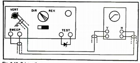
Fig. 6-13. Schematic.
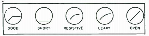
Fig. 6-14. Reactions of tester.
The Multimeter Test Meter, Simpson or Triplet type, has become the technician's and serviceman's most handy and important tool for servicing on the spot today. This Simpson test meter made possible the fast checking of tube circuits and other electronic parts on the spot on complex systems and important electrical and electronic devices. Today this same meter is being used on the new state-of-the-art printed circuit cards, solid state circuitry, transistors, diodes, etc.
This adapter/conversion board makes possible the simple change over of a common test instrument (Simpson or Triplet) into a transistor tester for on the spot testing of normal defects of transistors, diodes or other solid state devices. For a complete parts list, see Table 6-1.
Using the standard Simpson 260 meter, a printed circuit card adapter, with a circuit for testing general type NPN and PNP transistors and solid state components for defects, is "piggy-back, plugged-in" over the existing controls on the meter. The settings are then set to 50µA and DC on the meter controls. This results in now having a full transistor tester with new controls on the printed circuit adapter (Fig. 6-18). Connect the PC board to the meter by way of the mounting banana male studs. This makes the necessary connection to the Simpson 50 microammeter direct. Add the clip-on battery, to complete the conversion of the ...
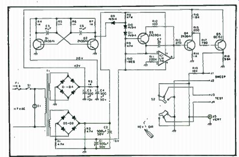
Fig. 6-15. Zener diode tester.
Fig. 6-16. Panel layout.
... multimeter to a transistor tester. The controls on the adapter enable the operator to adjust the 50 micro-ammeter for full scale. Or, scale 1.
This full scale of 1 can be used for the gain measurement of DC or alpha, which is less than unity. By using the selector switch on the adapter board, you can check the DC gain-Iceo, -Icbo, lebo-the last three being diode action, reverse current and action test for front-back leakage. This takes
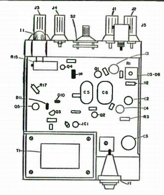
Fig. 6-17. Component location.
-------------
Table 6-1. Parts List.
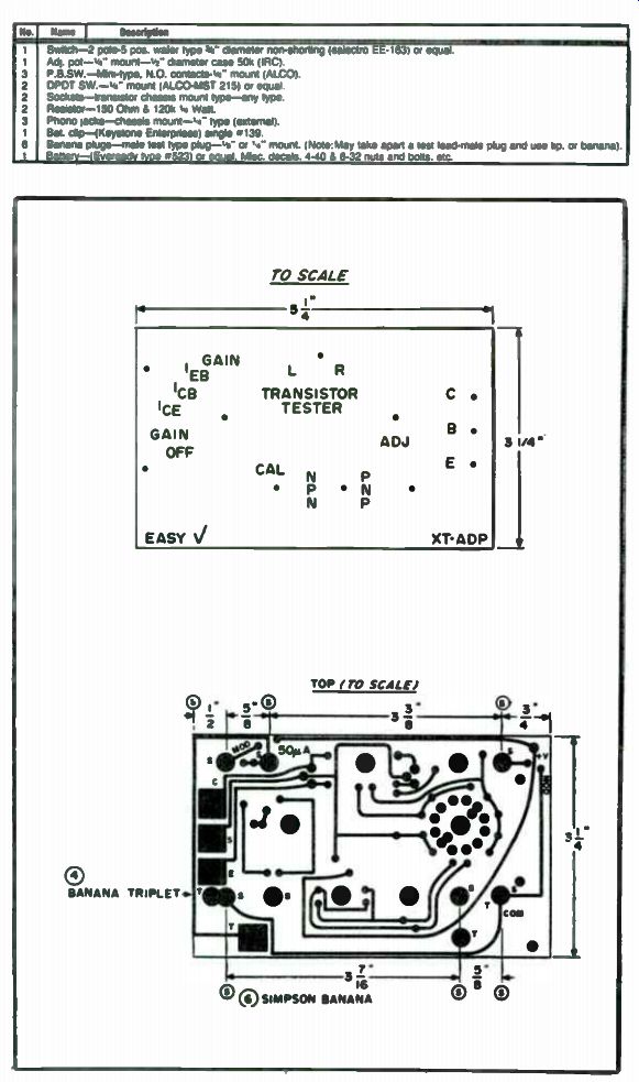
Fig. 6-18. Schematic.
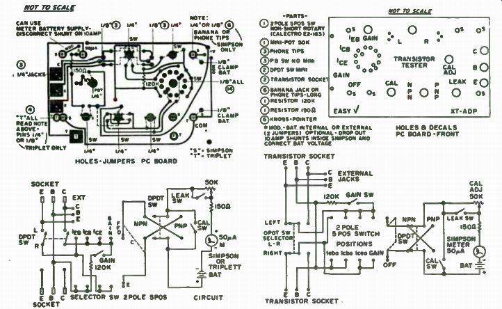
Fig. 6-19. Transistor adapter circuit for Simpson 260.
... care of the leakage currents in the base, emitter and collector, and makes a quick gain check on the tested transistor.
For diodes, external pin connections "C and E" and left position on the selector, make this check possible. Transistor comparison testing is made possible with the "L and R" selector switch. Leakage switch is used to making the 50 microammeter more sensitive for lower leakage readings.
This tester adapter can be hand wired on a small board and adapted to other meters. This PC board has been designed for either the Simpson 260 or 270 and the Triplet 630 series. Mounting and drilling holes for the two types are marked as "S" and "T" Fig. 6-19. The board is called EASY XT-ADP.
Test Those ICs
There is a definite need for an integrated circuit tester with much greater flexibility and capability than those commonly found in current literature or available commercially within reasonable cost.
Many IC testers which have been described recently are designed to use either a dedicated IC socket for each IC tested, or some form of hardware programming device to interconnect Vcc, GND, logic in, logic out and other necessary control signals. Other types of testers commercially available employ multiple-pole slide or rotary switches for programming.
Although both approaches are satisfactory for testing a limited number of elementary gates, counters and flip-flops, the cost to dedicate the very large number of IC sockets or other hardware programming devices necessary to test a great variety of chips generally has been considered too prohibitive; as a result, the testers previously described have a limited number of ICs they can test.
The IC tester described here is capable of testing a very wide range of DTL, TTL and CMOS digital logic functions, including single and multiple input gates, inverters and buffers, flip-flops, counters, shift registers, latches, one-shots, pulse synchronizers, multiplexers/encoders, demultiplexers/decoders, arithmetic logic functions, switch de-bouncers, priority encoders, true/complement elements, parity generators and many others. Specific TTL and CMOS ICs which are testable are listed in Table 6-2. Others may be added to the list, but have not been investigated.
Design Considerations. The primary objective of this project was to design a quality tester which maximizes the number and types of digital ICs testable and to do so with minimum cost. Other design goals achieved were:
• Unit can act as an in-circuit, logic-state monitor
• Tester tests over 450 different TTL digital ICs
• Tests CMOS digital ICs (directly compatible)
• Tests 7400, 74H00, 74L00, 74LS00 and 74S00 series
• Tests open-collector and totem-pole output TTL ICs
• Full CMOS input gate protection
• Internal three speed clock
• Vcc applied before any logic signals applied
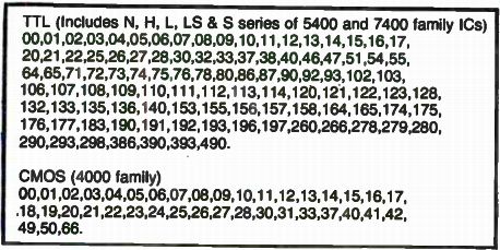
Table 6-2. ICs Known to be Testable.
• Icc monitor provided
• Rapid, easy programming
• Tests both 14- and 16-pin dual in-line packages
• Six separate logic input and six separate logic output lines
• Rapidly tests many ICs of same type by using IC clip
• Each logic output line monitored independently
• Built-in 110v AC power supply
• +9v or + 12v DC input capability for portability
• Convenient size, attractive case
The above features, and the logical design of the IC tester circuit, were arrived at by seriously examining the required parameters to be tested on the various IC chips. Two basic categories of parameters are normally specified for digital ICs -dynamic and static. Table 6-3 summarizes the basic differences between static and dynamic testing.
Dynamic parameters of digital logic chips include gate propagation delay, maximum clock toggling frequency, output rise and fall times and other properties designed into the chip which specify input and output conditions at very high clock input rates. Basically, dynamic testers deter mine how well the IC works.
Static parameters include the Vcc and ¡cc required and the fundamental ability of the logic chip outputs to correctly follow the various logic inputs for that chip, according to its respective truth table, i.e., "Does the chip work?" Since ICs are manufactured to stated minimum and maximum specifications (reflected in their dynamic and static operation parameters), there is a very good degree of assurance that the IC will function properly in a circuit, if its static operation is correct and it is not required to operate above its minimum guaranteed operating frequency or otherwise outside its specified dynamic operating characteristics. The great majority of applications for digital TTL or CMOS ICs do not require near-maximum performance of the chip (except, perhaps, for VHF or UHF prescalers and gigabit logic applications, where ECL or other newer technologies are used). Therefore, a static tester will be quite adequate since, if the chip does work correctly, it can be expected to meet at least its minimum dynamic operating characteristics in a particular design application.
Since it is terribly frustrating and time-consuming to either debug a logic circuit prior to getting it working or troubleshoot the circuit to find out why it has stopped working, a few simple quality-control procedures taken before installing the IC can save many headaches later. The easy-to-perform burn-in process, described later, followed by static testing with the tester detailed, will give you a very high measure of confidence that the ICs you use are good when you install them and that they will remain in working condition for many, many years, if not subsequently damaged electrically or physically.
Circuit Description. The function block diagram for the IC tester is shown in Fig. 6-20. Each pin of the device under test (DUT) is interconnected by the switching matrix, as required for the particular IC tested, to +Vcc, GND, up to six logic input and six logic output lines, as well as four other signal lines. One side of the matrix has a line for each of the 16 pins and the other matrix side connects to the input and output circuits and controls.
Many switch matrix alternatives were evaluated in terms of cost, physical size and switch capacity required. The 20 x 20 pin-plug matrix board was discarded as both too bulky and costly. A programmable solid state switching array was found to be possible, but not practical, in terms of components and supply current required. A miniature jack and jumper pin matrix suffers the same problems as the plug-pin matrix and, additionally, introduces the requirement to store many jumper wires. Matrix cost and size were minimized by using an array of twelve 16-pin DIP switches, each containing eight SPST rocker switches. However, with only 96 switches available, they must be utilized to the very best advantage to interconnect the inputs and outputs of those ICs most likely to be tested.
The particular matrix organization shown in Fig. 6-21, was painstakingly selected to allow the maximum number of ICs to be tested with a convenient number of DIP switches. If desired, additional DIP switches can be added to increase the number of matrix cross-points interconnected, consistent with the panel space available. Although it is apparent that many matrix cross-points are not provided an interconnection by one of the switches, with only a very few exceptions, all input and output logic lines for the ICs listed in Table 6-2 are testable with this matrix arrangement. For those ICs having more than six input or output lines (e.g., an eight-bit multiplexer), the DIP switch matrix can easily be reprogrammed to test those logic lines not tested with a single DIP switch setup.
Input logic signals to the DUT are generated by depressing the correct combination of push-button switches, in conformance with the logic input requirements specified in the truth table-up=logic 1, down = logic 0. In addition, an internal clock can be supplied as a logic input signal for input
#1, and fed through the switch matrix to the selected input pin of the DUT. Three clock speeds have been incorporated-a slow speed (1 Hz) for monitoring latching operating, a medium speed (3 Hz) for toggling most gates and a high speed ( 10 Hz) for clocking multibit counters, shift registers, etc.
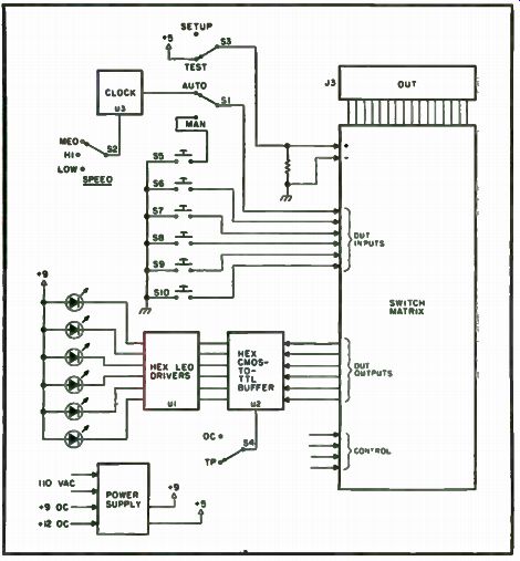
Fig. 6-20. IC tester functional block diagram.
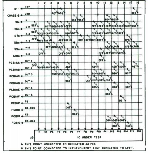
Fig. 6-21. DIP switch matrix.
The +5 Vcc (Vcc and Vdd for CMOS), GND and other input signals lines are also connected to the proper pins of the DUT, via the switch matrix. Monostable multivibrators (e.g., 74121, 84122, 74123) require timing resistors and capacitors for proper operation. These are R23, C8, R24 and C9 in Fig. 6-22, and have been selected to give approximately a 1/2-1 second low-high-low indication at the respective output monitor.
Output logic states of the DUT are led from the switch matrix through a hex CMOS-to-TTL buffer to individual LED drivers for display. A high output logic level (logic 1) from the DUT lights the LED, and a low output logic level (logic 0) is indicated by an unlit LED. Unused output LED indicators remain unlit.
During setup, S4 is placed into either the OC or TP position, depending on whether the DUT is of the open-collector or totem-pole output variety.
This action connects or disconnects a pull-up resistor to each logic output pin of the DUT. The pull-up resistors are required only for open-collector ICs, since the output transistor collector is un-committed (Fig. 6-23) for high voltage or high-current applications, whereas the totem-pole output transistor collector is connected internally to another transistor (Fig. 6-24) to provide direct TTL output levels without the requirement for an external pull-up resistor.
----------------------
Table 6-3. Static and Dynamic Testing Comparison.
Type of testing Clock frequency Complexity Commercial cost Static testing Dynamic testing Functional Truth table compliance Icc ( quiescent drive current)
Low to medium Simple-switches and logic indicators
$500-$1000
Full parameter Propagation delay Max toggle frequency Noise immunity Min. clock pulse width Fan-out/Fan-in Near maximum rated Very high-normally special-purpose or custom-designed ROM or microprocessor-controlled
$1500 (benchtop) to over
$50,000 ( production line)
----------------------
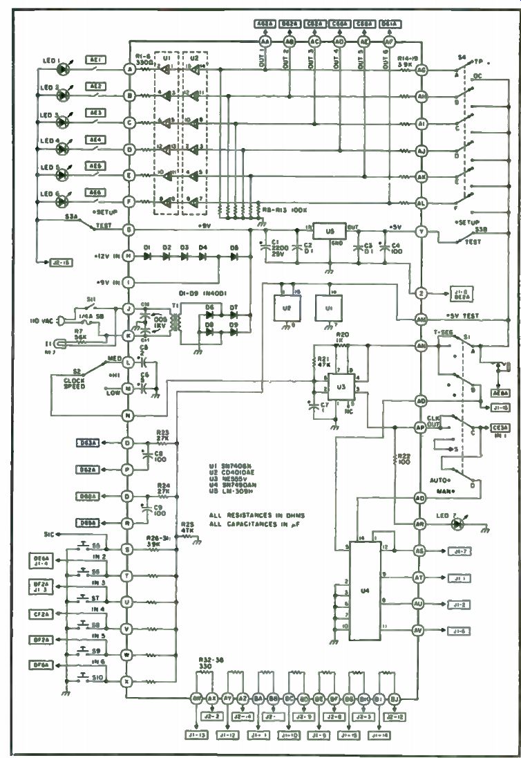
Fig. 6-22. Logic board ( PCB-1) schematic diagram. Connection points inside
rectangular boxes refer to external jacks (J1-6=pin 6 of jack J1) or PCB-2
switch matrix connection points ( DF6A=pin A of DIP switch DF 6). N.B Insulate
jack from chassis.
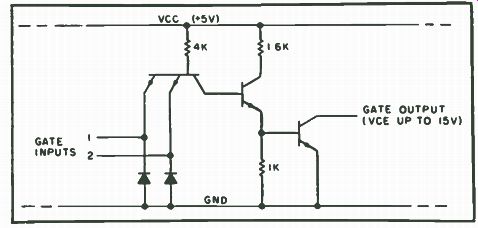
Fig. 6-23. Open-collector output gate ( 1/4 SN7438N).
Power Supply. A conventional full- wave rectifier bridge (D6-D9) and a +5v regulator (U5) are included to power all logic circuitry, as well as the DUT. A separate +9v + 12v DC input jack may be installed by those desiring complete portability. The external battery supply voltage is dropped to about +8 by D1-D4, to reduce the voltage drop across, and hence, the amount of heat dissipated by U5. The diodes also provide battery polarity protection. The +5v supply line powers the DUT and the tester circuitry only when S3 is in the TEST position. This prevents inadvertent application of input logic levels prior to application of Vcc to the DUT, since the input logic levels are themselves derived from the same +5v line. With S3 in the SETUP position, all input, output and Vcc lines to the DUT socket are returned to ground. An optional 0-100 milliammeter can be inserted in the Vcc line to the DUT to monitor the current required, or the Vcc line can be run to a closed-circuit three-way jack to permit external monitoring with your VOM. 7-Segment Decoder-Driver. Special provisions have been included on the logic printed circuit board to allow the popular SN7447A7-segment decoder-driver to be tested. The output pulse stream from U3 is fed to an internal dedicated BCD counter, U4, and the four binary output lines are led directly to Ji. Since this IC socket is dedicated for testing only the 7447A, the input and output lines required can be hardwired to J1 and J2. A common anode 7-segment display can be permanently installed at J2. When testing the 7447A, Si is set to 7-SEG and J1 is used as the test socket instead of J3.
U4, J1 and J2 are optional, but considered very useful to extend the tester's capabilities to the ubiquitous 7- segment decoder so popular in digital displays, counters, DVMs, etc. The internal BCD counter, which is hardwired to JI, allows the 7-segment display to cycle through all numerals 0-9 continuously. Additionally, the all segments on and all segments off tests can be performed on the 7447A under test.
Construction. The LMB 007-746 sloping panel cabinet was selected since it is both attractive and conforms to the physical layout requirements of the panel controls. The entire logic circuitry, shown in Fig. 6-22, including the power transformer, is implemented on a single PC board. The DIP switch matrix is on a second PC board. Thus, there are no components external to the PC boards except the required controls, LEDs jacks and switches. The switch matrix board (PCB-2) is wired (wire-wrap or point to-point) prior to installation, to reduce interconnection time required between it, the main logic board (PCB-1) and the panel controls. The use of IC ...
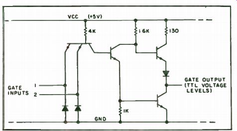
Fig. 6-24. Totem-pole output gate ( 1/4SN7400N).
... sockets on PCB-2 permits the DIP switches to be removed temporarily for other uses, if desired. PCB-1 is laid out to accept IC sockets for each IC, although the use of sockets is not mandatory. Ribbon cable is used to interconnect the PCBs and controls, although a combination of wire-wrap and point-to-point wiring can be used.
A significant measure of flexibility can be added to the tester by using an IC clip and ribbon cable which connects toJ3. This permits very rapid testing of many ICs of the same type and also greatly extends the lifetime of J3.
Either 14- or16-pin ICs can be tested directly, since the DIP switch matrix programming accounts for pinout differences as long as pin 1 of the IC clip lead (or J3) is always connected to pin 1 of the 14-or 16-pin DUT when testing.
Operation of the IC Tester. Due to the wide variety of IC functional pinouts, it is necessary to set up the DIP switch matrix to interconnect the input/output signal lines to the proper IC pins for each different functional pinout, but not necessarily for each different IC. For example, Fig. 6-25 and Table 6-4 show a sample truth table page, which can be used for testing many IC types. There are four related parts to each page-the listing of ICs testable by the matrix settings on that page, the matrix settings, the truth table and, for easy reference, the pinout configuration for each IC listed on that page. For a complete parts list for this project, see Table 6-5 and Figs. 6-26 and 6-31.
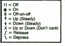
Table 6-4. Truth Table Notation.
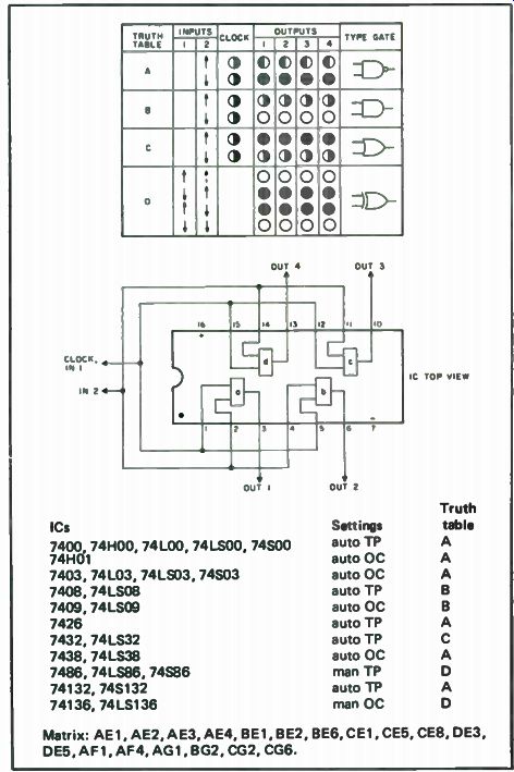
Fig. 6-25. Sample truth table. See Table 6-4 for explanation of notations.
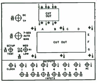
Fig. 6-26. Front panel.
--------------
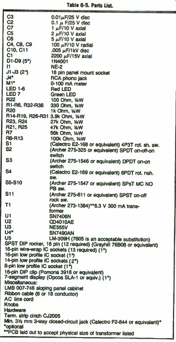
Table 6-5. Parts List. C3 0.01µF/25 V disc C2 0.1 µ F/25 V disc C7 1 µF/10 V axial C5 2 µF/10 V axial C6 5 µF/10 V axial
04, C8, 09 100 µF/10 V radial C10, C11 .005 µF/1kV disc C1 2200 µF/15V axial DI- D9 ( 5* 1N4001 11 NE-2 J1-J3 (2*) 16 pin panel mount socket J4* RCA phono jack M1* 0-100 mA meter LED 1-6 Red LED LED 7 Green LED R22 100 Ohm, 1/4W R1- R6, R32- R38 330 Ohm, 1/4 W R20 1k Ohm, 1/4W R14- R19, R26- R31 3.9k Ohm, 1/4W R23, R24 27k Ohm, 1/4W R21, R25 47k Ohm, 1/4 W R7 56k Ohm, 1/4W R8- R13 100k Ohm, 1/4 W Si (Calectro E2-168 or equivalent) 4P3T rot. sh. SW. S2 (Archer 275-325 or equivalent) SPDT on-off- on switch S3 (Archer 275-1546 or equivalent) DPDT on-on switch S4 (Calectro E2-169 or equivalent) 6PDT rot. nsh.
SW. S5-S10 (Archer 275-1547 or equivalent) SPsT MC NO PB sw.
Sil (Archer 275-611 or equivalent) SPST on-off rock sw.
T1 (Archer 273-1384)**6.3 V 300 mA trans former U1 SN7406N U2 CD4010AE U3 NE555V U4* SN7490AN U5 LM-309H ( 7805 is an acceptable substitution)
SPST DIP rocKer, 16 pin ( 12 required) ( Grayhill 76B08 or equivalent)
16-pin wire-wrap IC sockets ( 13 required) ( 1*) 16-pin low profile IC socket ( 1*) 14-pin low profile IC sockets ( 2') 8-pin low profile IC socket ( 1') 16-pin DIP clip ( Pomona 3916 or equivalent)
7-segment display ( Opcoa SLA-1 or equiv.) ( 1')
Miscellaneous LMB 007-746 sloping panel cabinet Ribbon cable (8 or 16 conductor)
AC line cord Knobs Hardware Term strip cinch CJ2005 Min. 3l/2 min 3-way closed-circuit jack ( Calectro F2-844 or equivalent)
*optional
*PCB laid out to accept physical size of transformer listed
------------------
To test an IC (e. g. , SN74LS08N), the switch matrix and other required panel controls should be properly set before inserting the DUT into J3. S3 is first put into the SETUP position, S4 is set to either OC or TP and the DIP switch matrix is programmed. S3 is then placed to TEST and the operations called for in the input portion of the truth table are then performed. Each gate output is monitored separately on (in this case) output LED indicators 1-4. If three outputs agree with the truth tables and the fourth does not, the pinout diagram will tell you how that gate is being tested by which inputs.
You may want to remove the pins to and from the defective gate and use the three functional gates later in another application.
To prevent the possibility of damage to the IC under test, return S3 to the SETUP position prior to removing the IC from the test socket or IC clip.
No other precautions are necessary to use the tester for CMOS or TTL ICs, except for proper IC handling procedures and ensuring that pin 1 of the IC is always connected to pin 1 of J3.
A very flexible property of this IC tester is that, if equipped with the ribbon cable and IC clip, in-circuit monitoring of up to six logic lines of an operating IC can be done. The only precaution necessary for this type of operation are to ensure a common ground between the IC tester and monitored IC, input lines from the tester (by opening the appropriate DIP switches in the matrix) and to place S4 in the TP position. The six output LED monitors, however, can be connected, as desired, by the DIP switch matrix to monitor either input or output lines on the IC. The IC tester uses a CMOS-to-TTL hex buffer in the output monitoring circuit; therefore, loading of the monitored IC, whether TTL or CMOS, is not a problem since the typical buffer gate input current of 10 pA is low enough to not alter the fan-out of the monitored IC. IN-QC (Quality Control). The procedures just outlined will test an IC to determine if it is working now, but cannot guarantee that the IC will not fail 10 minutes from now. Digital ICs are fairly well standardized and spot sample tested prior to shipment by most manufacturers. However, even in prime quality lots, a certain percentage may be found which are initially defective or which are prone to failure during the infant mortality period of use (first 48 hours under power). The percentage defective may vary widely between IC types of the same family; for instance, combined initial and infant mortality has been found to be as low as 1 in 200 for the SN7400N and as high as 1 in 15 for the SN7473N for the prime quality lots tested.
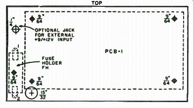
Fig. 6-27. Rear panel.
In order to ensure that the ICs used in your projects are good, and will remain good for many years, the easy bake-in and testing sequences which follow are strongly recommended, particularly if IC sockets are not used in your projects. These procedures, while not absolutely fool proof, can identify up to 95 percent of the faulty or fault-prone ICs for 90 percent of the common failure modes. ICs passing these tests have a very high probability of a useful lifetime in excess of 20 years, if not subsequently subjected to undue electrical or physical stress.
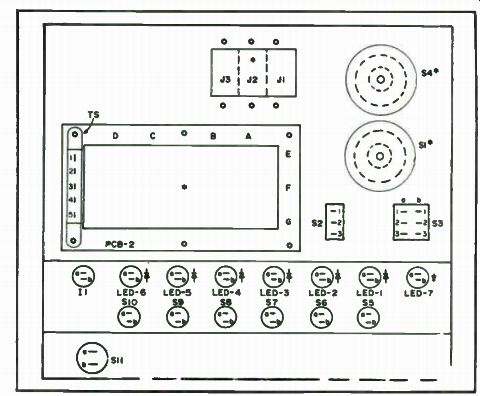
Fig. 6-28. Front panel interior parts placement. See Fig. 10.
The procedure is accomplished by temperature stressing the IC and then testing its static operation in the tester described. Place the ICs to be tested on a cookie sheet and bake at 250°F ( 120°C). Remove and place in
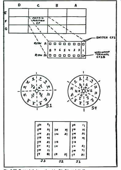
Fig. 6-29. Expanded views of matrix, S1, S4, and J1-J3.
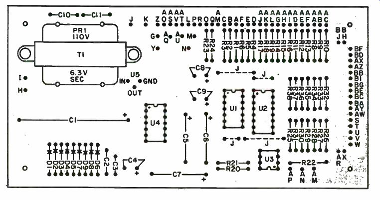
Fig. 6-30. P013-1 parts placement.
... the coldest freezer you have for 15 minutes. Re-bake and refreeze a second, third and fourth time. Finally, bake the ICs at 250°F for 48 hours. After they cool, visually inspect each for casing cracks and test them on the tester.
Experience has shown that only about 1-2 percent of the ICs that tested good before the baking process failed the post-bake-in testing. These were the failure-prone ICs, which probably would have failed later in the operating circuit and required troubleshooting of the circuit.
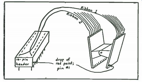
Fig. 6-31. DIP clip ribbon cable connections.
How to Find a Forgetful Computer Memory
Simple memory diagnostic programs for 8080-based systems have been described and illustrated for its use in troubleshooting 4K memory boards. While those methods are effective for localizing gross defects, such as chips which have one or more bits permanently set, more subtle defects may evade detection. For example, after discovering four bad chips in 8K of memory an attempt was made to load and run SCELBAL--but to no avail.
After many hours of checking and reloading scattered addresses with the correct contents, it dawned on the programmer that when the contents of some addresses were corrected, the contents of other addresses were sometimes changing. What obviously was needed was a more thorough memory debugging approach. This project brings us one step closer to that end and SCELBAL is now running fine.
Two basic techniques are employed. One technique takes the value of an address and loads it as a data word into that same address. This is done for all of the 256 addresses on a page. Next, the values of the addresses are compared with their respective contents. If they are dissimilar, an error printout is produced. For example, if the eighth data bit (bit 7) at address 023 is always set to 1 due to a chip defect, the actual contents of that address will be 223, which would generate an error. However, if bit 0 of address 023 was always set to 1, no error would be detected. Needless to say, this would cause problems in an actual program which required that bit 0 at address 023 be set to O0. One way that this problem can be overcome is to use a slightly different approach. Typically, this second technique loads a random number into all 1/4 K addresses of a page and then sequentially examines the contents of the 256 addresses to see if they still contain the pattern which was loaded into them. If enough random patterns are tried, a bit at some given address which is permanently set will sooner or later be discovered. However, a not uncommon problem is for two or more addresses to interact. If addresses 023 and 025 were interacting in such a manner that whatever was loaded into bit 7 at address 025 changed the corresponding bit in address 023, then this second technique would not detect the error by virtue of the fact that the whole page was loaded with the identical data word.
As if this isn't trouble enough, programs which check only one page of 256 addresses at a time are unable to detect interactions between two or more of the four blocks of 256 bits which actually reside on a single 2101 type memory chip.
This program overcomes the shortcomings just listed. When fully implemented, it provides a potent tool for detecting memory problems.
About the Program. In this system, the program, which is listed in Table 6-6 resides on page 043, address 200-320 (octal). Relocation should provide little difficulty once the mechanics of the program are understood.
The program loads a Test Word (TW), either 377 or 000 (octal), into one address in a 1K segment of the board. It then fills the remaining addresses of the four pages with a Field Word (FW), either 000 or 377 (the complement of the TW). When the four pages have been filled with the FW, the program retrieves the TW which was previously stored in memory and examines it to see if it was altered. If the TW has been altered, an error printout will be produced. If no error has occurred at that address, the next sequential address is loaded with the TW while all other addresses are loaded with the FW. Then the stored TW is once again tested. This process is repeated until each address in the four page block has been tested.
The program repeats the above procedure eight times (your option). The reason for repeatedly testing a 4 page block is that the repeated accessing of a particular area in memory will generate additional heat, consequently increasing the chance that marginal chips with thermal defects will be detected.
The programmer then sets up the program to check the next block of 4 pages on a board until the whole board has been checked. In order to keep the program simple for beginners, it was opted to have the programmer initialize each successive 4 page block. Obviously the computer could be made to do it, albeit at the cost of making the program more complex and harder to follow. After checking out the whole board, the programmer should change the TW and FW to the values given in brackets in the program, and then test the whole board again. You may encounter a situation where the 377 test word won't be altered by an interaction with a 000 field word, but a 000 TW will be altered by a 377 FW.
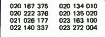
Table 6-6. A Typical Printout from DEBUG.
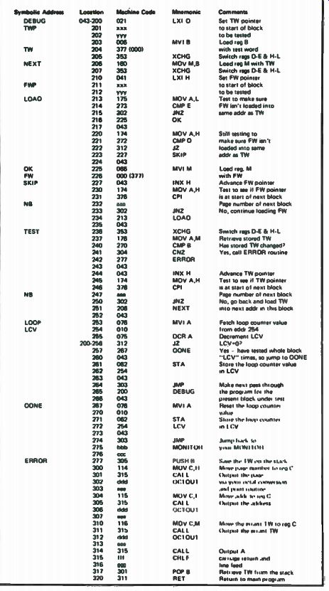
Table 6-7. Improved Memory Diagnostic Program.
Table 6-7 illustrates a typical printout. Note that the page, address and incorrect data are outputted. As in the previous program, this program assumes the existence of an octal conversion and print routine ("OCT OUT") which it can call.
A Few Tips. When you are making the test, do it once or twice with the case off the computer when it is relatively cool. Then put the case on and run through the procedure with the computer thoroughly warmed up. It would be possible to find four defective chips with the program when testing cool and four more when testing hot. Two of the cool defects may show up only sporadically under the hot condition. Also, this is a time when effective use can be made of the spray-type component coolers. You might also wish to sandwich the memory board(s) between other boards in order to entrap the heat.
Build the IC Experimenter To Get Started with TTL and CMOS
For both the novice experimenter and the advanced digital circuit designer, the two most essential tools of the trade are a basic power supply and a suitable signal source. Most modern digital circuit families (DTL, TTL, CMOS and NMOS) either require, or will satisfactorily operate from, a regulated 5v DC source. A one-ampere supply will suffice for most medium-size TTL projects and will more than exceed the needs of even the most ambitious CMOS undertaking. The signal source should provide squarewave (true and complement are helpful) and pulse outputs over a reasonable range of frequencies. A bounce-free variable one-shot output is also an absolute must.
The instrument about to be described will meet all of the above requirements; it is immune to accidental shorts which often occur in the course of trying a new circuit and will, therefore, be a useful addition to any laboratory.
Condensed Specifications. Power supply: 5 ± 0.25v DC at 1 amp, short-circuit proof; automatic thermal shutdown. Astable oscillator: 10Hz to 100 kHz, providing simultaneous true and complementary square waves and 1-us pulses, TTL-compatible, short-circuit protected; manual and/or re mote gating. Monostable oscillator: Simultaneous true and complementary pulses variable from 5-us to 50 ms. TTL-compatible, short-circuit protected; manual or remote triggering. The complete parts list is found in Table 6-8.
Power Supply. The power supply is shown schematically in the lower portion of Fig. 6-32. It is a basic full-wave rectifier, capacitor input supply, followed by an IC regulator capable of delivering in excess of 1 ampere at 5v, while being fully protected against sustained shorts and overloads. The power transformer secondary is rated at 16v c-t at 1.5 amps. These are the minimum parameters to guarantee proper operation under worst case line and load. The IC regulator (7805) has internal thermal protection and must be heat sinked to at least 15 square inches of 1/16" aluminum sheet metal.
Astable oscillator. The heart of the oscillator circuit is U1, a CD 4047 IC. Its operating mode, i.e., astable or monostable, is controlled by the logic state at terminals 4 and 8. As shown in the schematic, with pin 4 grounded and pin 8 high, the astable mode is established. The oscillator may be inhibited by raising the level on pin 4; this is achieved by grounding either of the two inputs of gate U2A. The frequency of oscillation is determined by the charging time of the frequency range capacitors, C2-05. When used in accordance with the IC manufacturer's recommendations, the frequency would be continuously varied by varying the resistance between pins 2 and 3. Unfortunately, this yields a frequency calibration proportional to 1/R and a highly nonlinear dial for a linear taper potentiometer. This problem has been overcome in this circuit by replacing the variable resistor with a variable current source, consisting of Q1 and R2 + R13. The base voltage of Ql, adjusted by linear potentiometer R1, linearly varies the current through R2, and hence inversely varies the effective resistance between pins 2 and 3. A perfectly linear frequency calibration is thus achieved. CR4 and R14 act as a temperature-compensating network for the current source.
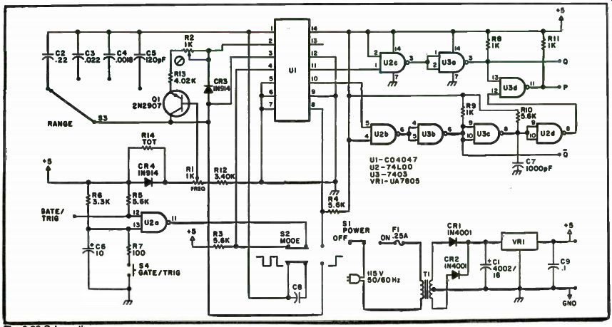
Fig. 6-32 Schematic.
-------------------
Table 6-8. Parts List.
C1 4000 µF, 16 V, electrolytic capacitor C2 0.22 µF C3 0.022 µF matched set, polycarbonate C4 0.0018 uF capacitors C5, C8 120 pF C6 10 µF electrolytic capacitor C7 1000 pF, disc capacitor C9 0.1 µF disc capacitor CR1, CR2 1N4001 rectifier diodes CR3, CR4 1N914 switching diodes F1 0.25 Amp slow-blow fuse 01 2N2907 transistor R1 1000-Ohm wire wound potentiometer R2 1000-Ohm trimmer potentiometer R3, R4, R5, R10 5600-Ohm, 1/4 - Watt resistor R6 3300-Ohm, 1/4 - Watt resistor R7 100-Ohm, 1/4- Watt resistor R8, R9, R11 1000-Ohm, 1/4- Watt resistor R12 3400-Ohm 1%, 1 / 8- Watt, metal film resistor R13 4020-Ohm 1%, 1 / 8- Watt, metal film resistor R14 Trim-on-test, 1/4- Watt resistor, approximately 1000 Ohms Si SPST slide switch S2 DPDT slide switch S3 1-pole, 4-position rotary switch S4 NO momentary push-button switch Ti Power transformer, 115 V 60 Hz primary; 16 V c-t at 1.5 Amps secondary U1 CD 4047AE oscillator U2 74L00 low-power quad two-input NAND gate U3 7403 open-collector quad two-input NAND gate VR1 UA7805 IC voltage regulator Misc. Perforated circuit board, suitable enclosure, line cord, 5-way binding posts, control knobs, fuse clips, hookup wire, solder, hardware.
---------------------
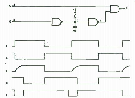
Fig. 6-33. Schematic.
The CD 4047 has an internal divide-by-two flip-flop and therefore produces highly symmetrical square waves at terminals 10 and 11. Gates U2C and U3A couple and buffer the Q output, and gates U2B and U3B act similarly for the Q output of the oscillator. An open-collector gate was chosen as the output device, in spite of its slower rise time, because of its wired-OR capability and its inherent immunity to accidental shorts to ground.
A 1 ps pulse is generated by combining a delayed Q with an undelayed Q. Figure 6-33 shows this circuit and its corresponding timing diagram. As a rule of thumb, a 6000-ohm pull-up resistor and a 1µF capacitor will yield a 1 ms delay. This relation is quite linear with capacitance. If, in your particular application, a pulse width other than 1 ms is needed, just change C7 to the required value.
Monostable Oscillator. The monostable mode is established by grounding U1-8 (through U2A) and by applying a logic " 1" to pin 4. The one-shot is triggered by momentarily raising the level at pin 8. This is accomplished by the output of gate U2A, which will go high when either the GATE/TRIG terminal is grounded or push-button switch S4 is depressed. R7 and C6 act as a debouncing circuit. The period of the one-shot is related to the astable frequency, such that T 1/f. A correction capacitor C8 shunts all range capacitors (C2-05) in the monostable mode.
--
Next: Digital Voltmeters