Brew Up a Signal Generator
For certain aspects of equipment testing and alignment, as well as for circuit experimentation, a good rf signal is a must. Yet many experimenters do not own such a generator because of the cost of one and because it is not as frequently needed an instrument as; perhaps, a scope or a VTVM. This project is a simple rf signal generator that covers from 100 kHz to about 75 MHz in six bands. It is useful for checks of low frequency i-f circuits on up to VHF circuits (using harmonics up to 220 MHz). The cost of the unit can be as low as $5, if one has an exceptionally well-equipped junk box, or it can cost up to about $20-25, in the average case. Still, it is relatively inexpensive for a wide range transistorized and portable signal generator.
The basic generator puts out a CW signal only over its operating range.
Various optional circuits can be added to provide tone modulation and a sweep frequency capability. But we would suggest that these circuits be added later, once the basic generator is functioning properly.
One of the first things to notice about the generator is that there is no frequency readout dial scale. There are several reasons for omitting it.
Usually, the frequency readout scale on most inexpensive generators is more fiction than truth. To do any meaningful alignment work today, one needs a counter to set any signal generator correctly-even some very expensive commercial units. One doesn't need a calibrated scale just to sweep past a 455 kHz i-f or to determine that the front end of an HF or VHF receiver is basically functioning. Lastly, the lack of the not-so-useful scale allows the unit to be far more economically and compactly constructed.
The electrical circuit of the generator is shown in Fig. 9-1. One FET is used as the basic oscillator in a Hartley-type circuit. The second FET is lightly coupled through the 5 pF capacitor in its gate lead to the oscillator.
This stage functions as source follower isolation stage. The last stage, the 2N3866, is designed to boost the signal level up to about 1 volt output on most bands. This level is far more than what is required for most receiver type work, but the increased level comes in handy when doing transmitter exciter work, where the generator might substitute for a vie. The output of the 2N3866 stage can be regulated by the 500 ohm carbon potentiometer, which will provide about a 30 dB variation in output level. A 47 ohm resistor can also be switched in across the output, so a true nominal 50 ohm generator source impedance can be simulated for tests such as receiver
sensitivity. The switching in of this resistor also serves as a high-low output level selector for the generator.
Although the generator is not complicated electrically, its true potential will not be achieved unless it is carefully constructed. Fortunately, no elaborate construction work is required, but attention should be paid to the few details mentioned here. All of the circuitry is mounted on a single-side copperclad board measuring about 2 1/2 " by 2 1/2 ". The board is wired point to-point, using the isolated pad technique, starting with the oscillator stage toward the back panel of the enclosure and progressing forward to the 2N3866 stage towards the front panel. There is nothing critical about the wiring, whatever technique is used, but the circuitry should just be stretched out to provide maximum separation between the oscillator and 2N3866 output stage.
The heart of the signal generator lies in the band-switched oscillator coil assembly and the variable tuning capacitor. The tuning capacitor is a readily available broadcast receiver type, which contains a single section AM section of about 300 pF and a single section FM section of about 25 pF. Such capacitors can often be found with built-in tuning shaft drive reductions of 3:1 to 6:1. The Burstein-Applebee catalog is one source for such a capacitor, although various similar types should be available from Radio Shack, Lafayette and the mail order suppliers. A simple alternative to the AM/FM type is the even more readily available standard dual section AM type, where one section, designed for local oscillator usage, has fewer plates.
Remove more plates from the oscillator section, so it is left with four stator plates and three rotor plates.
The coils for the six bands can either be purchased or constructed from a mixture of home brew and commercial coils. As a completely purchased set, one can use the Conar CO-69 through CO-74 series, at a total cost of $4.
These are replacement coils for an old-fashioned National Radio Institute tube-type signal generator, but they work just fine in this FET oscillator.
The coils are available from Conar, National Radio Institute, Washington, D. C. 20016.
Another alternative is to just purchase the coils for the lower frequency bands, which would be almost impossible to home brew, and wind the other coils. In this case, for the first three frequency ranges one can use pre-wound J. C. Miller-type coils, which have the necessary tapped windings. The types are 9015, 9013 and 9013. For the highest three frequency ranges, one can selfwind the necessary coils on 3/4 " diameter slug-tuned forms. The windings necessary and the tap points for each of the three coils are as follows: 15 turns tapped at four turns from the ground end; seven turns tapped at three turns; and, four and one-half turns tapped at two turns. The latter coil is wound using #18 wire while the other two coils use #24 wire.
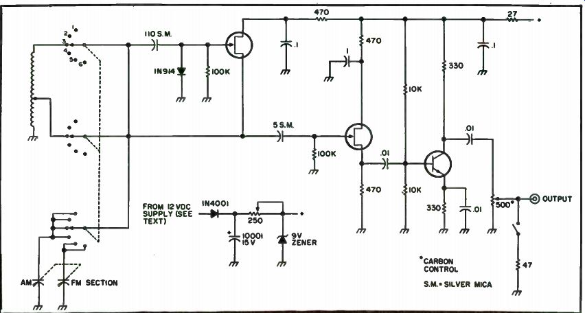
Fig. 9-1. Schematic of the generator. Only one of the six oscillator coils
is shown for clarity. The FETs are HEP802 or MPF102 types. The output transistor
is a 2N706. Other details are covered in the text.
The coils can be mounted directly on the 3P6T rotary bandswitch. The coils are secured to the bandswitch with epoxy cement and wired in place. In order to ensure a good ground connection for the coils, a piece of sheet copper was cut out to resemble a six-legged starfish and placed over the bandswitch shaft, so one of the "legs" could be soldered to each coil. This arrangement is probably a bit overdone. Ground connections from the coils to several ground lugs, equally spaced around the shaft of the bandswitch, should suffice just as well.
The generator is assembled in a standard commercial enclosure, which measures about 5" on each side. The dimensions were based on the size of the band-switched coil assembly, tuning capacitor and circuit board. With a bit of effort, one should be able to fit the generator into the more readily available 4" x 5" x 6" aluminum enclosure.
The generator can be powered either from the AC line or from a 12-volt battery source, making it ideal for both fixed and portable applications. The power supply for the generator is not included in the same enclosure as the generator, and this seems to contribute significantly to the total lack of AC hum on the output signal. The AC power supply is an AC wall plug-mounted 12.-volt DC battery replacement supply of the type commonly sold to power transistor radios.
Within the generator enclosure, and as shown on the schematic in Fig. 9-1, there is only a diode to protect against reverse voltage polarity, a 1000 mF filter capacitor and a 9v zener regulator. For portable application, 12v from a battery pack, or even 9v from a transistor radio-type battery, can be used. The 250 ohm variable resistor before the zener is adjusted for the maximum resistance value that still allows the zener to maintain a constant 9v output.
Because of the lack of a frequency readout scale, there is not the usual need to try to adjust the low and high frequency range excursions on each band. However, they should be checked with a counter to see that sufficient overlap exists between ranges. The slug tuning of the coils suffices to correct the tuning on each range. Although one has some latitude to adjust the frequency coverage on each band to suit individual preferences, Table 9-1 shows a typical arrangement, starting with the lowest frequency band.
The stability of the oscillator proved to be good enough on all ranges except the highest, so that temperature compensation was not needed. This is probably due to the low power operating requirements of the circuit and to the fact that the power supply is mounted externally to the generator. Since the highest band was not used extensively, it was not temperature compensated. But, by selection of small value NPO capacitors placed across the small section of the tuning capacitor and by watching the output frequency change on a counter, it should be possible to achieve excellent frequency stability on the highest range also.
Table 9-1. Typical Frequency Coverage. Band Low end High End
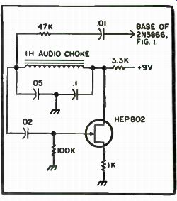
Fig. 9-2. Audio oscillator which can be added to the basic signal generator
to aid in identification of the rf signal.
Tone modulation can be added to the generator by the circuit shown in Fi g 9-2 The circuit provides a single frequency tone modulation, which is useful to identify the presence of the rf signal when working with a receiver having only an envelope (AM) detector. By placing the output of the audio oscillator on the gate of the second FET (instead of on the base of the 2N3866 as Fig. 9-2 indicates), a slight FM modulation of the oscillator will occur. So, the signal generator can be utilized with SSB/CW, AM or FM receivers.
A sweep frequency capability can also be added to the generator, by means of a varactor diode connected across the gate terminal of the oscillator FET to ground, and driven by a suitable sawtooth of triangular waveform. The five for $ 1 varactor diode selections available from Poly Paks are very suitable for this purpose.
You now have the basic construction information needed to put together a very good wide range rf signal generator.
Updated Universal Frequency Generator
Basically, this generator is a collection of IC oscillators and dividers that can generate square waves from the HF range all the way down to the sub-audible AF range and can generate markers all the way into the VHF range. There is nothing sophisticated about the generator, and some of its functions can be performed today by more advanced ICs with even greater versatility. But, the generator is hard to beat as a simple straight-forward device that can be built at a very low cost (none of the ICs costs more than $1.00, except for one optional $3.00 type). It makes an excellent little project for those who still haven't started to experiment with digit ICs.
The uses for the generator are about as versatile as those of a grid-dip oscillator. Also, like such an oscillator which is not a very advanced type of instrument today, one nonetheless always keeps on discovering new and handy uses for the instrument. The board uses still include:
• frequency marker generation
• generation of crystal-stability RF or AF square wave signals
• crystal activity checker
• range extension for present AF or RF generators
• divider chain to allow HF oscillator stability and calibration to be checked by a low frequency receiver for those who lack a counter
The block diagram of this updated generator is shown in Fig. 9-3. It consists of a selectable oscillator section, a fixed string of divide by 10 stages and two divider stages which can be switched in at various points along the divide by 10 stages. The first oscillator is a 1 MHz crystal controlled stage.
Improved circuitry has been used which ensures more stable oscillation with any good 1 MHz frequency standard crystal. An LED indicates that the stage is oscillating. The second oscillator stage can be used with any external crystal extending up to the low VHF range. An LED again indicates that the oscillator is working. The stage can be used as a simple crystal activity checker with the LED, or crystal frequencies can be used which will give some desired output when the oscillator is fed into the divider chain.
The third stage is not really an oscillator stage in itself, but an oscillator input stage. It will accept any external sine or square wave input, condition it and then apply it to the divider chain. The fourth oscillator stage really increases the versatility of the generator. It is a square wave generator whose frequency can be controlled by an external capacitor only. By proper selection of this capacitor, frequencies from several Hz to several MHz can be generated. Thus, in combination with the divider chain, any desired frequency or marker can be generated. The fifth oscillator stage, which is optional, is similar to the fourth oscillator except that it is intended mainly for the entire HF range up to about 25 MHz. Its frequency of oscillation is also controlled by an external capacitor, but its main feature is that it is a voltage controlled oscillator. By varying the voltage with a potentiometer to one section of this stage, a variable or sweep frequency output can be obtained.
The divider chain is a simple series of four divide by 10 stages. The outputs from a 1 MHz input will be at 100 kHz, 10kHz, 1kHz and 100 Hz.
The stages are similar to those found in the timebase of any frequency counter or many crystal calibrators. The two divide by two and divide by five stages can be switched in along the divide by ten string. Using the 1 MHz oscillator input example, the outputs of the divide by two stage will be 500 kHz, 50 kHz, 5 kHz, 500 Hz and 50 Hz. The outputs of the. \ divide by five stage will be 200 kHz, 20 kHz, 2 kHz, 200 Hz and 20 Hz. This example may appear very obvious, but when dealing with inputs other than a simple 1 MHz one, it is important to list all of the various output frequency possibilities to avoid confusion. Of course, looking the other way, that is towards VHF marker frequencies, the listed frequencies represent the intervals at which marker frequencies would appear since the output of the digital stages is a square wave with a very rich harmonic content.
The actual circuit of the generator is shown in Fig. 9-4. Use is made, except for the optional fifth oscillator stage, of only simple SN7400 family ICs. The SN7400 1 MHz oscillator stage makes use of two of the gates for the oscillator itself, one for an output buffer and one to drive the LED oscillator activity indicator. The oscillator can be beat against WWV for accurate calibration using the 25 pF trimmer. Do this by connecting the ...
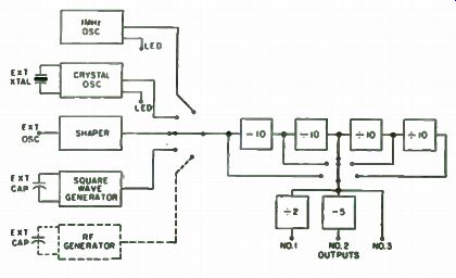
Fig. 9-3. Overall block diagram of the generator.
... output of the oscillator through a small coupling capacitor if necessary, to the antenna input of a receiver tuned to WWV on 5, 10, 15 MHz. During the 10 second tone pause on WWV, adjust the trimmer for zero beat. The second crystal oscillator will operate over a very wide range. The only component that may have to be changed with frequency to ensure stable oscillation is the 150 pF capacitor from one side of the crystal socket to ground. The 150 pF nominal value will operate satisfactorily with most HF crystals. The oscillator range can be extended higher or lower by making this capacitor have a value (in pF) equal approximately to 500 divided by the crystal frequency in MHz. Overtone as well as fundamental mode crystals will work.
The third oscillator, a SN7405, is a hex inverter which uses a single external feedback capacitor to produce a square wave output ranging from a few Hz to several MHz. The capacitor values needed will range from 300 uF to 30pF. The output waveform is not exactly a square wave in the truest sense since the on and off times for each cycle are not exactly equal.
Normally, this will not make any difference, but the situation can be corrected by connecting a 22k resistor from pin 4 to the supply voltage.
The fourth oscillator input stage has been found to function well. About a 1.5 to 2 volt input is required from any external sine or square wave generator to activate the multivibrator. The operation of the stage will be very obvious and even the output from a low voltage filament transformer through a current limiting resistor can be used to check that it is operative.
The fifth oscillator stage, a Motorola 4024, is a very interesting voltage controlled oscillator. Its circuit simplicity belies its very versatile usage. The operating frequency range of this oscillator (multivibrator) is controlled by the value of a single external capacitor connected between pins 3 and 4. The tuning or output frequency of the oscillator within the range established by the fixed external capacitor is determined by a variable 1 to 5 volt DC voltage applied to pin 12. For example, with a 430 pF capacitor between pins 3 and 4, the output frequency range as the voltage on pin 12 is varied between 1 and 5 volts is approximately 200 kHz to 1100 kHz. For a 100 pF capacitor, the range is 5 MHz to 25 MHz. The IC will actually operate up to 30 MHz with a bit of care as to lead dress, etc. The leads to the external frequency range determining capacitor should be kept as short as possible. Also, the ground leads and bypassing to the supply voltage pin should be short or the full frequency range of the oscillator may not be realized. Unlike the SN7400 series ICs which are widely available, one may have to look twice for a source of the MC4024. One source (at $3.00) is Circuit Specialists, P.O. Box 3047, Scottsdale, AZ 85257.
The divide by 10 chain uses SN7490s in their conventional arrangement. Once the layout of a single stage has been determined, the rest need simply be duplicated. They can easily be wired on perforated stock as can the other ICs in the generator.
The divide by two and divide by five stages are all actually contained in one SN7490 which sort of does double duty as a frequency divider.
The construction of the generator depends on individual taste. It can be constructed as an AC powered unit or as a portable unit. As an AC powered unit, a simple power supply using an LM309K regulator is recommended.
My portable unit was constructed in an approximately 3" x 4" x 1 3/4 " metal enclosure. The perforated board was just slightly smaller than 3" x 4" to fit the enclosure. Portable power can be supplied by 4 1/2 volt battery (Burgess 532 or equivalent) or 3 type C or D cells connected in series. There are two main bypassing details, however, which must be observed for good performance and which are not shown in Fig. 9-4 for sake of simplicity. Each IC must have a 0.1 uF disc capacitor going from its supply voltage terminal to ground. Also, a 100 to 500 uF/10v electrolytic must be connected across the battery terminals for a portable unit.
The many uses of the generator have been considerably expanded by these features. It can function as a highly accurate square wave frequency generator (down to fractions of a Hz) at any dividable frequency down from a crystal frequency reference. It can function as a highly accurate marker frequency generator in the HF or VHF range, depending on the crystal frequency reference used. It can produce harmonic markers at any frequency up to VHF by means of its internal oscillator which is variable in frequency. It can serve as a crystal activity checker for almost all fundamental and overtone type crystals. The combination of having a crystal reference frequency oscillator available in combination with a variable AF or RF oscillator allows comparison to be made so one does not fall too far out of range within any variable frequency range.
A final word might be said about the output waveform of the generator.
The output is a square waveform and hence quite rich in harmonic output. It cannot function as a pure, fundamental frequency sine wave generator and was never intended to do so. Reasonably good sine waves can be produced, however, at any output frequency by suitable RC filtering. The situation is very similar to that of filtering a sharply clipped audio signal before it is applied to a modulator stage in a transmitter. Fig. 9-5 provides the details of ...
Fig. 9-4. Wiring diagram. Note that the divide by 5 and divide by 2 functions
use only one SN7490. See text for some details on bypassing by each IC.
Fig. 9-5. Simple RC filter which will help round off square wave output so
a quasi sine wave output can be obtained. Component values should be optimized
using an oscilloscope it possible.
...a two stage RC low pass filter which can be built for any AF to HF frequency to provide a reasonable sine wave output. Of course, LC filters will be better to get a pure sine wave, especially multi-section filters. The formulas for such LC low pass filters can be found in many reference texts on electronics.
Is It the Band or My Receiver?
Probably one of the most frustrating aspects of operation for the experimenter who does not use his station daily for several hours is to know when his station is functioning properly. Whether or not a transmitter is functioning properly can be verified by an in-line wattmeter for power and with a monitor receiver for modulation, at least to see that the rig is basically functioning. Answer check is a good basic check for an antenna system. But, what about the station receiver? An operator who uses his equipment frequently can pretty well judge band conditions on HF and knows that a band is out. But, the infrequent or weekend operator often checks a band and finds signal levels low and then starts to wonder if it is the band or the receiver. Obviously, various checks can be made to see what the real situation is like. If the receiver can tune outside the amateur bands, stations like WWV or selected shortwave broadcast stations can be used as a quick reference to conditions. If a second receiver of equal quality is available, it can be used for verification of the main receiver's condition. But, many experimenter's entire stations consist of a transceiver confined to tuning only the amateur bands.
In this case, some other means of checking receiver performance is necessary. A signal generator providing a calibrated output down to the microvolt would be ideal, but few hobbyists have such test equipment.
This is a different approach in terms of the microvolter. Basically it is a simple gadget-just an oscillator and a carefully made attenuator network to generate a signal of approximately one microvolt. It is compact, battery powered and uses a single transistor. But, it can almost instantly remove all doubt and confusion as to whether a receiver is out or the band is out. It was intended to be used by plugging it into the receiver's antenna terminals to make a check. However, it could be placed remotely and connected to its own antenna to see if an entire receiving system were functioning on any given band. Admittedly, there are pitfalls to this latter approach, since when a signal source is close to an antenna system, good signal pickup may occur even though something has happened to the antenna system to change its directional properties.
The oscillator circuits presented here are mainly for the 20 through 2 meter bands since activity is usually great enough on the lower frequency bands that it is readily obvious if a receiver is functioning. However, if desired, the gadget may be designed to work on any amateur band.
As was mentioned, the microvolter consists of an oscillator and an attenuator network. Many circuits are possible which will work. However, the oscillator must be stable in regard to battery voltage, and construction of the attenuator network, while not critical, must be carefully done to avoid leakage signal paths.
Figure 9-6 shows a typical oscillator circuit which can be used and, by proper adjustment of the components, will work from 20 to 6 meters. It is crystal-controlled for simplicity, and the typical component values for 10 meters are shown. Note that the crystal does not have to have any particular frequency, as long as it falls within the band of interest, so advantage can be taken of the various surplus or odd-frequency crystals available at low prices from such outlets as Jan Crystals. The output is about Y2 volt across 500 ohms, although this will depend on crystal activity and circuit tuning. The resistor attenuator network shown will bring the output down to about 1 microvolt across 50 ohms. The output of the oscillator has to be verified in some manner. The best is, of course, to measure it directly if good instrumentation is available. An alternative is to construct the generator and see what response the entire unit provides on a receiver that is known to be in good shape. After all, the main purpose of the instrument is to provide a quick, relative indication that a receiver has not lost sensitivity. If it can be accurately calibrated as to output it could be used to make direct sensitivity measurements on a receiver in conjunction with a VOM to check audio level changes, in dB, with and without the test signal being applied. A simple LED circuit is included both to indicate that the generator is on and to approximately indicate a low battery voltage condition. The pot in series with the ...
Fig. 9-6. Oscillator and attenuator network. Oscillator may be used on any
band down to 6 meters by proper choice of LC circuit components. Coil: CTC
LS5 form, 15 turns #22 enam., with 2 turn link.
Fig. 9-7. Extremely simple VFO will work down to 2 meters by choice of proper
tank circuit to resonate in desired band.
... LED is adjusted so the lens of the LED is just barely fully illuminated. The difference between this point and no noticeable illumination of the LED is . 15 to . 2 volts for a typical LED. So, it can serve as a battery voltage indicator better than even a cheap meter.
Other crystal oscillator circuits can be used. K1CLL is a very good oscillator which, among other things, features a simple variable output level scheme by means of varying the emitter bias. For those who do not prefer to make their own oscillator, the International Crystal OX oscillator kits are very suitable. They cost only $3 with a tuned output circuit. The Lo kit takes crystals from 3 to 20 MHz and the Hi kit covers 20 to 60 MHz.
Simple VFOs can be used as the oscillator element but here, of course, the problem is that their output will vary with frequency. Nonetheless, if their output variations can be measured, there is no reason not to use them.
For the purpose at hand, ultra frequency stability is not needed, so very simple circuits can be used. Figure 9-7, for instance, is about as simple a VFO circuit as can be desired. The frequency of oscillation is determined by the single LC combination. By choosing combinations which resonate in the various amateur bands, the circuit will work down to at least 2 meters.
Leads should be kept and the oscillator enclosed in a metal enclosure to avoid hand capacity effects.
The attenuator network was shown in Fig. 9-6. Its construction is not critical, but it must be separately shielded even if the oscillator is enclosed in a metal enclosure. The easiest way to do this is by constructing it within a divided enclosure as shown in Fig. 9-8. The enclosure can be of brass sheet, available at many hobby shops, or of copper sheet, or even of sheeting salvaged from old tin cans. The only objective is to completely "button up" the attenuator network so signal leakage does not occur around it to the output jack of the oscillator.
Fig. 9-8. Attenuator must be separately shielded. The output connector should
be mounted on the attenuator shield.
This unit has been kept as simple as possible. There are various ways to embellish it, if desired. For instance, three output attenuator networks with different attenuation characteristics might be built: one as a microvolt output, one as an S9 output (usually taken as 30 microvolts) and one as a 40 dB over S9 output.
Tubeless Partability for the Heath Signal Generator
The Heath IG-102 radio frequency signal generator is a versatile general-purpose wide-range instrument of conventional vacuum-tube de sign which has been catalogued for several years. For those who are still looking for a good signal generator at a moderate price, this article provides a simple, economic and fast means of conversion for portability without sacrificing the original qualities. Modification of the IG-102 gives the instrument new capabilities. These include:
• Battery operation utilizing either dry cells or a nickel cadmium rechargeable bank capable of supplying 7 to 9 volts at a maximum current of 10 to 16 mA.
• With the use of rechargeable nickel cadmium cells of approximately 1.2 volts per cell, six to eight cells are sufficient to provide the required operating supply voltage. The basic radio frequency circuit will operate with a minimum of 4 volts throughout its frequency range. For charging purposes, a self-contained battery-charging circuit is used which employs the original components. These can be dispensed with if dry cells are installed. (Installation of the battery supply is simple, since there is ample chassis space available to mount battery brackets for accommodating the battery units.)
• All tube sections are replaced by four field effect transistors, such as those available from Radio Shack- #,276-1623 or Calectro-#K 4-634 (Fig. 9-9). Some of these Radio Shack #276-1623 packages contain assortments of both rf and af field effect transistors. In testing them, the af types will not oscillate. One particular type which responds well at radio frequencies is the 2N5951. The white-black types are af and do not oscillate at radio frequencies; also, the metallic types are unsuitable.
Procedure for Modification. The following step-by-step instructions apply to changes and additions to the basic IG-102 radio frequency signal generator. Accordingly, the original instruction manual and drawings are used for reference to detail the modification procedure. This procedure involves simple changes, installation of new components and constructions.
Before undertaking the modifications, spend some time studying and re viewing the basic circuit and assembly to become familiar with the original layout. Additionally, study the details of the field effect transistor connection lead designations. In the assortment provided in Radio Shack's #276-1623, three types are referred to in the designation of leads. With reasonable care, there should be no difficulty using any of the transistor types.
Construction.
• Refer to Fig. 9-10, a copy of the original circuit.
• Remove all tubes, if the set has already been constructed.
• Unsolder and disconnect power transformer connections (filament supply line and high-voltage rectifier-filter system), and reconnect the power supply components as shown in Fig. 9-11, using additional components as needed.
• Solder a 75-ohm, 1/2- watt carbon resistor across the R2 (33k, 2W) decoupling resistor used in the original circuit.
• Solder a 90-ohm, 1/2- watt carbon resistor across the R6 (4.9k, 2 W) decoupling resistor used in the original circuit.
• Spot solder one radio frequency field effect transistor across tube socket V1B, terminals 1-2-3, using the lead references given in the transistor package instruction sheet. However, if transistors are selected from the eight-transistor assortment given in Radio Shack's packet #276-1623, then lead orientation should be followed as per the drawing supplied in the packet.
To mount the transistor on the tube socket, do the following: Hold each lead with long-nose pliers (for a heat sink) as solder is applied. Use a 35- to 40-Watt pencil iron with a small blade tip V8" wide and solder alloy 60-40. Apply a small drop of solder to the end of each lead. After thinning the leads, spread them to match the spacing of the lugs on the tube socket. Apply each lead to the required tube socket terminal, as designated. To facilitate connections, also apply fresh solder to the tube-socket terminals.
In spreading the transistor leads, a slight bend on the wire ends will help in making surface-to-surface contact for soldering. With the pliers, hold each lead against the surface of the required tubesocket terminal, and apply the iron to the opposite side of the terminal until solder flows well to form a good spot-solder joint. No mechanical connection is necessary to complicate the procedure. Once the first transistor lead is soldered, it will make the transistor self-supporting, and the remaining solder operation will be easily handled and completed. Remember to use the long-nose pliers as a heat sink for pushing the transistor leads against the tube socket terminals when soldering. Care in soldering and applying the transistor and applying the transistor leads will insure success and avoid thermal or mechanical damage to the components.
• Following the same technique for soldering as explained in the previous step, apply and connect another rf field effect transistor across the tube socket 1A, terminals 6, 7 and 8.
• Apply and connect the third rf field transistor to tube socket 2B, terminals 6, 8 and 9.
• Apply the fourth field effect transistor to tube socket 2A, terminals 1,2 and 3. If another type of FET transistor is used, make certain that the proper transistor leads are used to make connections.
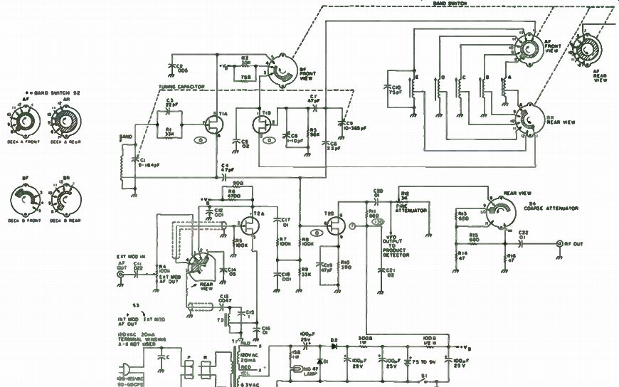
Fig. 9-9. Modified IG-102 circuit. T1 A, T1B, T2A, and T2B-four rf FETs equivalent
to Radio Shack package #276-1623 or Calectro #K 4-634.
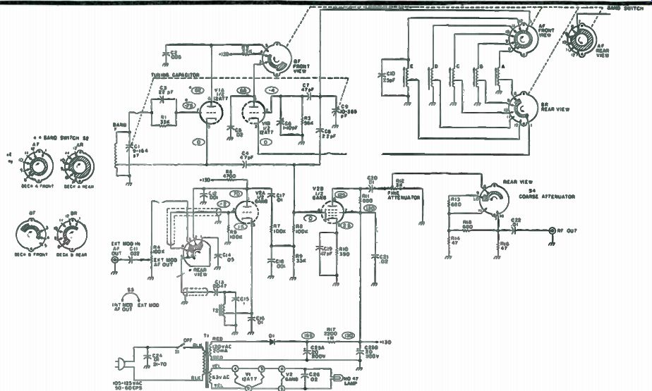
Fig. 9-10. Original IG-102 circuit.
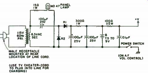
Fig. 9-11. Schematic. MALE RECEPTACLE MOUNTED AT REAR LOCATION OF LINE CORD (USE
TV CHEATER- CORD TO PLUG INTO LINE FOR CHARGING)
Again it may be more convenient for making connections to turn the transistor over (round side up) and cross the D and G leads (use insulated sleeving). This step completes the modification conversion of the basic IG-102 rf signal generator. Additionally, you can install rear tip jacks with the circuit connection leads to permit external testing of the battery supply (+) and (-). Test, Operation and Adjustment.
• Before applying battery power to the circuit, check the positive to-ground resistance to make certain that there is no short circuit or abnormally low resistance reading due to a defective component or wiring condition. Rotate the bandswitch while checking the resistance to ground (which should be several hundred ohms, at least).
• Insert a milliammeter in series with the battery and check the direct current on all bands, which should be 7 to 15 mA. Switching in the audio tone oscillator-modulator will increase it about 1 mA.
• Rf output. A diode detector rf voltmeter applied to the high end of the fine attenuator control (turned counterclockwise for minimum rf output) should indicate about 1 to 1.25 volts on band "A" (low frequency end), and, on each successive band, it will drop off progressively. Nevertheless, rf output should be detectable on all bands.
Vary the tuning on each band from low to high end-the rf voltage should vary smoothly (usually decreasing) without the sudden jumps or fall- off usually associated with parasitic absorption conditions.
• Audio tone oscillator modulator. The AC output of the audio tone oscillator, as measured across the audio output control, should be 1 to 2 volts. Check the tone frequency with a pair of headphones connected to a 0.1 uF coupling capacitor. Finally, use an all-band receiver or grid-dip meter, if available, to check the rf output frequency. The frequency response in each band should be within a few percent and not need any alignment or tuning adjustments.
Heterodyning with broadcast stations will show excellent frequency stability. On band "F," use an identifiable FM station to spot check the frequency calibration in the 88 to 108 MHz range. It may be necessary to squeeze the rf coil to about one-half its original length to get good frequency alignment. Use the long-nose pliers to squeeze turns. To check against an FM station, turn the audio modulation on, connect the rf cable and bring it near the FM receiver's vertical antenna. A good clean modulation note should be heard when the signal generator passes through an FM station.
Conclusion. This original circuit was modified by converting to the battery-operated solid state design, as described. In addition, a three crystal oscillator frequency-spotting standard was installed with a product detector and audio amplifier speaker section. This combination provides frequency check intervals of 100 kHz, 1.0 MHz and 10 MHz, for spot checking the internal six- band vfo or for external testing. Using the crystal standard, heterodyne testing showed excellent frequency tracking and calibration through the six bands. Since there is ample chassis space available, the three-crystal frequency spot circuit is left optional and is merely suggested to you. For this purpose, three crystals and oscillator design data can be obtained from Jan Crystals, 2400 Crystal Drive, Ft. Myers, FL 33901. Additionally, a dual-gate MOSFET product detector, a 250 mW integrated audio power amplifier, a miniature volume control and a 2 1/2 " loudspeaker can be combined to provide the desired frequency-spotting function.
Fig. 9-12. TR4-TR1O-Radio Shack #276-2039 or equivalent; TR11-dual-gate MOSFET;
CT1-Arco 309 padder; CT2-Arco 306 padder; CT4-Arco 465 trimmer; L1 and L2-rfc;
L3-20 turns #30 enamel wire on 2W, 100k resistor.
Figure 9-12 shows a circuit which incorporates the additional features just described-a three-crystal oscillator frequency section with a product detector and an audio power amplifier for monitoring the heterodyne reactions between crystal frequencies and the vfo spectrum. The entire unit can be easily and conveniently mounted in the rf signal generator chassis assembly or separately assembled externally as a sub-unit. Heterodyne activity can be detected up to the 50th harmonic. With additional wave-shaping amplifiers, the harmonic order could be extended considerably, but, unfortunately, that would involve high input current levels which would place excessive demand on the battery power supply.
Fig. 9-13. LF sine wave generator, using Wien bridge oscillator.
VLF Generator
A major deficiency of the older or less expensive sine wave generator is that its output frequency doesn't go low enough for many vital purposes, the dial typically bottoming out at 20 Hz. A principal reason is the unwieldy values of resistance and capacitance required by the oscillator to tune sub-audio frequencies. The instrument about to be described here was designed specifically to complement the workshop sine wave generator by filling in at the low end of the spectrum. It circumvents the tuning problem by providing a number of discrete switch-selected output frequencies.
The frequencies chosen are 1 Hz and 2 to 20 Hz in 2 Hz steps (Fig. 9-13). Given different circuit values, however, the instrument is capable of a much wider range, as will be indicated. Maximum output amplitude is 3 volts rms or 8.5 volts peak-to-peak. A pot-and-switch attenuator allows the . output level to be set with a fair degree of precision to any value within a range of five decades. The unit is powered by two 9 volt batteries of any type. Performance does not suffer until either battery potential drops below 6 volts.
How it Works. As shown in the circuit diagram of Fig. 9-13, the sine wave generator employs a common IC, the popular type 741, in a Wien bridge oscillator. This kind of circuit is characterized by a four-element r-c network connected in the feedback path of an amplifier. The four elements are R6 in parallel with the capacitor selected by S2A, and R7 in series with the capacitor selected by S2B. This network is connected in the positive feedback path of IC1, so oscillation occurs at the frequency where zero phase shift occurs. The two selected capacitors are always equal in value, to keep the reactance of the parallel combination the same as the series, so that the voltage-dividing action of the network gives the same amount of feed back at any frequency. The selection of these capacitors is discussed under the heading "Choice of Parts." The gain of the amplifier, and hence the amount of positive feedback necessary to sustain oscillation, is determined mainly by the setting of output adjustment R3 in the negative feedback path. However, feedback in a sine wave oscillator is very critical; too little and the oscillator quits, too much and it saturates, generating a square instead of a sine wave. Nonlinear elements are usually introduced to deal with this problem. One system uses a lamp or thermistor where we have connected R3. Current sensitive elements such as these, however, introduce perturbations due to thermal inertia. Another method uses a voltage sensitive element like a zener diode, connected in the positive feedback path.
Zener diodes, though not suffering thermal undulations, have a deleterious effect on oscillator waveform, tending to flatten the peaks. We have introduced a variation of the zener idea. Ordinary silicon diodes CR1 and CR2 constitute the required nonlinear load, but waveform distortion is minimized by the mitigating effect of series resistor R8. This scheme yields a good sine wave without making the adjustment of R3 terribly critical.
A small DC offset results from the constraint offered by higher resistance in the positive input of the op amp than in its negative input. Hence offset adjustment R2 is provided to set the average output level of the op amp to zero, as described later under the heading "Adjustment." Due to the shunting action of the network R8, CR1 and CR2, the formula normally used to find the frequency of a Wien bridge oscillator does not apply to our instrument. Furthermore, since this is a nonlinear network, frequency depends somewhat on the amplitude of the sine wave appearing across it. As a practical matter, with R3 adjusted to give a signal of 8.5 volts peak-to-peak at pin 6 of IC1, the oscillator frequency is f = 0.6/C, where C is the value selected by S2A or S2B, in uF. It is important to keep in mind that the setting of R3 does not have an effect on frequency. Also, be advised that R2 and R3 interact slightly.
Choice of Parts. Frequency is determined by the two capacitances selected and by R6, R7 and R8. Precision resistors are recommended for...
Table 9-2. Capacitance Values.
...use in these latter three circuit locations to give you the best chance of achieving the same output frequencies. Also, a precision resistor gives better long-term stability than an ordinary carbon composition type.
Likewise, stability is best served by using high quality film capacitors.
Ceramics would be a dubious choice due to reports of frequent problems with stability, leakage, temperature sensitivity, tolerance, power factor and just plain open circuits (especially when capacitors of this type are obtained on the surplus market). Electrolytics or other types that polarize should not be considered.
If you want the output amplitude of the generator to be exactly the same for every setting of FREQ switch S2, the two capacitance values selected in each position must be matched exactly. Note that most of the values in Table 9-2 were obtained by connecting two capacitors in parallel.
For example, C1 and C12 are each 0.6 uF, achieved by paralleling 0.5 uF and 0.1 uF. The two 0.5s should be matched and so should the two 0.1s. Use a capacitance bridge for this selection job. Of course, the closer the actual value of the capacitors to the figures given in the table, the more accurate will be the frequency settings.
If you don't have a capacitance bridge, you can match the capacitors in-circuit. Two capacitors are matched if the output level remains the same when they are interchanged. However, this cut-and-try method is tedious and tricky at best. Therefore, to keep the adjustment procedure reasonably short, we will proceed on the assumption that you have somehow managed to match the capacitors or else don't care if the output level varies slightly . from one frequency setting to the next.
You may wish to extend the frequency range of your instrument. There is no lower limit, but the upper is dictated by the op amp itself, output amplitude suffering beyond about 5 kHz. Using a high frequency range to about 20 kHz. Also, it helps to connect a small capacitor from pin 2 of the op amp to common. The value is best determined experimentally but 250 pF would be typical.
Position 12 of S2 was left unused to permit the addition of jacks for external capacitors, if test signals outside the present frequency range of the device are required.
Construction. There are no special precautions to be observed in construction. The instrument can be built in a 5- 1/4 " x 3" x 2-e LMB box chassis No. 136. This box is admittedly a bit smaller to comfortably accommodate all those capacitors so you would be smart to use a bigger one.
The IC and a few other small parts can be wired onto a perfboard, which is then mounted to the chassis box by a spacer.
The batteries can be mounted inside the cover with double stick tape.
Adjustment. If you are using precision resistors for R6, R7 and R8, and have carefully selected the capacitors, the probability is very great that your output frequencies will be right on the money, and all you need for testing and adjustment is a VOM. If you wish to check output frequency, you will of course need suitable test equipment such as an oscilloscope with accurate timebase. To adjust the sine wave generator, proceed as follows:
• Set offset adjustment R2 to its minimum voltage, or ground, position, MULT switch S3 to the 1 position, VAR control R13 to its maximum output position and FREQ switch S2 to 20 Hz.
• Connect a VOM to output terminals J1. Set the VOM to measure AC voltage and adjust R3 to obtain 3 volts rms. (Don't use the "output" feature if your VOM has one, because its coupling capacitor may not be big enough to pass 20 Hz without some attenuation).
• Set the VOM to measure DC voltage on its lowest range and adjust R2 to obtain zero volts.
• Repeat the second and third steps until no further adjustment is necessary.
You may now calibrate the VAR control if desired. Your instrument can be calibrated in terms of peak-to-peak voltage, but you may prefer to use rms instead. An oscilloscope is more convenient to obtain values in the former units, a VOM in the latter.
If you have access to an oscilloscope, check frequency and amplitude of the sine wave at various switch positions. Variations in amplitude are caused by imperfect matching of the capacitor values. Errors in frequency at some switch positions but not others means inaccurately selected values.
If all frequencies should prove to be off by about the same percentage and in the same direction, the problem is easily solved by changing the value of R8 as required to make the output frequencies exactly correspond to the dial markings. Raising or lowering R8 by 20 percent lowers or raises the frequency by about 8 percent. However, varying R8 changes feedback, so you should repeat the adjustment procedure each time you try a different value.
There are no special tricks to operating the instrument, but remember that the output is DC coupled and a suitably large capacitor or some other means of DC translation is needed if you wish to drive any conductor on which DC is present.
A small DC offset appearing in the output as the minus battery runs down can be balanced out, if necessary, by touching up offset adjustment R2. For a complete parts list for this project, see Table 9-3.
--------------

Table 9-3. Parts List.
B1, B2 -9 volt battery CI-C22 -Film capacitors ( values given in table, see text for discussion of matching CR1,CR2 -1N914 diode (Ci -Op amp, Fairchild Type FU5B7741393 or equivalent JI -Dual binding post, red and black H H Smith Type 269RB RI -47,000 Ohm, I/4 Watt resistor, t' R2 -1000 Ohm miniature potentiometer, Mallory MTC-13-L. R3 -5000 Ohm miniature potentiometer, Mallory MTC-53-L1 R4 -8200 Ohm, 1/4 Watt resistor. 54 R5. R10 -100,000 Ohm, 1/4 Watt precision resistor, 5'4 R6. R7 -1 megohm, 1/4 Watt precision resistor. 1r4
R8 -100,000 Ohm. 1/4 Watt precision resistor, 1 , 4
R9 -9100 Ohm, 1/4 Watt resistor, 5'4.
R11 -1 megohm, 1/4 Watt resistor. 5 , 4
R12 -10 megohm, 1/4 Watt resistor, 5 , i R13 -1000 Ohm linear potentiometer Si -Toggle switch, double pole single throw S2 -Rotary switch. 2 pole, 12 position Misc. parts-Battery connectors (2), perfboard, knobs with indices (3), suitable chassis, mounting hardware, etc.
-------------------
Build an FM Signal Generator
The OSCAR amateur satellites have caused a renewed interest in VHF and 10 meter preamplifiers. Most of these preamps provide enough gain and noise improvement to allow them to be used with older general coverage receivers and surplus commercial "boat anchors." In order to be effective, however, the receiver used behind any preamp or converter must be properly aligned. Many available receivers employ a 455 kHz i-f section, which must be properly adjusted for optimum receiver performance. however, many hobbyists do not possess the signal generator necessary to adjust i-f stages, and unfortunately, many older kit type generators do not remain stable long enough to complete the tune-up.
This project is an easy to build FM fixed frequency signal generator for 455 kHz. It uses two readily available ICs, a 8038 function generator and a 741 op amp. A deviation control and output level control are provided, but the frequency is calibrated at just one frequency. It is possible to change the value to work with any i-f under 500 kHz by simply changing resistance or capacitor values. Because of the use of ICs, the other parts required are relatively small. Even the power supply is optional if a good regulated 6 volt positive/negative supply is available.
The construction of a 2 meter receiver promoted the designing of this generator. The need for an FM signal generator had existed for several years, but this receiver construction forced the issue. A search of electronic catalogs showed that there really are no lower priced FM generators available, even in kit form. Next the government surplus list was reviewed with similar results. There are surplus units, but prices are very high, cover much wider spectrum than required and have many modes of modulation. At that point, the design specs were set up with cost and availability of parts as prime considerations.
Circuit Description. Some information has been written on the 8038 function generator, but really not enough. It is a very useful device putting out sine, square and triangular waveforms of a quarter volt or more in amplitude (Fig. 9-14). Frequency range is from a small fraction of a Hz to about 1 MHz. Only a few external resistors and a capacitor are required to finalize the generator. Since an audio generator was already available for this project, it was decided to not make use of the full frequency capability of the 8038. Triangular output is available on pin 3 and the square wave by making the 10k resistor on pin 9 a pot.
The frequency of the generator is determined by the RC combination of C1, the 120 pF capacitor (mylar or polystyrene recommended), the series resistance of R3 (500 ohms) and the 680 ohm resistor. The variation of R3 shifts the generator frequency over a range of about 100,000 Hz. The 500 ohm pot across pins 4 and 5 sets the duty cycle or symmetry of the wave shape.
The generator output is taken from a voltage divider connected to pin 2, the sine wave output. An output of over 100,000 e is available at this point.
The output level can be modified by changing the ratio of the 10k and 4.7k ohm resistors.
FM modulation of the 8038 is obtained by applying a small varying signal between pins 7 and 8 and the positive voltage supply. This modulation voltage is obtained from a simple audio oscillator using just one IC, a mini-dip 741. Other op amps can be used, but experience has shown the 741 is one of the easiest to work with and the cost is very low.
This oscillator uses a notch network from the opamp output to the negative input. The result is a sine wave oscillation at about 1000 Hz. This signal is applied to the generator through the interstage transformer after being reduced in level by the resistor network.
The power supply is a simple bipolar (positive and negative) supply which is zener regulated and well filtered. The transformer can be two separate 12.6 volt units or a single 25.2 volt unit with a center tap. The four diodes could also be a rectifier bridge with at least 100 volt piv rating. This power supply could be eliminated if a good 6 volt bipolar supply is available.
However, in this case, since it appeared much use would be made of the generator and since the power supply is quite inexpensive, it was built into the final unit.
Fig. 9-14. One 25.2 V 300 mA CT or two 12.6 V 300 MA (primary in parallel,
secondary in series). All fixed resistors 1/ 4 Watt. Capacitors greater than
1 in pF, less than 1 in uF, unless otherwise marked.
Construction Details. In the original unit, the audio oscillator, frequency generator and power supply were each mounted on individual perforated boards. This was necessitated by several design changes made along the way. Packaging seems to work out best with the oscillator and generator on the same board, with the power supply separate.
Generally, construction is not critical, but the usual good construction practices should be followed. The entire device, including power supply, can be mounted in a 3" x 4" x 5" minibox. The output level control, R2, the deviation level control, RI, and the output connector (BNC type) are mounted on the front panel. Since the output frequency is set at 455 kHz, this pot is mounted inside. The power cord is brought in the back, the transformers are mounted on brackets to the top and sides of the case.
Calibration. After checking all wiring several times, check it once more.
Apply power to the generator and check to make sure that both plus and minus voltages are about 6 volts with correct polarity. With RI set to the low end, look at pin 2 of the 8038 or the output of R2 with a scope. The correct setting for the 500 ohm pot between pins 4 and 5 on the 8038 is about the midpoint. If the output is badly distorted or is missing, adjust that pot to obtain a clean looking sine wave.
The next step is to adjust the frequency with R3. The best method of adjustment is with a frequency counter or meter. While continuing to monitor the waveform on the scope, adjust R3 to the proper frequency, 455 kHz. There will be interaction between the 500 ohm pot and R3. Continue to adjust back and forth until a good sine wave at 455 is obtained.
If a frequency counter or meter is not available, a receiver with known 455 kHz i-f could be used. By applying the generator output to an early stage (at low level) and measuring the output of the last amplifier stage, a peak in output would indicate the generator is set to the same frequency as the receiver i-f being used.
The only remaining item to check is the audio oscillator. Attach a scope or AC voltmeter across R1. There should be a good sine wave of several hundred millivolts present at about 1000 Hz. The generator is now fully operational and the box can be closed up. To actually look at an FM signal, connect a scope to the output of the generator. With R2 at full output, slowly advance the deviation control, R1. The trace should spread or smear horizontally as the control is advanced. Notice that there is no increase in amplitude since this is strictly frequency modulation. The FM generator is now ready for use.
Conclusions. The unit can be used to align the i-f amp and quadrature detector of an FM receiver under test. The unit is stable and provides more than ample deviation required for hobbyists work.
FM Alignment Oscillator
Surplus commercial transceivers still provide the most economical means of getting started on the amateur FM bands. Often, however, these rigs require considerable tweaking to bring them into our bands. An rf signal source to align the i-f and rf sections of the receiver is almost always required to accomplish tune-up.
This is a simple test oscillator built around the ever popular International Crystal "OX" oscillator board. Two oscillators provide a 10.7 or 21 MHz signal for i-f tune-up and a low level signal for rf section alignment. The crystal selected for rf alignment is in the range of 6 to 10 MHz-a harmonic provides output on the operating frequency. The 24th harmonic for two meter work was chosen here and has successfully tuned several 430 MHz rigs utilizing the 50th harmonic of a 9 MHz EX crystal. This allows an "OX-LOW" oscillator to be used in both sections of the test unit.
Construction. The unit consists of a 5" x 2 1/2 " x 2 1/2" minibox with a SO-239 coax jack and a SPDT switch mounted in opposite ends (Fig. 9-15). The two OX oscillators mount side-by-side with the supplied hardware. The rf output of one oscillator is directly connected to the output jack, with the second link coupled to the coil of the first with two turns of # 18 insulated wire. This prevents the output of one oscillator being shorted by the other.
The switch selects the oscillator to be powered by an external 9v battery.
Fig. 9-15. Block diagram. Link consists of 2 turns # 18 around L2; cold end
of L3 is not grounded. SW1 is a center off SPDT.
Operation. The i-f crystal should be placed in the link coupled oscillator, as the strong fundamental output is utilized. When using the high frequency harmonic, directly couple the test unit output to the antenna of the rig. When the rf section is rough tuned, the oscillator is moved across the bench with a 10" section of wire serving as an antenna. The noisy, not fully limiting, signal is then used for tuning of the receiver.
Although the EX crystal is of low accuracy (by FM standards), there is seldom a case where tweaking the receiver first oscillator trimmer did not tune the harmonic, even in the case of the 50th harmonic used for 430 MHz units.
The EX crystal frequency for the FM bands may be determined as follows:
144 MHz-Fx=Fo/24 220 MHz-Fx=Fo/20 430 MHz-Fx=Fo/50
...where Fx=frequency of EX Low crystal, and Fo=receiver frequency.
This unit is an invaluable aid in tuning a variety of surplus rigs. Once the rough tuning is complete, the rig may be netted by monitoring another ham or the output of your local repeater and zeroing the discriminator.
SSTV Test Generator
Probably the biggest obstacle facing hobbyists building their own SSTV monitor is finding a stable slow scan signal source to properly adjust the monitor circuitry. This is especially true if the reader decides to design his own monitor or deviates from an existing design. The monitor itself generally cannot be used as a test unit because all the circuitry has to be adjusted and operating properly before anything can be viewed on the monitor's CRT. This is an SSTV pattern generator which produces a continuous, high quality, 4 x 4 checkerboard SSTV signal which can be used with a triggered sweep oscilloscope to follow the slow scan signal through the monitor circuitry. The generator can be used to improve the design of an existing SSTV monitor or as a diagnostic tool to repair one. This pattern generator is an adaptation of a circuit designed by Bert Kelley K4EEU. NE555V timers are used as astable oscillators in place of the crystal oscillators, and in digital logic has been modified to produce a 4 x 4 checkerboard pattern.
You'll appreciate the need for such an instrument when you seriously begin designing and building your own monitors. Anyone undertaking such an adventure should have a similar instrument.
The front end of one hobbyists monitor contained a conglomerate of designs and circuitry. Breadboarding the circuitry was relatively easy for him, but finding a stable signal source proved to be the biggest problem. He was able to use an audio oscillator to initially adjust the limiter, pulse counting discriminator, video amplifier and sync separator, but fine tuning them for maximum performance was impossible using this method. A cassette recorder was used for a time, but was unsatisfactory from his standpoint because the video content was constantly changing, as was the video quality.
Fig. 9-16. 555 timer connected as an astable oscillator. C1 is recommended
by the manufacturer.
1200, 1500 and 2400 Hz Reference Oscillators. The primary attraction of the K4EEU generator is its inherent stability, accuracy and lack of adjustments provided by three crystal controlled reference oscillators. This hobbyist felt, however, that the stability of 555 timers was adequate for most SSTV alignment applications and he designed his generator accordingly.
Several dozen Signetics NE555V timers manufactured over a two year period were tested over a temperature range of 25° C-55°C in an oil bath to determine their temperature coefficients (tempcos) and, therefore, their stability as reference oscillators when operated in the astable mode. A test fixture was constructed so that only the NE555V was placed in the oil bath and not the external timing components. Figure 9-16 shows a 555 timer connected as an astable oscillator. The tempcos of the NE555V timers measured . 045 percent to . 07 percent per degree centigrade (/°C). After the tempcos of the 555s were determined, a number of different timing components were included in the oil bath to check the overall oscillator tempcos. Best performance was obtained using precision wirewound resistors and metallized polycarbonate film capacitors with oscillator tempcos measuring . 05 percent to . 08 percent C. The worst performance was obtained using carbon resistors and disc ceramic capacitors with oscillator tempcos exceeding . 3 percent /°C. As a compromise between performance and parts availability, he used RN55/60C (50 ppm) metal film resistors, cermet 15 turn trimpots and metallized polyester capacitors. Using these components, oscillator tempcos did not exceed . 1 percent C, which corresponds to 1.2 Hz/°C for the 1200 Hz sync oscillator, 1.5 Hz/°C for the 1500 Hz black oscillator and 2.4 Hz/°C for the 2400 Hz white oscillator.
Circuit Description. Referring to the schematic in Fig. 9-17, U1, U2 and U3 are 555 timers used as 2400 Hz, 1500 Hz and 1200 Hz reference oscillators. The component values specified in Table 9-4 have been selected so that the oscillator frequencies can be adjusted ± 16-19 percent from nominal to allow for normal component variations. The pattern generator pin assignments can be found in Table 9-5. To improve the oscillator's ability to be set, R2, R5 and R8 can be changed to 2k and R4, R7 and R10 trimmed (selected) for the correct frequency. There is nothing critical about the values specified and they can be changed as required, but keep the duty cycle in the 47-49 percent range. Table 9-6 provides nominal values of Rb for preferred values of C when Ra equals 1k. Nominal values include 1/2 the value of the series trimpot selected. The outputs of U1, U2 and U3 are brought out to pins C, B and A.
Fig. 9-17. Schematic, SSTB pattern generator.
------------
Table 9-4. Parts List.
C1, 2 .22 uF ± 10% 250 V C3, 4, 6, 8, 11, 14 .01 uF ±10% 250 V C5 .015 uF ±10% 250V C7 .022 uF ±10% 250 V C9, 12 .001 uF disc ceramic C10, 13 .047 uF ±10% 250 V C15, 16, 17 .1 uF ±10% 250 V Note: With the exception of C9 and C12, all caps are metallized polyester Mepco/Electra Series C280AE/A or equivalent (.4" lead spacing). CR1, 2 1N914 or equivalent silicon R1 1 k ± 10% carbon R2, 5, 8 10k ± 10% 89PR 15 turn cermet trimpots; R3, 6, 9 1k ± 1% RN55/60C 50 ppm metal film R4 24.3k RN55/60C 50 ppm metal film R7 26.7k RN55/60C 50 ppm metal film R10 21.5k RN55/60C 50 ppm metal film R11, 14 12k ± 10% 1/2 Watt carbon R12, 15 10k ± 10% 1/2Watt carbon R13 102k ±1% RN55/60D 100 ppm metal film R16 619k ± 1% RN55/60D 100 ppm metal film U1, 2, 3, 6, 7 NE555V IC Timer U4 7410 triple 3 input positive NAND gate U5, 8 7400 quadruple 2 input positive NAND gate U9 74132 quadruple 2 input positive NAND Schmitt trigger U10 7474 dual-D type positive edge triggered FF Ull 7492 divide by twelve counter U12 7490 decade counter
--------------------
U4 is a TTL 7410 three input positive NAND gate. U4A and U4B alternately gate the 1500 Hz black and 2400 Hz white oscillators to the input of U4C, except when inhibited by the SYNC signal from U5C. During the time that U4A and U4B are inhibited by SYNC, USA is enabled by the SYNC signal from U5D, gating the 1200 Hz sync oscillator to the input of U4C. U4C is as used a three input inverter, its output, the SSTV video output, brought out to pin 3.
U5 is a TTL 7400 quadruple 2 input positive NAND gate used as a sync adder, combining the 5 ms horizontal and 30 ms vertical sync pulses from U6 and U7. The outputs from U5D and U5C (SYNC, SYNC) are brought out on pins L and K. U6 and U7 are 555 timers used as 30 ms vertical and 5 ms horizontal sync generators. U6 is triggered from the negative edge of U10A ( 15Hz) and U7 is triggered from the negative edge of Ul 1 ( V8Hz). Pin 6 may be externally grounded to increase the horizontal sync pulse width from 5 ms to 30 ms. This provides a 30 ms wide sync pulse at a 15 Hz rate for easily
----------------

Table 9-5. Pattern Generator Pin Assignments.
1 Vertical Sync Pulse, 30 ms wide 2 Horizontal Sync Pulse, 5 ms wide 3 SSTV Video 6 Contact closure to ground increases the width of the horizontal sync pulse from 5 ms to 30 ms.
9 Ground A 1200 Hz B 1500 Hz C 2400 Hz F Power in, +5V -±-. 25 - 2 150 mA H 6.3-12.6 Vrms AC e 6-12 mA K Sync (combined horizontal/vertical)
L Sync (combined horizontal/vertical)
------------------
... adjusting the monitor's vertical sync separator. The outputs from U6 and U7 are brought out on pins 2 and 1.
U8 is a TTL 7400 quadruple 2 input positive NAND gate. U8C com bines the output of U9C and U9D and in conjunction with inverter U8D, alternately enables/disables gates U4A and U4B. U8B is not used.
U9 is a 74132 quadruple 2 input positive NAND Schmitt trigger. U9A squares the 60 Hz AC input pin H providing fast output rising/fall times, the positive edge triggering the first dual-D FF U10B. U9B is used as an inverter for the 1 Hz output of U12.
Opposite phases of the 30 Hz output from U10B and 1 Hz output from U12 are connected to U9C and U9D, which alternately gate the 1500 Hz and 2400 Hz oscillators every 30 picture lines and 16.67 ms producing a 4 x 4 checkerboard pattern.
U10 is a TTL 7474 dual-D type positive edge triggered FF triggered by the positive edge of U9A. U10A and U10B divide the 60 Hz output from U9A by four, producing the 15 Hz SSTV horizontal scanning frequency. The negative edge of U10A triggers the 5 ms horizontal sync generator U6 and
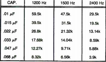
Table 9 - 6. Nominal Values.
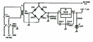
Fig. 9-18. This power supply satisfies the requirements for the pattern generator,
but since the generator only requires 150 mA +5 V, it can easily be borrowed
from an existing supply.
U11. Both phases of U10B (30 Hz, 30 Hz) are connected to the inputs of U9C and U9D. U11 is a TTL 7492 divide by 12 counter and U12 is a TTL 7490 decade counter connected to divide the 15 Hz horizontal scanning frequency by 120, generating a 30 ms vertical sync pulse at the end of 120 lines or 8 seconds.
Each counter contains a +2 element combined with a + 5 element (7490) and a + 6 element (7492). The schematic is not typical of two cascaded counters as follows: 7492- + 6, 7490- + 5, 7490- + 2 and 7492- +2. This connection provides the vertical scanning logic which produces the symmetrical 4 x 4 checkerboard pattern when combined with the horizontal logic in U9C and U9D. In truth, the 4 x 4 checkerboard pattern is not symmetrical as displayed on a monitor, as 5 ms of the leading edge is blanked by the horizontal sync pulse; that is, the 1500 Hz and 2400 Hz oscillators are overridden by the 1200 Hz sync oscillators during the horizontal and vertical sync pulses.
Construction: Printed Circuit Board. The components are mounted on a double-sided 5 1/2 " x 3" glass-epoxy circuit board fabricated to fit a standard 10 pin card edge connector with . 156" spacing. You may prefer not designing double-sided circuitry because of the problems encountered making them at home and the increased costs involved, but the artwork density using twelve ICE made it impossible for this hobbyist to design single-sided circuitry which fits a 5 1/2" x 3" circuit board. The artworks were prepared at home using commercially available artwork aids, taped 2:1 and photographically reduced at a local photo shop. Using direct positive photo-resist coated boards available from the Vector-Electronic Co. (CU70/45WE-2RN, 7" x 4k". 1/1(" double-sided glass-epoxy), the boards were exposed, developed and etched following the instructions that came with the boards.
After cutting and drilling (#65 drill for IC pads, #60 drill for others), he tin plated the finished boards with Shipley LT-25 chemical plating solution.
After assembly, the component side is top soldered as required and jumpers soldered top and bottom in the three feedthrough holes.
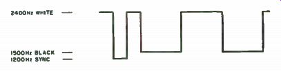
Fig. 9-19. Output of the WB9L VI low pass filter.
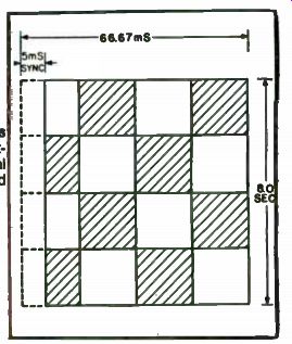
Fig. 9-20. Checkerboard pattern as displayed by the monitor. The pat tern
appears to be unsymmetrical because the leading edge is blanked by the 5 ms
horizontal sync pulse.
Adjustment. Obviously the easiest way to set the 1200 Hz, 1500Hz and 2400 Hz reference oscillators is with a frequency counter, and the values specified in the parts list should allow you to adjust the oscillators without reselecting R4, R7 or R10. If a frequency counter is not available, the oscillators can be set with a triggered scope with a calibrated timebase. Set the timebase to . 1 ms/div, internal trigger and adjust the 1200 Hz oscillator for a width of . 83 ms, the 1500 Hz oscillator for a width of . 67 ms and the 2400 Hz oscillator for a width of . 417 ms. Switch to line trigger and readjust the oscillators for a stable waveform-(i.e., a waveform which is not slowly drifting from right to left or left to right across the screen). This adjusts the oscillators against the 20th harmonic (1200 Hz), 25th harmonic ( 1500 Hz) and 40th harmonic (2400 Hz) of the 60 Hz power line and is accurate within 0.1 percent provided your timebase is calibrated, as it is very easy to adjust the oscillators against the wrong harmonic.
Operation. The pattern generator requires +5v ±-0.25 at 150 mA and 6.3-12.6 Vrms AC, and the supply illustrated in Fig. 9-18 satisfies the power supply requirements for the generator.
Syncing the scope on the positive edge of the horizontal sync pulse will be adequate for most troubleshooting designs to repair an ailing monitor with the generator. The 1200 Hz output can be used to tune the sync circuitry, ...
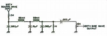
Fig. 9-21. This low pass audio filter used by K4EEU requires no power supplies.
...and the 2400 Hz output can be used to adjust the discriminator. The horizontal and vertical sync pulses may be used as horizontal and vertical discharge pulses to drive the triggered deflection circuitry, and the checker board pattern can be used to optimize the gain(s) of the low pass filter for a square wave response with just enough overshoot (ringing) to enhance picture detail. The video output can be attenuated with a potentiometer to determine the minimum input for limiting, determined by limiter gain. Figure 9-19 is the output of the WB9LVI low pass Butterworth filter with the generator connected, and Fig. 9-20 illustrates the checkerboard pattern as displayed by the monitor.
Although designed primarily for tune-up, calibration and repair, the generator can also be used for transmission by using low pass audio filter as shown in Fig. 9-21 to convert the square wave video to sine waves. This filter requires no power supplies, but an alternative is the filter used in Fig. 9-22.
Conclusion. Compared to the cost of an SSTV monitor, the pattern generator represents a modest investment. Naturally, a monitor can be constructed and aligned without this, but it should save countless hours of work should a snag develop.
Master Sync Generator
This master sync generator is designed to produce interlaced sync for a black and white camera at minimum complexity and cost. The heart of this circuit is an IC made by Texas Instruments for the '74 series of Sylvania color TVs.
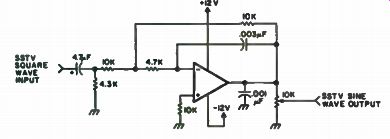
Fig. 9-22. WLMD low pass audio fitter.
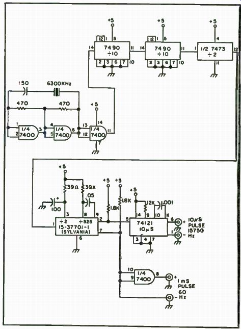
Fig. 9-23. Schematic.
This IC, Sylvania part number 15-377701-1, is a +2, a + 525 and a single-shot all-in-one 14 pin dip IC. The list price is $5.40, and the net price is proportionately lower. This IC was designed so that the TV set generates its own sync signals if off the air snyc is temporarily lost.
By putting in a 31.5 kHz signal, and adding a single-shot to the horizontal output lead, interlaced sync results. One method of getting 31.5 kHz is shown in Fig. 9-23. With a surplus 6300 kHz xtal in the junkbox, this hobbyist followed it with a + 200 set of flip-flops. Many other combinations of xtal and dividers would work fine, such as 3150 kHz and + 100, 504 kHz and +16, etc., or you can pay the long dollar for a 31.5 kHz xtal.
Digital Signal Source
There seems to be a lack of a suitable signal source in this day and age.
One hobbyist tried several things, including squaring circuits on the wide range rf generator and several pulse/function generation units, with only marginal success. Recently, while working on a frequency synthesizer, an idea occurred to this experimenter that after breadboard construction seems to be the answer. Development of this idea will result in a square wave signal source covering from 20 MHz down to sub-audio in fully tunable decade steps. It has proven to be an ideal unit for experimenting with amateur radio applications of TTL and CMOS logic.
Theory. The basic idea as presented in Fig. 9-24 is for a tunable oscillator in the 10 to 20 MHz range with switchable decade dividers for the range selection and switchable binary dividers for band selection. The resulting frequencies and time constants are listed in Fig. 9-25.
Construction. Figure 9-26 is the oscillator that this hobbyist used.
Others would do as well. Try your favorite-just be sure the output is adequate to drive the digital buffer. Drive requirements to the first TTL stage can be cut down by biasing that stage into its linear range with a 2.2k resistor to ground as indicated in Fig. 9-26.
Figure 9-27 represents the power supply circuitry and is self explanatory. Figure 9-28 includes the dividers and output circuit. Construction is straightforward with few precautions. It would be wise to keep all divider-to-switch wires separated from each other slightly (just don't bundle them all together in a cable harness). Run a separate power and ground lead for each IC. That way you need only one bypass capacitor on the common +5 volt and ground point.
This final version has a calibrated dial and tunes with a 20:1 VFO drive.
However, you'll find it more convenient to cable the output to your digital counter for direct frequency readout.
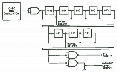
Fig. 9-24. Tunable oscillator.
Fig. 9-25. Suggested dial layout.
Wire the VFO portion using point-to-point technique on insulated standoffs. The divider is on perfboard and wired with wire-wrap pencil.
Summary. While this unit is just the basic generator, additions might enhance its operation. Some of the possible additions and their applications include the following:
• FM the VFO with an audio oscillator and voltage variable capacitor for working with FM receivers, phase detectors or PLL circuits.
• Switch the divider chain from the internal VFO to an external input jack. This would allow signals from external sources to be divided.
• Switch the divider chain input between the internal VFO and a crystal oscillator to generate harmonically-related standard frequencies.
Fig. 9-26. Oscillator.
• Add a second buffer and output circuit for opposing polarity outputs.
• Run the output through a one-shot multivibrator for thin-line pulse generation.
In case you use this as an rf generator for general purpose work, you might be interested to know that the square wave output generates strong harmonics beyond 2 meters!
Bargain Audio Frequency Source
About a month ago one hobbyist had occasion to check the frequency response of an audio filter he had built. Unfortunately, his modest test bench lacked an audio oscillator. He had been unable to complete several projects because he didn't have such an oscillator. Buying one was out of the question. Being a college student, his financial status was only slightly above that of a medieval serf.
One day while visiting a local Radio Shack, he walked by the record rack and looked over the selections. All of a sudden there it was-a solution to the audio oscillator problem. In the corner of the rack sat Stereo Test Record ... number 50-1971, which, in addition to many stereo system tests, contained twenty different test tones. It was only $ 1.49.
Fig. 9-27. Power supply circuitry.
Fig. 9-28. Dividers and output circuit.
Inside of an hour, he had checked out the record on a friend's oscilloscope, which showed that the tones were pretty much sinusoidal. A little work with pen and paper showed that, if played at different speeds, the record could produce 71 unique tones. Granted, the record is hardly a replacement for a good oscillator, but it's certainly great in a pinch. It can even be used for checking the approximate bandwidth of phase-locked loops.
Table 9-7 lists the frequencies, to the nearest cycle, which can be generated when the record is played on a four-speed turntable.
The Audio Synthesizer for RTTY, SSTV and Whatever
Have you ever had a need for an audio generator for precisely tuning your SSTV or RTTY equipment? This audio frequency synthesizer generates highly accurate tones useful for tuning both SSTV and RTTY station equipment. The output frequencies are within . 4 Hz of the exact desired frequency of eleven tones critical, or very helpful in the tuning of an SSTV or RTTY station. A single crystal is subdivided to derive the desired tones, and the complete unit can be built for less than $20. The frequencies considered critical to SSTV tune-up were 1200, 1500 and 2300 Hz, representing Sync, Black and White respectively. In addition, 1700, 1900 and 2100 were considered useful for grey scale adjustments of SSTV, so these were added, resulting in six synthesized frequency requirements for SSTV.
Table 9-7. Generated Frequencies.
*Actual turntable speed is 78.26 rpm.
**Beyond the capabilities of most phonographs.
RTTY has five frequencies which can be considered critical to tune-up.
These are 1275, 1445, 2125, 2295 and 2975 Hz. These are the five tones which may be utilized on either wide or narrow frequency shift keying, using the low or high tone set.
Theory of Operation. The af synthesizer starts off with a simple crystal oscillator feeding three synchronous binary counter ICs. Since each IC has four stages, a possible frequency division of 2 12 or 4096 exists before the counters carry to 4). However, if the proper outputs are gated together, the counters can be reset prior to 4096, thus establishing control of the exact frequency division. As shown on the schematic in Fig. 9-29, by sequentially labeling the outputs of the counters in powers of 2, the desired frequency division can be easily assembled. The problem then becomes one of getting the simplest gating combination for the desired accuracy.
A rather complex computer program was written to analyze the problem stochastically, and the relevant portion of the printout is shown in Table 9-8.
Fig. 9-29. SSTV and RTTY frequency synthesizer.
The computer did in a few minutes what would take years of manual calculation and comparison. Eleven NAND gate decoders are wired to detect a 1 bit at every input to produce a phi bit at the output of one of the decoders, the decoder of the selected frequency to be synthesized. This phi bit at the output of any decoder then produces a 1 bit at the output of the OR section, resetting the divider section and also toggling the output flip-flop.
The various NAND division decoders are selected by a switch which puts a + enabling voltage on one input of the desired frequency's decoder. If remote manual, or electronic selection is desired, such as a grey scale pattern for SSTV, or AFSK for RTTY transmission, the builder merely has to supply a + voltage to the desired decoder selector input in the sequence or for the time required.
Since the calculated frequency has been doubled, then halved in the output flip-flop, the output waveshape is a symmetrical square wave, excel lent for tune-up and calibration, but poor for transmission. If you wish to transmit this signal, build a low pass or bandpass filter to convert the output to a sine wave. Those not needing either SSTV or RTTY synthesis can omit the unneeded decoder NANDs, the 7430 or gate associated with the undesired block of decoders and the 7402. The remaining 7430 in the OR section is then directly connected to the 7473 and the Clear line.
Construction. One experimenter built the af synthesizer as a self contained unit having its own power supply. The cabinet is a Radio Shack #270-252 measuring 4" wide by 2- 3/8” high by 6" deep. The power trans former is any 12 volt AC 300 mA or more unit that you may have around.
The actual IC board is a perfboard unit with . 1" center holes measuring 2 1/2" by 4 1/2 ". The ICs and other parts are inserted and then the tedious wiring with #30 wire and a small, fine tipped soldering iron begins. Since it is very easy to make a mistake, be sure to develop some kind of a wiring system, such as labeling the ICs and wiring similar sections sequentially.
It is easier to build if an ordered process is followed which will allow progressive testing. Complete and test the power supply first. Next wire up power pins of all the ICs and build the crystal oscillator. After you have verified proper oscillation, wire up the three frequency dividing ICs, and temporarily ground pin 14 of these three ICs. Look at pin 7 of the last 74193 with an oscilloscope. If everything is working correctly so far, you should see a square wave, 1593.75 Hz in frequency.
Start wiring the decoders by wiring the 7430 labeled "1200". Reading the abbreviated schematic in Fig. 9-29, you will find that the 1200 Hz decoder requires a 2048, 512, 128 and 32 bit input to pins 2, 3, 4 and 5 respectively. The 2048 and 512 bits come from pins 7 and 2 of the third 74193, and bits 128 and 32 come from pins 7 and 2 of the second 74193. Pin 1 of the 1200 Hz decoder is connected to "A" (the 1200 Hz position of the switch). The output of the 1200 Hz decoder (pin 8) is connected to the 7430 OR gate NAND associated with the SSTV frequencies, the 1200 Hz decoder input, pin 1.
Then wire the other connections to the OR section, except do not connect the OR inputs to the unwired decoders yet. Remove the temporary ground from pin 14 of the 74193s and connect the OR section output as shown on the schematic to the pin 14s of the 74193s and the input pin of the output 1/2 7473.
Select 1200 Hz on the switch, and the output of the synthesizer should now read 1200 Hz, ± one digit, on a frequency counter. Now wire the rest of the frequency decoders and test each one. If any selected output does not read out correctly on the counter, you either have an error in your wiring, or a defective IC. Or maybe a bum counter! Extending/Modifying The Af Synthesizer. The unit can also synthesize other frequencies between 800 Hz and 3264 kHz with varying degrees of accuracy. The lower the desired synthesized frequency, the greater the ...
Table 9-8. Computer Printout of Frequency Synthesis Combinations.
... probability that the resultant output will be very close. A number of extra, currently unused, input gates in the OR section are shown on the schematic.
These can be connected to additional decoders, and additional switch positions will allow selection of up to 16 synthesized frequencies.
Suppose you wish to add 1000 Hz output. First use the following formula to derive the frequency division needed:
3264000 / Division required - Synthesized Frequency Desired
Entering our desired frequency of 1000 Hz we get:
26 = 3264000 34 1000
Next, we determine the binary divisions required. Sequentially sub tract the highest binary number listed on the 74193 outputs, in descending order:
3264 - 2048 = 1216 - 1024 = 192 - 128 = 64 - 64 = 0.
This indicates that a decoder connected to the 2048, 1024, 128 and 64 outputs of the 74193s will give a 1000 Hz synthesized output from the af synthesizer when selected.
A problem comes in when the division required is not a whole number.
In this case, the division required is rounded off to the nearest whole number, but some resultant inaccuracy will have to be tolerated, or a new computer analysis can be run, using this new desired frequency as another simulation constraint.
Table 9-8 shows several examples of how the computer listed the resultant error for this hobbyist. The first number on the top line was the stochastically selected master frequency. The SSTV and RTTY frequencies required the 11 division ratios shown to the right of the master frequency. 2100 Hz actually required a division of 1554.29. The computer rounded off to 1554 beneath, and then calculated the resultant frequency and the required binary divisions. Notice that the 1554 division results in a frequency 0.3861 Hz too high, but this is close enough for this application so the design was accepted.
Another consideration is that a 7430 has only eight input legs. Since one input goes to the switch, each decoder must use a maximum of seven input legs to the counters. This was another variable entered into the computer as a design constraint. Note on the printout of Table 9-8 that only one decoder (1900) required all eight inputs. Synthesized frequencies requiring only two counter inputs can use a 1/2 7410 as shown, and those requiring only three can use a 1/2 7420, in the interest of lowering the total IC count.
Conclusion. This project has presented an af synthesizer for SSTV and RTTY frequencies which is accurate to within . 4 Hz, in the worst case. A computer was utilized to obtain the needed data for building a unit which gives the required accuracy, as well as minimizing the complexity of the unit.
The output is a symmetrical square wave.
Build an Amazing Function Generator
The increasing popularity of a relatively new piece of test equipment (the function generator) has spurred at least two IC manufacturers to design special monolithic chips for this purpose. The Intersil 8038 and the Exar XR2206 are examples of such specially committed ICs. These new ICs offer great simplicity in function generator construction, but offer the user very little feel for what is actually going on in the process of waveform generation.
Since the building of a piece of test gear is also a learning process, circuit flexibility and stage-by-stage analysis are important. For this reason, an older design for a function generator from a Motorola application note (AN510A) was the starting point for this project. The original AN510A output amplifier section is a real klooge by today's standards, and so it was replaced by a simpler all-IC substitute. The original power supply used two dual-winding power transformers, four integrated bridge rectifiers and four power IC regulators. This rather elaborate supply was replaced with one inexpensive transformer, one integrated bridge rectifier and two of the newer Raytheon ± regulator ICs. A feature in the new function generator is DC offset, a simple addition that is really worthwhile.
The circuit of the function generator is shown in Fig. 9-30. Note that four ICs as well as a number of discrete devices are used in the wave-forming circuitry. In addition, two more power ICs are used in the power supply, shown in Fig. 9-31. A block diagram of the wave-forming circuitry is shown in Fig. 9-32.
The integrator is composed of U1 and Q1; an op amp and an emitter follower to lower the op amp output impedance.
The comparator is composed of U2, Q2, Q3, Q4, Q5, Q6, Q7, D8 and D9. U2 is an Emitter-Coupled Logic IC capable of extremely fast switching.
Associated with, but not actually part of, the comparator are D10, D11 and D12 which serve as voltage regulators to provide U2 with +1.4 volts and -3.9 volts. It is worth noting that Q4, Q5 and Q6 were originally designated as Motorola MPS-L08 types in AN510A, but since this transistor type is now obsolete, appropriate substitutions have been made.
The reference switch is made up of D1, D2, D3 and D4. Note that D3 and D4 are dual diodes. Also note that RB in Fig. 9-32 is either R8 plus R10 or R9 plus R11, depending on the state of the reference switch.
Fig. 9-30. Function generator, waveform circuits. CI- 10,•F 50V NONPOLAR (
MYLAR.ETC C2- 1,.f • C3-0.I..F • • C4-0 01,.F • • C5-1000PF • • C6-100pF
• RESISTORS ARE 1/4vi a 5% UNLESS NOTED
Fig. 9-31. Regulated power supply for function generator.
The sync amplifier is a simple differentiator, rectifier and emitter follower. The square wave from the comparator is differentiated by C13 and R30. D7 allows only the positive-going spike to be passed to the base of Q8.
This positive spike is then available at the emitter of Q8 for a sync pulse.
The sine wave shaper consists of D5, D6, Q9 and Q10. D5 and D6 act as soft clippers on the triangle wave, and produce a near approximation to a sine wave. Q9 and Q10 simply act as emitter-followers after shaping-one NPN and one PNP, so that their emitter-base voltage drops cancel each other.
Since it was necessary to attenuate the triangle wave (with the voltage divider R33-R34) to make it compatible with the shaping diodes D5 and D6, the resulting sine wave is smaller in amplitude than the triangular wave or square wave. To equalize the output levels of the three waveforms, simple "T" attenuators are placed in the triangle and square wave lines. These consist of R38, R39, R40 and R41, R42, R43 respectively.
Finally, the output amplifier consists of U3 and U4, a high slew-rate op amp and buffer amplifier. Note that the buffer is inside the closed loop of the amplifier. By adding in variable DC at the inverting input of U3 via a 120k resistor, a "DC offset" adjustment is easily obtained. This DC offset enables one to offset the three types of waveforms for testing of circuits which will accept only unipolar signals, such as logic circuits.
The power supply utilizes a Triad F4OX (26.8 Vct 1A) transformer which combines low price, small relative size and high current capability. An integrated bridge and two Raytheon RC4194TK integrated circuits in the circuit of Fig. 9-31 provide -± 15 volts and -.±6 volts for the wave-forming circuitry. The RC4194TKs are heat-sink mounted to the chassis with T066 mica wafers for heat transfer and electrical insulation. The F4OX trans former is mounted under the chassis to keep it electrostatically shielded from the top-mounted waveforming circuits. The two 1000 uF filter capacitors are also mounted under the chassis because of the relatively large AC line ripple on them.
The function generator is built into an old 7" x 8" x 10" steel equipment cabinet, to which an aluminum panel has been fitted. The aluminum panel was originally an old black-crackle finished relay rack panel which was stripped of paint and cut down to size. The left over portion of this same panel was made into the frequency dial, by rough sawing and turning down the outer diameter on a lathe. The large aluminum spinner knob for the center of the frequency dial was also turned from a scrap of bar stock on the lathe. The basic planetary drive for this control was a National Velvet Vernier salvaged form a surplus BC375 or BC191 tuning unit. Those with fancier dial systems available or without access to a lathe and the above surplus drive units can use other methods-even a plain large knob. One will note that the timing capacitors in the circuit of Fig. 9-30 is a 10 uF non-polar type. An old 10 uF 600 V transmitting capacitor was used. It was mounted on a homemade insulating mount, as otherwise stray capacity to the capacitor case was objectionable in this circuit.
The relatively small amount of circuitry of the power supply is mounted under the chassis. The power supply should be the first section checked out, preferably before connecting it to the waveforming circuits. Note that each RC4194TK has a 71.5k resistor from "case" to #3. This is the nominal value suggested by Raytheon. Sorting through one's 68k and 75k resistors will
Fig. 9-32. Block diagram of function generator.
------------
Table 9-9. Parts List.
D1,2 -Silicon signal diodes: Motorola MSD6102, 1N4454, or 1N914
D3 -Dual Si. signal diode: Motorola MSD6150, or two 1N4454, 1N914
D4 -Dual Si. signal diode: Motorola MSD6100, or two 1N4454, 1N914
D5-9 -Silicon signal diodes: Motorola MSD6102, 1N4454, or 1N914
Q1, Q8, Q9 -NPN Xstr: Motorola 2N4124 or HEP53, or 2N3643, or HEP- S0014
Q2, Q3, Q7 -NPN Sw. Xstr:Motorola 2N709 or HEP50, or 2N3646, or HEP- S0011
04, 05, 06 -PNP Sw. Xstr:Motorola 2N4260 or HEP720, or 2N3640, or HEP- S0019
Q10 -PNP Xstr:Motorola 2N4126 or HEP57, or 2N3644, or HEP- S0019 U1 -Motorola MC1420G or MC1520G U2 -Motorola MC1035P or MC1235L U3 -National Semiconductor LM318H, LM218H, or LM118H U4 -National Semiconductor LH0002CH or LH0002H D10 -Mototola 1N4730A or HEP- Z0403 D11, 12 -Motorola 1N4001 or HEP- R0050
---------------
... give a few values close to 71.5k. Use these. The 37.5k and 15k resistors from pin #2 of the RC4194TKs will then be target values to give ±15 volts and ±6 volts respectively. Some juggling of these target resistance values may be required to give exactly the voltages desired.
Assuming that the power supply has been checked out, as above, and puts out ±15 and ±6 volts, the waveforming circuitry can be connected to it.
The pots R1, R8, R9 and R19 should all be set at mid range, and the pot R21 set at minimum. The DC offset pot should also be set at mid range.
With the scope on the wiper arm of R19, adjust this pot until the waveform looks like a square wave (i.e., the positive portion is as long as the negative portion). Then put the scope on the emitter of Q1, and adjust R8 and R9 until the triangular wave observed there has a ±2 volt value. R19 should be re-tweaked and then R8 and R9 again. The scope can now be shifted to the output, and DC offset, level, frequency and sine-shaping checked.
This function generator is a useful piece of test equipment built up from odds and ends. While the semiconductor costs can be as high as $35.00, appropriate substitutions can trim this figure somewhat. To this end most of the diode (D) and transistor (Q) designations have several acceptable numbers given in the parts list of Table 9-9.
Build This Simple Noise Generator
For several years, there have been quite a few noise bridges available.
The noise generators are all based on the use of noisy diodes (usually a 1N753, 6.8-volt zener, back biased) which go through two or three stages of transistor amplification and then into the various configurations of bridges.
They all do a creditable job, but they use a great number of components and draw too much current. A noise bridge is a must for mobile operation, where the mobile antennas have a high Q and should be operated at very close to resonance. Using a bridge, you can QSY quickly and readjust the top section of the antenna for exact resonance. Plus or minus 10 kHz is about the tolerable excursion. A transistor version of a white noise generator was built and tested.
The results were superior to any of the systems tried with a noise diode.
Some diodes were so noisy that little amplification was needed; others made so little noise that even three stages of amplification were not enough, to say nothing of the undesirable added current consumption.
How does this circuit generate such a wide band of frequencies? This oscillator may. be described as a self-quenching device which is capable of generating square wave pulses with nearly ideal square wave. We know that a pure sine wave does not contain any harmonics. A sine wave with some distortion generates some harmonics. A perfect square wave generator will produce its fundamental frequency plus all the higher frequencies to infinity.
With the materials used to produce this perfect square wave, we find that the usable bandwidth is actually far short of infinity. Tests indicate that the usable noise frequency is from somewhere around 500 kHz to far beyond 30 MHz, the amplitude remaining quite constant over the entire bandwidth.
Oscillation starts at 1 1/2 to 2 volts and continues at a nearly constant level on all the HFs up to 20 volts. At 3 volts, the current drawn is about 200 microamps. At 20 volts, the current drawn is about 6 milliamps. This is ideal, whether you want to use the bridge with two AA cells, a 9-volt transistor radio battery or 13 volts from your car battery.
Several types of NPN transistors, high gain and in metal can or plastic, were tried. Most of them worked. However, it was found that 2N2222 transistors are the most easily obtained. They are cheap, also.
There are three components that must be given special notice. They are the RFC, the number of turns on the toroid and the manner in which they are wound and the disc ceramic capacitors. The 0.01 disc capacitors must be the 1,000-volt variety. Several dozen units have been built and sold with no problem, with these precautions taken.
The RFC consists of 24 to 26 turns of enamel #26 to #30 wire wound on a form about 4 to 6 mm (3/16" to 1/4 ") in diameter and about 17 mm long (11/16"). The form to hold the wire may be any reasonable good insulator, such as a plastic knitting needle or a piece of #8 house wire with the wire removed from the plastic insulation and a wooden match stick inserted in place of the wire to make it rigid. A 1/2 - watt ohmite-type of resistor, more than 100,000 ohms, also worked fine.
The toroid coil is wound on a T-50-2 (red mix) core. The core is rated for use between 500 kHz and 30 MHz.
Fig. 9-33. PC board-actual size.
For the primary winding on the core, which will connect to transistor collector and to the positive voltage, wind 24 turns as follows: Hold the toroid in your fingers, in a horizontal plane, and make the first turn with the starting end of the wire sticking up out of the core about 5 cm (2"). Now make the first turn so that the long end of the wire will come out of the toroid on the right side of the starting wire. The next turn will come out of the toroid on the left side of the starting wire. The completed primary winding will have a bundle of 24 turns, or 12 turns on each side of the starting wire.
By doing this, we have a coil with minimum stray capacitance coupling between primary and secondary.
The secondary, or output winding, will be 12 turns of bifilar, wound and connected to give a total of 24 turns. Cut two pieces of the same enamel wire about 40 cm (16") long. Put two ends together in a vise, and twist them about one twist per com (2 1/2 twists per inch). Wind 12 turns on the toroid, leaving about 5 cm (2") of wire out of the toroid on both ends. Use a pocketknife to carefully remove all the enamel far enough back toward the toroid so that you can cut off the excess length not needed for making the connections to the coax connectors, bearing in mind that the two outside ends of the winding should be exactly the same length.
Select a wire from each end of the winding and test with an ohmmeter to find two wires that do not show continuity. Connect those two wires together. Now you should test to make sure that you do have continuity on the remaining two wires. This gives you the two bifilar windings in series, with a center-tap, or 24 total turns. Adjust these windings on the toroid core so that the primary and secondary windings have equal spacing between the two coils on both sides.
The toroid core with its windings should be mounted on a small plastic or wood pillar about 2mm ( 5/8”) long and cemented on the PC board. The white silicone cement available at nearly any store is ideal for this purpose.
Refer to the PC board layout in Fig. 9-33. Follow the pattern quite closely and all the parts will fit nicely into place. The values of all the components are indicated in Fig. 9-34. The diagram showing the Rx pot, the 360 pF variable capacitor, the 180 pF fixed capacitor and two coax connectors should be studied and used as a guide for making it a balanced system.
That is, the lead lengths of the fixed 180 pF capacitor should be the same length as the lead of the 360 pF variable where they connect to a solder lug at the detector (DET) output coax fitting. The lead to the 100-ohm ohmite pot should be as short as possible. The PC board is shown actual size, and it may be used as a template to make small punch marks on the copper foil.
--
Next: Frequency Counters