AMAZON multi-meters discounts AMAZON oscilloscope discounts
The device used most widely for both AC and DC power control is the PNPN switch known as the silicon-controlled rectifier, or SCR. It has many industrial-electronic applications, such as reversing and speed control for DC motors. In fact, it is rapidly replacing the thyratron tube for this and similar power control applications.
Silicon-controlled rectifiers can be considered in many ways as the semiconductor equivalent of thyratron tubes. SCR's have a higher efficiency than thyratrons because the voltage drop across an SCR is approximately 1.5 volts or less, as opposed to about 15 volts for a thyratron. Hence, there is a tenfold reduction of power loss for a given load current. Also, flashover and arcing problems are reduced because no electron tubes are used, and there is far less heat dissipation. Moreover, equipment using SCR's needs no time delay in starting, because SCR's have no filaments.
In addition to its anode and cathode, the SCR has a gate. By controlling the phase of the gate signal with respect to the phase of the supply voltage, the firing (delay) angle of the gate can be held to any point in the cycle up to approximately 180°. Through control of the firing angle, the average power delivered to the load can thus be controlled. The magnetic trigger, a special magnetic amplifier with a controllable firing angle, is a useful device for firing the gate circuits of SCR's.
The controlled switch is a PNPN device related to the con trolled rectifier. The controlled switch (CS) is similar to the silicon-controlled rectifier (SCR) in physical construction, theory of operation, and circuit applications. The CS, however, has a much greater firing sensitivity and is therefore useful in many low-level input applications not within the capability of the controlled rectifiers.
With an AC voltage source, the CS acts as a controlled half wave rectifier, since it will block both the positive and the negative half-cycles until a positive control signal is applied to the gate. As long as the control signal is present, the CS will then conduct during the positive half-cycle and block during the negative half-cycle. When the control signal is removed, the CS will block both half-cycles again, since it automatically turns off at the end of each positive half-cycle. By proper timing of the applied control signal, the CS can be made to conduct for all or part of the positive half-cycle. Thus, proportioning control of the output, as well as on-off switching, is possible.
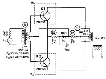
---------- Six-watt servo amplifier.
SIX-WATT SERVO AMPLIFIER
This six-watt servo amplifier has a frequency range of 40 to 40,000 hz using 2Nl658 transistors, and provides a power gain of about 30 db. Mica insulating washers and heat sinks ( aluminum plates 5" x 5" x ½ /') are used. Both sides are in free air. Transformer T1 is a UTC SSO-14 or equivalent with a secondary DC resistance of 22 ohms and a secondary voltage of 6.8 volts rms, end to end. Primary voltage is 50 volts rms end to end, and primary current is 2 ma rms. R1 is 5 ohms ± 10%, 5 watts; and R2 is 1,000 ohms + 10%, 2 watts.
D1 is a 1N91 or equivalent alloy-junction germanium diode.
C1 is approximately 5.2 mfd, although this value varies with the_ motor design. This capacitor is used to correct the power factor of the motor-control field to unity under locked-rotor conditions.
The two-phase induction servo motor is a Size 15 rated at 400 hz, 6 watts per phase. Its control field is designed for 35 or 36 volts rms, end to end. Re is the approximately 1,500-ohm output impedance of a 400-cycle generator.
The amplifier operates in a Class-AB mode because of diode D1, which also maintains the quiescent current at a constant value over the entire temperature range. With the power factor of the control winding less than unity under locked-rotor conditions, the motor will have a tendency toward single-phase operation, and the power output of the amplifier will be lowered.
(A) Load current with switch closed. (B) Load current with switch open. (C) Load current with switch open.
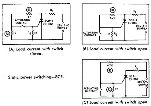
-------------- Static power switching-SCR.
STATIC POWER SWITCHING
Semiconductor-controlled rectifiers are often used where a large amount of power is to be switched, but the contact current and voltage must be kept low for simple and reliable operation.
The silicon-controlled switch (CS) or silicon-controlled rectifier ( SCR) provide a solution to this common control problem. Both are PNPN transistors. The sensitive actuating contacts need sup ply only the gate firing power, which can be as low as 50 microwatts ( 1 volt, 50µ a). The CS or SCR will directly provide up to 100 watts or more for the output load.
Three simple arrangements for switching power to loads are shown. The circuit in Part A of the diagram will provide load power when the actuating contact is closed, but not when it is open. The circuit in Part B provides the reverse of this action; power is supplied to the load only when the contact is open. If desired, both circuits can be made to "latch" by operating with DC instead of the AC supply indicated. In Part A, voltage divider R1-R2 provides the AC gate signal. In Part B, a closed switch causes the gate and anode to have the same potential; hence, the SCR will not fire.
In both circuits, the voltage across the sensitive contacts is under 5 volts, and the contact current is below 5 ma.
Contact current in Part C is almost tripled, but proper triggering of the SCR is assured. If desired, the contact current can be held well below 1 ma if a controlled switch such as the 2Nl877 ( 3A61) is used in place of the SCR. Also, R1 and Re can be larger in value because the firing-current and -voltage requirements of the controlled switch are significantly lower.
TIME-VARIABLE SCR CONTROL
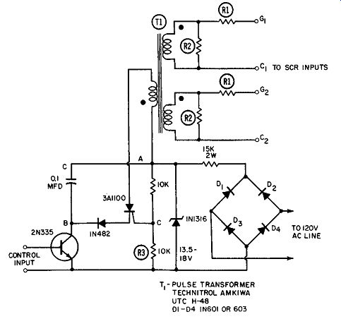
----- (A) Time variable control circuit for firing SCR.
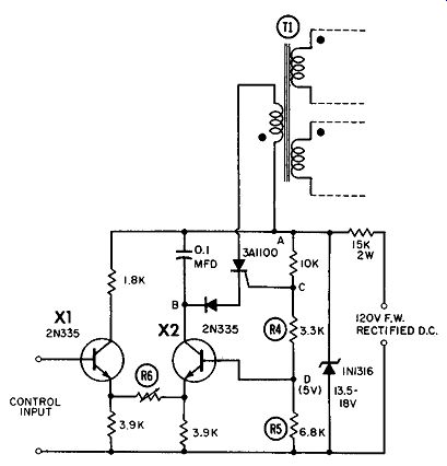
------------ Time-variable SCR control. (C) Control circuit with. balanced
input amplifier. (B) Output waveforms.
The preferred method of firing controlled rectifiers is to use a high-energy pulse. For most accurate timing, the pulse should have a fast rise time (0.5 µ.sec or less). It is unnecessary, and sometimes undesirable, to use a continuous gate signal. The reason is that when the SCR is conducting in the forward direction, its dissipation increases without contributing to the performance of the device. When the SCR anode voltage is negative, a positive gate signal substantially increases leakage current and therefore the dissipation. Pulse firing prevents these two un desirable conditions.
A time-variable pulse generator designed for firing high- as well as low-power SCR's is shown in Part A of the diagram. This circuit will deliver 5-volt, 200-ma pulses of 6 µ-secs or longer.
Pulse-transformer output isolates the two SCR's being triggered.
As shown, the circuit is designed for 60-cycle operation. Control is achieved from approximately 10° to 180° of the AC half-cycle.
Since the circuit consumes very little power, a subminiature zener diode can be used. The 15K current-limiting resistor has the highest dissipation, which is approximately 0. 7 watt at 120 volts AC. A 2N335 silicon transistor controls the charging current to the 0.1-mfd capacitor, and also provides electronic control of the time delay. Since the transistor is a constant-current device, the charging: rate is linear, not exponential. The time delay for firing is inversely proportional to the controlling input current at the base of the 2N335 transistor. A variable resistor can be used in place of the transistor if manual control is desired.
The circuit operation is as follows: AC line voltage is rectified by the D1 through D4 portion of the bridge circuit so that pulsating DC is obtained at point A. The 2N1316 zener diode and the 15K resistor limit the voltage at point A, as shown by the square waveform of Part B. A divider, consisting of two 10-K resistors, supplies a bias voltage equal to half the zener voltage to the gate of the 3Al6.
At the beginning of each half-cycle, capacitor C is discharged, and the voltage at point B is equal to the zener voltage. Thus, the cathode of the 3Al6 is positive with respect to its gate, and the CS is biased off. The 2N482 diode is also reverse-biased to minimize loading effects on the timing capacitor and to prevent exceeding the cathode-gate voltage rating of the 3A16. As the collector current of the transistor charges the capacitor, the voltage at point B drops toward zero. When it falls below the fixed bias on the gate by an amount sufficient to fire the 3A16, the CS will turn on, discharging the capacitor into the pulse-transformer primary.
If, for any reason, the capacitor does not charge sufficiently to fire the CS before the end of the half-cycle, the CS will fire when the voltage at point A drops toward zero at the end of the half cycle. When the voltage at point A drops to zero, the gate bias voltage for the 3A16 will also be zero. However, with the capacitor partially charged, the voltage at point B goes negative, causing the CS to fire and discharge the capacitor. Timing for the next half-cycle therefore starts with the capacitor discharged.
It is desirable to apply the AC voltage for the control circuit directly across the SCR's being controlled. This removes the sup ply voltage from the control circuit after the SCR fires, and thereby eliminates unnecessary dissipation in the control circuit.
The impedance reflected into the pulse-transformer primary should be low ( 20 to 50 ohms) and primarily resistive. Termination of the secondary windings as shown in Part A is desirable.
The input impedance of the rectifier being controlled will affect the termination.
For low-power units, R1 and R2 should be 100 ohms. High power units such as the C35, which require a relatively high firing current, can be driven directly from the secondary windings.
Series resistance of the pulse-transformer secondary windings will provide the necessary decoupling, without the need for R1 and R2. The 0.1-mfd capacitor should be replaced by a 0.2-mfd unit to furnish the higher energy requirements of high-power SCR's.
The circuit in Part C is the same as in A except that the single control transistor is replaced by a pair of 2N335 transistors connected as a balanced input amplifier. R2 in A is replaced by voltage divider R4-R5, which provides a reference of 5 volts to the base of X2. The balanced amplifier is self-compensating for temperature variations of transistor parameters.
The two 3.9K resistors in series with the emitters of X1 and X2 act as constant-current sources, establishing the total emitter current of both transistors at approximately 2 ma. With a control input voltage of 5 volts applied to the base of X1 ( the same as the reference voltage applied to X2) the two transistors share equally the total available emitter current of 2 ma. X2 provides a charging current of 1 ma to the 0.1-mfd capacitor. Under this condition, R6 has no effect on the circuit, since the current through it is zero.
When the control input voltage is raised above 5 volts, X1 re quires more current, taking it from X2 through resistor R6. When the control voltage is below 5 volts, the current through X1 is reduced and the charging current through X2 increases. The center of the proportioning-control voltage range is established by the reference voltage applied to the base of X2. A zener diode or any other voltage reference may be used in place of the simple voltage divider if greater reference stability is required.
Resistor R6 controls the gain of the balanced amplifier and can also be used to adjust the proportioning-control voltage range above and below the 5-volt center. When R6 is zero ohms, gain is maximum. Pulse delay is approximately 10° ( almost full output) when the control input voltage is 4.9 volts, and 170° ( almost no output) with a 5.1-volt input. Thus, a 4% input-voltage change can control the SCR from essentially zero to full power output.
Increasing R6 reduces the gain and broadens the proportioning range without altering the range center.
In the control circuit shown in Part C, an increase in control voltage decreases the power output. By applying the reference voltage to the base of X1 and the control input to the base of X2, the control sense can be reversed if desired.
---------------77 T1,T2,T3 ,= 2N696 OR 2N1613 T4,T5 •2N699
TWO-WATT SERVO AMPLIFIER
This servo amplifier has a gain of 1,000 and an input impedance of more than 10-K ohms. It operates over an ambient temperature range of -55°C. to +125°C, and has a continuous power output of 2 watts.
The first three stages are direct-coupled in order to reduce the number of time constants. This increases the phase margin for use in gain-stabilizing feedback. Direct coupling has the additional advantage of permitting a large bias resistor for X1 in order to increase the input impedance while retaining operating point stability by DC generation.
X3 is transformer-coupled into the common-collector output pair consisting of X4 and X5. Center-tapped operation utilizes the positive temperature coefficient of the motor winding to stabilize the quiescent operating point of X4 and X5.
AC SWITCH FOR THE SCR
Two circuits are shown for the C35 controlled rectifier. This C35 SCR is a three-junction semiconductor for use in power-control and power-switching applications requiring blocking voltages of up to 400 volts and load currents of up to 16 amperes. Series and parallel circuits may be used for higher power applications.
The CR reverse characteristic is similar to that of a normal silicon rectifier, in that both represent essentially open circuits with a negative anode-to-cathode voltage. The forward characteristic is such that it will block the positive anode-to-cathode voltage below a critical breakover voltage if no signal is applied to the gate terminal. However, by exceeding the forward breakover voltage or applying an appropriate gate signal, the device will rapidly switch to a conducting state and present the characteristically low forward voltage drop of a single-junction silicon rectifier.
Part A shows a simple series switch S, which applies an AC signal to the gate. R limits this gate current to a safe value, and the diode prevents the application of inverse voltage between the gate and cathode during the nonconducting cycle. Load R can be of any value within the limits of the SCR. For the C35 series, the maximum current is 16 amperes average at a forward drop of less than 0.9 volt.
As long as S is open ( Fig. A), the SCR will not fire when AC is applied. Closing S allows the positive alternation to cause conduction, since the gate fires the SCR and its anode is positive.
As shown in Part B, the SCR fires for 135° and will not fire on the negative alternation. Thus, closing S will control the firing point for each positive alternation, and DC current will flow through the load.
It is possible to use DC on the gate to control the firing point.
Or, as in Part C, the circuit can be fired by opening S where the switch is from the gate to the cathode.
In circuit A, the load current can be interrupted by opening S or by the negative anode voltage. In B, the load current can be interrupted by closing S or by the negative anode voltage.
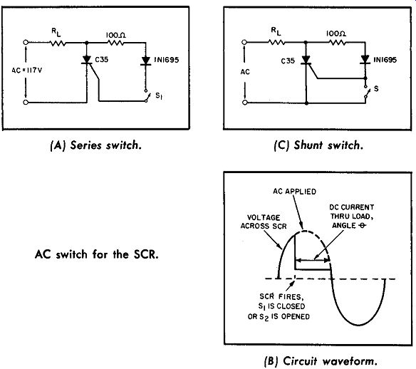
--------------- AC switch for the SCR. (A) Series switch. (B) Circuit waveform.
(C)Shunt switch