AMAZON multi-meters discounts AMAZON oscilloscope discounts
Timing circuits have an important place in industrial electronics. Applications range from delay elements which permit large power tubes to heat up before the anode supply is applied, to a sequential-circuit control for use with welders. Sweep circuits like those in oscilloscopes, sweep-signal generators, or light flashers are, in a sense, also timing circuits.
One can divide timers into two circuit elements-active ( such as the tunnel diode, transistor, or unijunction), and reactive ( usually a capacitor, although it could be an inductor). In an RC circuit, for example, a capacitor charges exponentially through a resistor. At some point along the charging curve, the voltage across the capacitor is sufficient to fire the active element and produce an output. In this way, various time periods may be produced as different values of capacitance are switched into use.
For more precise timing, a stable oscillator can be used as a signal source. By clipping and differentiating, pulses can be produced; if these are counted in a digital fashion, quite accurate timing can be accomplished.
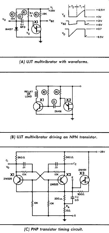
-------------- (A) UJT mu/tivibrator with waveforms. (B)UJT multivibrator driving
an NPN transistor. (C) PNP transistor timing circuit.
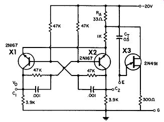
-------------- (D) NPN transistor timing circuit.
above, a-d: UJT timer circuits.
UJT TIMER CIRCUITS
Unijunction transistors (UJT) are useful as timing switches in transistor circuits. Part A shows a unijunction-transistor multivibrator circuit with a frequency of about 1 khz. The length of time the unijunction transistor is off ( no emitter current flowing) is determined primarily by the value of R1, while the value of R2 determines the UJT "on" time.
An NPN transistor may be direct-coupled to the multivibrator by replacing the diode, as shown in Part B. The advantage of this circuit is that the load does not affect the timing of the multi vibrator.
The unijunction transistor can be used in conjunction with conventional PNP or NPN transistors to obtain versatile timing circuits such as symmetrical and unsymmetrical multivibrators, one-shot multivibrators, variable-frequency oscillators, and time delay circuits. The advantages of these circuits include: ( 1) the output at the collector of each transistor is nearly an ideal rectangular waveform, ( 2) the circuits will tolerate large variations in transistor characteristics, ( 3) the circuits are not prone to "lock-up" or non-oscillation, ( 4) the timing stability is excellent, and ( 5) a single small timing capacitor can be used, avoiding the need for electrolytic capacitors in many applications.
The hybrid timing circuits can use either germanium or silicon transistors. Basic circuits using PNP and NPN transistors are shown in Parts C and D. In both of these circuits, the junction transistors form a conventional flip-flop, with the unijunction transistor serving the timing and triggering functions. Each time the unijunction transistor fires, the discharge current from capacitor CT develops a pulse across RA which triggers the flip-flop from one state to the other. The basic circuits will operate at frequencies from about 1 hz to 500 hz and at temperatures above 75°C. Frequencies from 1 cycle per minute to 100 khz can be obtained by proper choice of CT and RA and by suitable flip-flop design. The operating-temperature range may be extended to 150°C. by the use of silicon transistors.
SAWTOOTH-WAVE GENERATOR
In this unijunction generator, NPN transistor X2 is in a state of conduction while the unijunction (UJT) is normally cut off. When a negative-going sync pulse is applied to the base of the UJT, the cutoff bias is overcome and the UJT conducts from +20 volts, through the 12K and 22K resistors, to ground via the UJT. Because of the UJT conduction, the increased IR drop across the 12K and 22K resistors will cut off transistor X at its base. X's voltage-going positive at the collector and negative at the emitter-is taken off at points A and B, as represented by the waveforms. Outputs A and B are 6 and 10 volts peak-to-peak, respectively, in a frequency range of 350 to 600 hz.
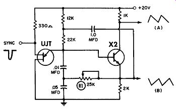
------------- Sawtooth wave generator.
STROBOSCOPES
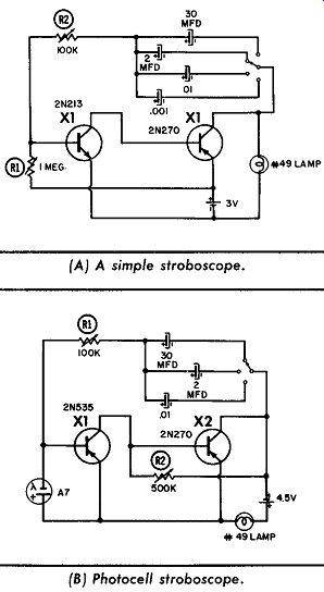
---------- Stroboscopes. (A) A simple stroboscope. (B) Photocell stroboscope.
Stroboscopes are light sources which, because they can be turned on and off rapidly, appear to stop motion. Thus, a motor turning at 1,200 rpm will appear to stand still if viewed under a light flashing 1,200 times per minute. A light flashing 1,199 times a minute will make the motor appear to rotate at 1 rpm. At 1,201 times a minufe, the light appears to cause a reverse rotation of 1 rpm. Among the many uses for stroboscopes is the measurement of frequency response of photocells.
From 10 through 6,000 sharp sine-wave flashes per second can be obtained on the four-range stroboscope shown in Part A. The 30-mfd selector-switch position is the low range. Increasing R2 increases the flash duration, and increasing R1 increases the period.
Another stroboscope design, shown in Part B, uses a photocell to receive the positive feedback from the output circuit and thereby provide the oscillatory flashes. The lamp must be mounted directly on the photocell ( or close to it) in order for the circuit to oscillate. Both designs make versatile stroboscopes out of ordi nary components.
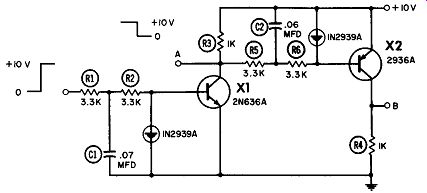
------------ Tunnel-diode time delay.
TUNNEL-DIODE TIME DELAY
In this circuit, a positive-going input signal across C1 and R1 will charge C1. When C1 reaches the avalanche rating of the tunnel diode, T D1 will conduct and apply the necessary bias to X1, which will now conduct. Thus there is a delay of about 120 microseconds between the input and output signals.
When X1 conducts, its collector voltage ( normally + 10 volts ) drops to a very low value. This negative-going voltage overcomes the bias of the other tunnel diode and causes conduction. Now that its forward bias has been established, transistor X2 can con duct. Thus, by adding an odd number of stages connected in a loop, it is possible to produce a multiphase oscillator.
TRIGISTOR DELAY TIMER
This circuit shows a one-shot multivibrator or delayed-pulse generator using a PNPN transistor ( Trigistor), which can provide accurate timing for delays of up to 10 seconds. The Trigistor characteristics have only a small effect on timing, and accuracy is determined essentially by the stability of the 10-mfd timing capacitor and the supply voltage. With the values shown, this circuit will provide a one-second rectangular pulse output.
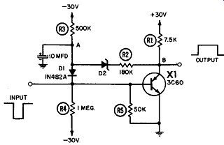
------------- Trigistor delay timer.
With the circuit in its quiescent condition, the Trigistor is on.
Point B is at 1 volt, and point A is at -11 volts due to the voltage divider action of R2-R3 and the 5-volt zener diode. The 1N482A is connected in the reverse direction. R4 and R5 provide bias stabilization.
When a negative trigger pulse is applied to the input, the Trigistor is turned off. Point B rises to about 30 volts, and the capacitor begins to discharge through R1, R2, and the zener diode. When point A reaches +L5 volts, D1 conducts and the Trigistor turns on, bringing point B back to +1 volts. The capacitor then charges through R3, back to its quiescent voltage of -11 volts.
INTERVAL TIMER WITH HIGH-LEVEL OUTPUT
Control circuits sometimes require a timer with a high-level output. Semiconductor-controlled rectifier SCR-1 in this circuit provides 1 ampere to the load for one second, using a 28-volt DC supply.
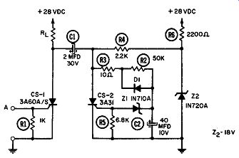
------------ Interval timer with high-level output.
The timing cycle is started by applying an input pulse to point A. (A 5-microsecond or longer pulse with a minimum amplitude of 1 volt is required.) This pulse turns on SCR-1, which in turn supplies power to the load. At the same time, SCR-2 is turned off by the action of commutating capacitor C1, and timing capacitor C2 commences to charge through R2, R3, and R4. Zener diode Z2, which is used to establish a fixed charging-voltage source, minimizes the timing error due to variations in the source voltage.
When the charge on C2 reaches approximately 7.5 volts, Z1 will conduct sufficiently to cause SCR-2 to fire. Using the values shown, this occurs one second after the initiating pulse, and the action of commutating capacitor C1 turns off SCR-1. Power is thus removed from the load. C2 discharges rapidly through diode D 1 and R3, so that total recycle time is less than 1 millisecond.
A short pulse thus turns on the power to the load for a period determined by C2 and its charging-path resistance. This technique takes advantage of the high current-handling capability of the controlled switch. In addition, the circuit can be actuated directly from a low-level pulse; because of the inherently high gain of the SCR, no intermediate amplifiers are needed.
UJT TIME DELAY
This figure shows a uni-junction transistor ( UJT) used as a time delay. When the switch is closed, the capacitor charges through RT until the UJT fires. The resultant current through the relay coil closes its contacts. A double-pole relay is often used so that one set of contacts will hold the relay closed while the other set is used for control. A fast-acting relay with low coil resistance is required.
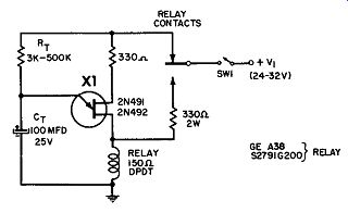
------------- UJT time delay.
The time delay is three seconds with an RT of 3K, and 500 seconds ( over eight minutes) when RT equals 500K. In other words, a delay of about one second is obtained for each thousand ohms of timing resistance.