AMAZON multi-meters discounts AMAZON oscilloscope discounts
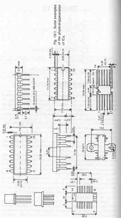
An integrated circuit, or IC, consists of a single-crystal "chip" of silicon on which has been formed resistors, capacitors, diodes, and transistors (as required) to make a complete circuit with all necessary interconnections; the whole lot in micro-miniature form, see Fig. 13-1. The cost of an IC chip is surprisingly low, considering how complicated it can be. This is due to the large quantities processed at a time. A 1-inch square wafer, for example, may be divided into 400 individual IC chips, each containing up to 50 or more separate components. As many as 10 wafers may be processed at the same time, yielding 4000 ICs containing the equivalent of nearly a quarter of a million components! Apart from the convenience of having a complete circuit in such a small size, ICs are very reliable because all components are fabricated simultaneously and there are no soldered joints.
Diodes and transistors in an IC chip are formed by exactly the same process used for producing individual diodes and transistors, but in very much reduced physical size. (Diode and transistor fabrication is explained in some detail in a companion volume by the author, Building and Designing Transistor Radios, a Beginners Guide.) Integrated resistors are much simpler. They can be a very tiny area of sheet material produced by diffusion in the crystal, or thin film (a millionth of an inch thick) deposited on the silicon layer. Practical resistor ranges which can be achieved are 10 ohms to 50 kilohms, depending on the actual construction, in an area too tiny to see with the naked eye.
Capacitors are a little more difficult. They can either be based on a diode -type formulation (diffused junction capacitor) or again be based on thin-film construction (MOS capacitor). Typical capacitor values achieved are 0.2 pF per thousandth of an inch area. Usual maximum values are 400 pF for diffused junction capacitors, and 800 pF for MOS capacitors.
Inductances are another story. They cannot--as yet-be produced satisfactorily on silicon substrates using semi -conductor or thin-film techniques. Hence, if a circuit specifically needs an inductance in it, the corresponding IC chip is produced without it and an individual inductance is connected externally to the IC.
This, in fact, is common practice in the application of many ICs. The IC is not absolutely complete.
It contains the bulk of the components, but the final circuit is completed by connecting up additional components externally. It is also usually designed as a multi-purpose circuit with a number of alternative connection points giving access to different parts of the circuit, so that when used with external components, connection can be made to appropriate points to produce a whole variety of different working circuits.

Fig. 13-1.
MONOLITHIC AND HYBRID ICs
Integrated circuits built into a single crystal are known as monolithic ICs, with the characteristic of incorporating all necessary interconnections.
The problem of electrical isolation of individual components is solved by the processing technique used.
In another type of construction, individual components, or complete circuits, are attached to the same substrate but physically separated.
Interconnections are then made by bonded wires.
This type of construction is known as a hybrid circuit.
MSI AND LSI
MSI stands for medium -scale integration; and LSI for large-scale integration, referring to the component density achieved. The figure of 50 components per chip has already been mentioned as typical of conventional IC construction. These fall into the category of MSI chips, defined as having a component density of more than 12 but not more than 100 components per chip. LSI chips have a much higher component density-as many as 1,000 components per chip.
This is largely due to the considerable saving in component sizes Possible using thin-film techniques instead of diffusion techniques, particularly in the case of transistors.
For example, an MOS transistor can be one tenth the size of a diffused bipolar transistor for the same duty. Hence many more components can be packed into the same size of IC chip.
OP AMPS
The operational amplifier or op amp is a type of IC used as the basic building block for numerous analog circuits and systems-amplifiers, computers, filters, voltage-to-current or current-to-voltage converters, modulators, comparators, waveform generators, etc. It is a typical, almost complete circuit, used in conjunction with a few external components to complete the actual circuit required.
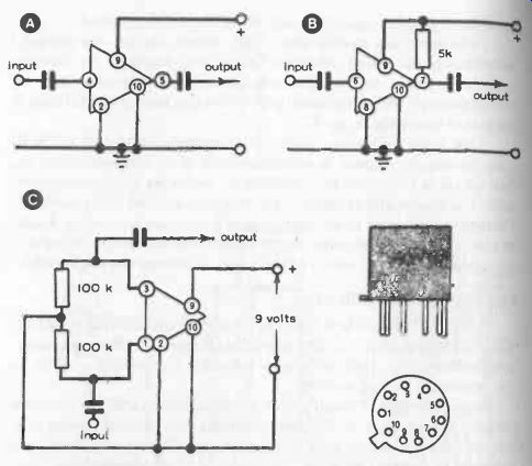
Three typical circuits using a simple op amp "chip" are shown in Fig. 13-2.

Fig. 13-2. Three amplifiers based on the CA 3035 IC, all giving a gain of
about 100. All externals capacitors are 10 uF.
A. Input resistance 2 k ohms
B. Input resistance 670 ohms
C. Input resistance 50 k ohms
D. Enlarged physical drawing of CA 3035.
It looks like a typical transistor, but with 10 loads (pins). The LA 3035 'chip' actually incorporates three separate amplifier stages with the equivalent of 10 transistors, 15 resistors and 1 diode. Note how the three different circuits have different connection points into the actual IC circuits.
DIGITAL SYSTEMS ICs

Fig. 13-3. The NAND gate shown in simple diagrammatic form.
Digital systems work in discrete "steps," or virtually by "counting" in terms of binary numbers. Basically, this calls for the use of logic elements or gates, together with a "memory" unit capable of storing binary numbers, generally called a flip-flop. Thus, a digital system is constructed from gates and flip-flops. Integrated circuits capable of performing the functions of binary addition, counting, decoding, multiplexing (date selection), memory and register, digital-to-analog conversion, and analog-to-digital con version, are the basic building blocks for digital systems.
These give rise to a considerable number of different logic families, which are difficult to understand without a knowledge of logic itself. Most of them are NAND gates because all logic functions (except memory) can be performed by this type of gate, the function of NAND being explained very simply with reference to Fig. 13-3. A and B are two separate inputs to the gate, and Y is the output. There will be an output if there is input at either A or B, but not when there is input simultaneously at A and B-NOT A AND B (NOT-AND is simplified to NAND).
The same principle applies with more than two inputs. Further, the NAND gate is easily modified to form any of the other logic functions by negation or inversion, modifying the response. These functions are (still restricting description to two inputs):
AND-output when A and B input signals are both present OR-output when input A or B is present (This is different to a NAND gate, for with no input at A or B there is no output, but with a NAND gate there is output.) NOR-NOT-OR Pursuing the subject of logic could fill the rest of the section, or even the whole guide, so we will get back to digital integrated circuits.
Digital logic ICs are produced in various different "families," identified by letters. These letters are an abbreviation of the configuration of the gate circuit employed. The main families are:
TTL (transistor-transistor logic)--the most popular family with a capability for performing a large number of functions. A TTL is a NAND gate.
DTL (diode -transistor logic)--another major family, and again a NAND gate. Its number of functions are more limited.
RTL (resistor-transistor-logic)--a NOR gate which occupies minimum space.
DCTL (direct-coupled -transistor logic)--a NOR gate similar to an RTL, but without the base resistors.
ECL (emitter -coupled logic)--and OR or NAND gate.
MOS (metal-oxide-semiconductor logic).
Also called a MOSFET since it uses field-effect transistors.
These chips are of LSI construction, with a very high component density.
Some 5,000 MOS devices can be accommodated in a chip about 0.15 in. cube. A MOS is a NAND gate.
Regardless of the family used, the basic AND, OR, NAND and NOR gates are combined in one integrated chip of the same family in various combinations of gates and flip-flops to perform specific circuit functions.
These functions may or may not be compatible with other families (e.g., TTL functions are compatible with DTL). Also there may be direct equivalents of the complete chip in different families (e.g., TTL, DTL and CMOS). Family development continues and more and more functions are continually appearing, performed by yet more and more ICs appearing on the market.
ANALOG and DIGITAL COMPUTERS
There are two broad classes of computers-analog and digital. Analog computers work in terms of voltages proportional to numerical data. Digital computers work in steps, or binary logic.
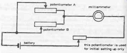
A very elementary form of analog computer is shown in Fig. 13-4, comprising two input potentiometers and an adjust potentiometer. The adjust potentiometer is used to set the meter reading to full scale deflection when both the input potentiometers are set to zero resistance. Movement of input potentiometer A will then produce a voltage drop in the circuit, shown by a reduction in the meter reading. This reduction will be proportional to the potentiometer movement. The same will happen if potentiometer B is adjusted. It is thus possible to calibrate the meter to indicate the position of either potentiometer A or potentiometer B setting.

Fig. 13-4. Elementary analog computer based on two potentiometers.
It follows that movement of potentiometer A (or B) can be "read" on the meter. If both potentiometers are set to mid -position, the adjust potentiometer can be used to set the meter needle in mid position. The scale can then be calibrated to read + values to one side-produced by moving either potentiometer to, say, the right, and-values to the other side-produced by moving either potentiometer to the left. Movement of either potentiometer will thus feed in a + or - signal, indicated by the meter. It follows that the circuit will, in fact, perform analog addition and subtraction of numerical values fed into it by movement of potentiometers A and B in appropriate directions and by calibrated amounts of movement.
The circuit also demonstrates one other major characteristic of an analog ' l' computer. The information it can accept, and gives in "read out," is $r infinitely variable. Its accuracy does, however, depend on the signal voltages introduced remaining exactly proportional to the quantities they represent. In practical analog computer circuits, feedback circuits are used to maintain this exact proportionality.
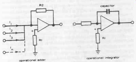
The basic component used in analog computers is an IC (normally represented by a triangular symbol). In the normal mode, it is an operational adder (summing amplifier), Fig. 13-5, adding the inputs (and taking account of their sign).
Factoring can be introduced by adding resistor R1, or direct multiplication or division by connection through a potential divider.
Other mathematical processes can also be performed by the op amp differentiation by replacing R1 with a capacitor, and integration by replacing R2 with a capacitor. The op amp is therefore a most versatile mathematical device, especially associated with other op amps and related circuits. It can also be connected in the inverted mode to change the mathematical sign of an input.

Fig. 13-5. Operational adder (left) and operational integrator (right).
The digital computer works in a much simpler way--and at first sight one which is much more limiting (although in fact this is not true). It works basically with bistable circuits which are either "on" or "off," and so all mathematical functions are performed in terms of binary numbers. Binary numbers are quite cumbersome when written out, e.g., 0 is 0 in binary notation
1 is 1
2 is 10 ("one oh," not ten)
3 is 11 ("one one," not eleven)
4 is 100
3 is 101
…. already the binary number is getting quite lengthy, and by the time it has reached 100, capacitor 100 is 1100100 in binary notation.
operational integrator
Not the sort of numbers to use for mental arithmetic, and when it comes to multiplication and division, multiplication is performed by repeated addition, and division by repeated subtraction.
But the system has one enormous advantage, as far as computer working is concerned. The "reading" of information is dependent only on whether a signal is present (on) or not (off). It does not depend on the strength of the signal at all, provided it is not weaker than a certain minimum necessary to trip the bistable circuit. Thus it should be-and is-a very much more precise system than an analog one.
The fact that it is apparently cumbersome does not matter at all for computers. The speed at which a bistable circuit can work is so fast that the actual number of individual binary digits, or "bits," which the computer has to process is largely immaterial. And all the operations can be performed by logic gates connected in logic circuits to cover exactly the functions required.
Another great advantage of digital circuits is that the basic information is simple on-off information which can readily be stored in a memory circuit, to be called back into the circuit at any point required. Storage can be done in magnetic cores (literally nothing more than tiny magnetic coils mounted at the crossing points on a grid of horizontal and vertical wires). A "bit" can be stored at any point in the memory, or recalled from the memory, by signaling that particular grid reference.
Magnetic core memories have the advantage of being cheap, compact and reliable. Once the stored information has been recalled, however, it lost from the memory (although some magnetic cores do have a facility to retain memory). For permanent storage, or where memory may be required in sequence, magnetic tape is used.
Today, solid-state memories are normally preferred to core memories, the main reason being that they are less expensive. Also they are, generally more reliable. Solid-state memories do have one basic disadvantage, though, they are volatile, meaning that if they lose power the memory content is also lost. This is typical of a RAM (random-access memory).
There are various ways in which this limitation can be overcome, such as preprogramming, or "burning-in," information which cannot be erased.
An example of this is the PROM (programmable read-only memory). Also, there are erasable PROMS, and reprogrammable ROMs.
Equally, for additional memory storage, a disk ("floppy disk") is often preferred to tape. The reason in this case is the quicker access to a given point in the memory. This can be located directly in the case of a disk. With a tape, the actual position required on the tape has to be found by forward/ backward search along the length of the tape.