AMAZON multi-meters discounts AMAZON oscilloscope discounts
The stock material for making printed circuit boards (PCBs) is copper-clad phenolic resin laminate (SRBP) or glass-fiber laminate. For general use these boards are single-sided (clad on one side only) and nominally 1.5mm thick (about 1/16 in.).
The procedure for making a PCB involves:
1. cutting the board to the required size and cleaning the copper surface.
2. making a drawing of the conductors required for the circuit on the copper in a resist ink.
3. etching away uncovered copper areas in a chemical bath.
4. removing the resist ink to expose the copper conducting areas or lands.
5. drilling the copper lands ready to take the component leads.
6. degreasing and cleaning the boards as necessary to ensure that the lands take solder readily.

Fig. 21-1. Horizontal mounting of components on a PC board takes up more space,
but is usually more convenient than vertical mounting (except for transistors).
PLANNING THE CIRCUIT DRAWING
Familiarity with the physical size of components to be accommodated on the board is essential, so that holes for leads, etc, can be correctly positioned. There are two ways in which resistors and capacitors can be mounted-horizontally or vertically (Fig. 21-1). Horizontal mounting is usual for resistors as this reduces lead length to a minimum.
Holes are then spaced a sufficient distance apart to allow for easy 90-degree finger-bends on the leads. The same consideration applied to tubular capacitors, mounted horizontally.

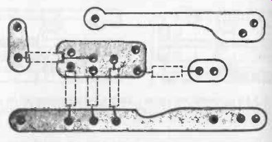
Fig. 21-2. If it is (or seems) impossible to avoid a crossing connection on
a PC board, stop the crossing lines short (left) and complete the connection
with a bridge of insulated wire soldered in place.
The physical size of capacitors, however, may be much larger than resistors, when vertical mounting may be preferred to save space.
Mounting holes then only need to be a little more than half the diameter of the capacitor, matching the position of the top lead taken down the side of the capacitor. Some capacitors have both leads emerging from the same end, especially for vertical mounting on a PCB. Spacing between holes, however, should not be less than twice the thickness of the board (i.e., 1/8 in.).
Transistors need reasonably wide spacing for their leads. Exceptions are transistor types with leads intended to plug directly into a PCB, and certain power transistors needing special mounts. In these cases, hole positioning follows the transistor lead geometry. Integrated circuits normally plug directly into matching IC sockets, the latter being mounted on the board in holes drilled to match the pin positions.
Layout starts with a tentative design of component positions, sketching in the connections required, (i.e., the areas of copper which will eventually form the conducting lands). No connections on a PCB can cross, and a certain amount of trial-and-error sketching is usually needed to achieve this requirement, altering component positions as necessary. If it seems impossible to achieve a complete circuit without crossing connections, then such points can be terminated on the PC drawing on each side of the crossing point, and subsequently completed during assembly of the circuit by bridging with a short length of insulated wire, just as a component normally acts as a bridge between adjacent conductors, Fig. 21-2.
FINAL DRAWING
Having arrived at a suitable layout, with connecting points for component leads indicated by blobs (.), a tracing can then be made of this PCB plan. Certain general rules apply in preparing the final drawing.
1. Conductors should not be less than 1/16 in. wide.
2. Conductors should be spaced at least 1 Beta 2 in. apart.
3. There should be at least 1 Beta 2 in. between a conductor and the edge of a panel.
4. Bends of junctions in conductors should be radiused or filleted, not sharp-edged.
5. Allow sufficient area of copper around a connecting point so that the copper width at this point is at least twice that of the hole size subsequently to be drilled through it, and preferably more. (Typical hole sizes for miniature resistors, capacitors and transistors are 1 Beta 2 in.).
These points are illustrated in Fig. 21-3, at least 1 Beta 2" In from odes of Panel round off al corners conductors at least 1/16" wide at least 1 Beta 2" clearance between conductors at least 1/16" width of copper around holes Fig. 21-3. Basic recommendations for planning conductor widths and spacings on PC boards.

Fig. 21-4. Quite large areas of copper can be left on low voltage battery
powered circuits. There is no need for consistent widths (or shapes) of conductors.
It is not necessary to draw all conductors neatly and uniform in thickness. Relatively large solid areas can be left to accommodate a number of common connecting points, simplifying the amount of drawing necessary, see Fig. 21-4. Large solid areas should, however, be avoided in any part of a circuit carrying high current as this could cause excessive heating of the copper, possibly making it delaminate as it expands. Thus, on a PCB for a mains -operated circuit, for example, the maximum area of any particular copper land should not be more than about 1 square inch.
The final drawing is transferred in reverse on to the copper (hence the use of tracing paper). This is because the circuit, as originally planned, shows the component side of the board, which is the plain side. Thus the true pattern for the copper side is reversed, mirror-image fashion. But before transferring the drawing to the board, the copper surface must be cleaned. This is done by washing with detergent and then drying.
A test for cleanliness is to hold the board copper-side up under a tap and let water run on to it. If the water flows freely over the whole area, it is free from grease. If dry patches appear on the copper, these areas are still greasy and require further cleaning.
After tracing the (reversed image) pattern on to the copper, this pattern is then painted in with resist ink or a resist marker pen (much easier to use than a brush and ink). Make sure that all the land areas are properly filled, but avoid applying too much ink as this could overrun the required outlines. Finally, allow to dry, which should take about 10 to 15 minutes.

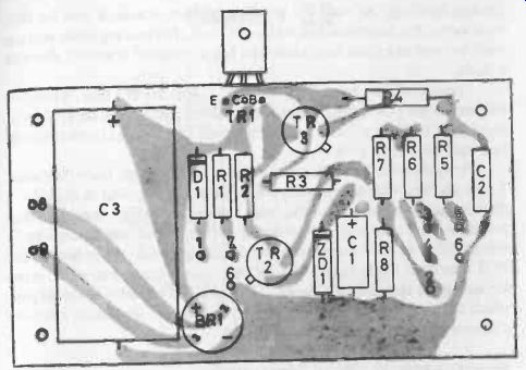
Fig. 21-5. Example of a printed circuit design with copper area shown shaded
and position of components indicated.
ETCHING
The board is then transferred to an etching bath. This can consist of a solution of ferric chloride, or proprietary printed circuit etching fluid poured into a shallow plastic tray. The board is placed in the bath copper side up and left until all traces of copper have disappeared from the surface.
Time taken for this will vary with the temperature of the solution and its strength. The process can be speeded up by "rocking" the bath gently or stirring with a soft brush.
After etching is completed the board is removed, washed under running water to remove any traces of chemical, and dried with a soft cloth.
The etching solution can be kept for re-use, if required.
To remove the resist ink, a further liquid known as etch-resist remover should be used. This can be brushed on to the board and then rubbed with a soft cloth, or applied to the cloth first and then rubbed over the board.
It should only take a minute or so to remove all the ink, leaving the copper patterns fully uncovered and clean. Wash and dry the board again at this stage to remove any residual traces of etch -resist remover.
Drilling comes next. The following rules are very important:
1. Always drill with the copper side uppermost, i.e., drill through the copper into the board.
2. Always use a sharp drill (preferably a new one).
3. Always use a backing of hard material under the board to prevent the point of the drill tearing a lump out of the back of the board when the point breaks through.
4. Spot the point to be drilled with a small center punch to prevent the drill running off its correct position when starting to drill.
Use of an electric drill in a vertical drill stand is best for drilling PCBs.
However, because of the small size of drill used, breakage rate of drills can be high if the work is pushed too hard.
The original tracing will now come in handy again for marking the component positions on the plain side of the board, as a guide for component assembly--Fig. 21-5. Components are always assembled on the plain side, with their leads pushed through their mounting holes until the component is lying flush with the board, Fig. 21-1. The exception is transistors, which should be mounted with their leads left fairly long (and preferably each lead insulated with a length of sleeving to prevent accidental shorting if the transistor is displaced).
MOUNTING AND SOLDERING
Before mounting components in position for soldering the copper side should be cleaned again. It will probably have picked up grease marks through handling. An ordinary domestic powder cleaner is best for this, used wet or dry, and rubbed on with a soft cloth. The running water test can again be used as a check for cleanliness, but if the board is wetted, dry with a cloth.
Components are normally soldered in place, one at a time, with their full lead length protruding. Excess length of wire is then cut off as close as possible to the solder. Some people, however, find it easier to cut the leads to length first, then solder.
Provided soldered joints are completed rapidly, in not more than about 3 seconds, heat-damage to either the board or a component is If the iron has to be held in contact with the lead for longer than this, then something is wrong with the soldering technique and heat damage could result, either to the component or by the lifting of the copper land on the PCB. The most likely causes of overheating are using an iron which is not hot enough or too small for the job; attempting to rework a soldered joint which has not taken properly; and trying to remove a lead which has been soldered into the wrong hole.
SIMPLIFIED PRINTED CIRCUIT CONSTRUCTION
As a supplement to drawing-and for making neater straight lines there are available rub -down transfer sheets of lines, bends, blobs for connecting points, etc., which can be used to build up the required pattern on the copper, supplemented with ink drawing where necessary. These transfer symbols are resistant to etching fluid, so serve the same function as drawn or painted lines, etc.
It is also possible to buy self-adhesive copper foil precut in the form of lines, bends, etc, similar to transfer strips, but which can be pressed down on to a plain panel to complete a printed circuit directly, without the need for any etching treatment. Further shapes can be cut from self-adhesive copper foil blanks. With PC boards made up in this fashion continuous (conductor) sections can be made up from overlapping pieces, provided positive connection is made by solder applied over the joint line.