3-1 A television receiver is a complex electronic mechanism.
Fifteen or more tubes are required to produce the picture and sound in very small television receivers, while as many as 35 to 40 tubes are used in larger, more expensive models. The reception of ultra-high frequency television signals is accomplished through the use of very critical circuits which require meticulous design and construction.
In a field as young as television, it is not unusual that manufacturers have found many different ways to solve the problems of video circuit design. Time and the all important proving ground in the customer's home will indicate the circuits and designs which perform the best. By familiarizing himself with all of the basic circuits commonly employed in television receivers, the .technician will be able to understand all of the various receivers. With an understanding of fundamentals, the reader will readily appreciate how combinations of the basic circuits may be grouped to make up the numerous commercial receivers now on the market.
Television receivers may be divided into three groups: (1)
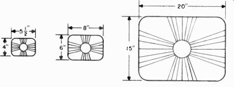
Figure 1. Relative picture sizes of seven inch, ten inch, and projection
television receivers.
Direct view receivers with electrostatic picture tubes, 7 inches or less in diameter; (2) Direct view receivers employing magnetic picture tubes ranging from 7 inches to 20 inches in diameter; (3) Projection receivers in which the image is thrown from the face of the picture tube onto a screen. Picture sizes as large as several square feet are obtained in this manner.
The relative picture sizes of receivers falling into each of these categories are shown in Figure 1. Many basic circuits are common to receivers in all three categories, but there are wide variations in those circuits which operate the different types of picture tubes and projection systems.
To simplify this discussion of the television receiver and make, it easier for the reader to understand, the receiver will be separated into six basic sections as shown in the block diagram of Figure 2.
1. The R-F Section
2. The Video Channel
3. The Sweep Circuits
4. The Power Supplies
5. The Picture Tube
6. The Sound Channel
All of the basic circuits used in each of the six sections of the receiver will be described in detail in this chapter. At the end of the chapter, combinations of these circuits will be grouped into complete receivers in each of the three categories previously mentioned.
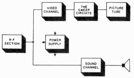
Figure 2. The six basic sections of the television receiver.
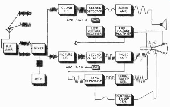
Figure 3. Block diagram of a television receiver with waveforms at input
and output of stages.
3-2 Block Diagram of a Typical Television Receiver. Before beginning the detailed description of the circuits used in tele vision receivers, it is well to summarize the operation of a typical complete unit. This may be accomplished by following a signal through the receiver. The path of the television signal through the receiver is traced with reference to the block diagram shown in Figure 3.
FREQUENCY IN MEGACYCLES
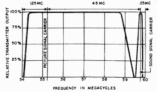
Figure 4. A typical television channel.
The antenna receives both the sound and picture signals, which are coupled to the receiver input by a suitable transmission line. Referring to the diagram of a typical channel as shown in Figure 4, it is apparent that the RF amplifier and mixer tuned circuits must have a bandwidth of 6 Mhz, if both the video and sound signals are to be passed.
Television receivers are of the superheterodyne type in which a local oscillator beats with the incoming signals in a mixer stage. Since there are two separate carriers in the RF and mixer circuits, the local oscillator, beating with each, will produce two IF signals in the plate of the mixer tube.
The plate of the mixer tube feeds filter networks which separate the video and sound IF signals, diverting them to the respective IF systems. After this point in the circuit, there are actually two independent receivers, either of which can operate without the other. One is an FM receiver which reproduces the sound, the other is a video receiver which forms the image on the picture tube.
The sound channel consists of IF amplifier stages, a limiter, a discriminator, and a conventional audio frequency amplifier.
The video channel begins with the intermediate frequency amplifiers which receive the video IF carrier from the mixer.
After passing through several IF stages, the video-modulated signal is delivered to a diode detector which acts as a demodulator in the conventional fashion. The detected signal passes through one or more stages of video amplification. The video amplifier response must be essentially flat from below 60 cycles to4 megacycles. The video signal is finally applied to the grid of the cathode ray tube and varies the intensity of the electron beam according to the shades of black and white in the picture.
At the output of the video amplifier there is a circuit which inserts a d-c component on the picture tube grid to reproduce the average brightness of the television picture.
Usually the video signal is tapped at the output of either the video detector or video amplifier and fed to a sync separator tube, which passes the sync pulses and clips off the video information. The sync pulses are then passed through an amplifier in whose plate circuit there are circuits which separate the horizontal and the vertical pulses. These pulses control the operating frequencies of horizontal and vertical sawtooth generators, in order to keep them in step with the transmitter.
Both sweep signals are then amplified and fed to the horizontal and vertical deflection plates (or coils). In this way, the beam in the picture tube is synchronized with that in the camera tube at the transmitter.
As the beam in the picture tube sweeps across the fluorescent screen, the signal on the grid of the tube produces the proper variations in the beam intensity and so reconstructs the television picture element by element and line by line.
The power supply requirements of the receiver are two-fold; First, a low voltage (300 to 400 volts) supply is required for the plates and screens off all the tubes, except the cathode ray tube; and second, a high voltage power supply is required for the picture tube. The high voltage required varies between 2,500 and 30,000 volts, depending upon the type and size of the picture tube.
THE R-F SECTION
3-3
The RF section of a television receiver must perform a number of functions: It must select the desired television signal consisting of sound and picture carriers; it must convert these signals to individual intermediate frequencies; and direct them to the audio and video channels. The RF section consists of the antenna input circuits, an RF amplifier (not used in all receivers), the local oscillator for superheterodyne operation, and the mixer. Since there are twelve television channels, extending from 54 to 216 Mhz, provision must be made, in the design of these circuits, for great frequency coverage. When tuned to any particular channel, the RF circuits must have a bandwidth of 4 to 6 Mhz, to pass the video and audio signals.
Wide band circuits operating at the high frequencies used for television bring about problems which are not encountered at standard broadcasting frequencies. The layout of the chassis and components, the inductance and capacity of leads, and the interelectrode capacities of tubes become important factors.
Miniature tubes have been developed which satisfy the requirements of these high frequency circuits.
Stray inductance and capacitance in the RF section of a television receiver is so critical that even a slight disturbance of lead or part positioning may cause a previously perfect receiver to become inoperative. In design and manufacture, all parts must be carefully positioned and leads must be kept as short and direct as possible.
Because excessive losses occur if ordinary insulating materials are used at high frequencies, special insulating materials are required in television receivers.
Frequency stability is an important factor in television receivers, because it is much more difficult to design stable equipment for high frequency operation than for use at regular broadcasting frequencies.
3-4 Tubes. Miniature tubes have low interelectrode capacitances and high mutual conductances (gm). Since the gain of an amplifier is proportional to mutual conductance, high mutual conductance miniature tubes simplify somewhat the problem of obtaining high gain amplifiers at television frequencies. Circuit capacity is important because it limits the size of the plate load resistor of the amplifier tuned circuits. The higher the capacity, the lower is the load resistor required for a broad band response characteristic. The gain of an amplifier is proportional to the size of its load resistance, so that it is desirable to make this resistor as large as possible by keeping the circuit capacity low.
In the design of broadcast receivers, pentodes have long been preferred to triodes because of their higher gain and stability.
In television receivers, the triode has again assumed importance because of several characteristics which make it superior to the pentode. The triode has fewer grids than a pentode and develops less noise. In highly sensitive television receivers, tube and circuit noise is about 10 microvolts. This is as great as some parts of the input signal. Tubes which generate the least amount of noise are therefore preferred. Triodes produce about one-third as much noise as a pentodes.
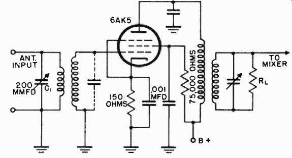
Figure 5. Pentode amplifier.
Another desirable characteristic of the new miniature triodes, designed for high frequency operation, is their reduced grid-to plate capacitance which makes them less likely to oscillate in amplifier stages. Their lower interelectrode capacitance reduces the degree of tuned circuit loading required in order to obtain a broad band response. Higher plate load resistance increases the amplifier gain of triodes.
Miniature tubes which are suited for broadband high frequency operation because of their low capacities and high mutual conductance are the 6AK5, 6AG5, and 7W7 pentodes, the 6J4, 6J6, and 7F8 triodes.
3-5 R-F Amplifiers. Not all television receivers employ RF amplifiers. In the primary operating areas of television stations, signals are strong enough so that an RF amplifier is not necessary.
There are several points in favor of the use of an RF stage.
Increased selectivity and reduced image response result when an RF amplifier is used. The added gain an RF amplifier produces, improves the signal-to-noise ratio of the entire receiver, because it minimizes the effects of the noise generated in the mixer tube. An RF amplifier isolates the oscillator from the antenna and prevents excessive radiation from the receiver, an important factor in crowded urban areas.
Several circuits and circuit variations are used in television RF stages.

Figure 6. Grounded-grid RF amplifier.
3-6 Pentode R-F Amplifier. A pentode RF amplifier is illustrated in Figure 5. The 6AK5 and 7W7, high mutual conductance pentodes, are suitable for broadband, high frequency operation in such a circuit. A double-tuned, over-coupled transformer is used between the grid of the RF amplifier and the antenna. Its primary is tuned by capacitor C-1 to provide a resonant circuit at the desired frequency. In the plate circuit, another parallel tuned circuit is used, loaded by resistor R-1, to obtain a response characteristic 6 Mhz wide. The RF signal appearing across this resonant circuit is coupled directly to the grid of the mixer stage.
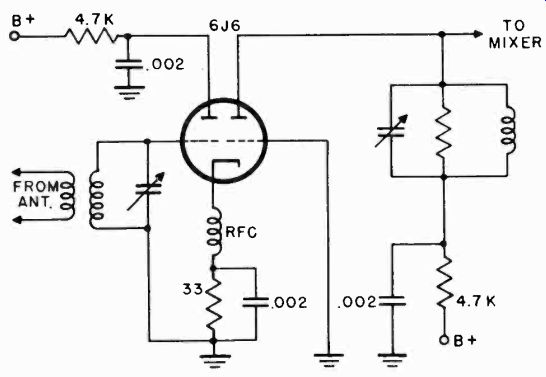
Figure 7. Cathode-coupled RF amplifier.
3-7 Grounded-Grid Amplifier. In conventional RF amplifier circuits, a triode would oscillate if used at television frequencies because of its high interelectrode capacity. The grounded-grid RF amplifier shown in Figure 6 was designed to eliminate this oscillation without the use of neutralization. The grid of the tube is grounded and acts as a shield between the input and output circuits, thus preventing the tube from oscillating. The input signal is injected into the cathode. The varying RF signal produces a fluctuating potential difference between the grounded grid and the cathode, causing changes in plate current. The grounded-grid amplifier, using triodes such as the 6J6 or 6J4, is simpler in construction than a pentode amplifier and requires fewer components.
3-8 Cathode-Coupled R-F Amplifier. Figure 7 shows a dual triode used as a cathode-coupled amplifier. This circuit is in reality a combination of two amplifiers. The first triode section is used in a cathode-follower circuit with the input signal fed to its grid. Normally, the output of a cathode-follower is taken from the cathode of the tube. The tube shown has a common cathode for both triode sections, and therefore, the output signal of the cathode-follower is connected to the cathode of the second section. The second triode is a grounded grid amplifier, and since in such a circuit the cathode is the input, interstage coupling is complete within the tube.
The addition of the cathode follower stage before the grounded grid amplifier has several advantages. The input of the cathode follower has low capacity and broad bandwidth. The additional stage isolates the antenna from the local oscillator better than does a single RF stage. Oscillator radiation to nearby receivers is therefore negligible. The overall gain of this RF amplifier is about the same as that of a single pentode. If a dual triode, having separate cathodes, were used, the cathodes would have to be connected together.
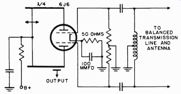
Figure 8. Push-pull RF amplifier.
3-9 Push-Pull R-F Amplifier. Push-pull RF amplifiers are found in some receivers. These circuits possess excellent stability at high frequencies. Atypical circuit is shown in Figure 8. The input signal is fed from the antenna through a balanced transmission line to the grids of a dual triode. The plate tank circuit consists of a quarter wave section of balanced transmission line. This quarter wave section is equivalent to a high Q parallel-tuned circuit. The transmission line can be tuned over a band of frequencies by moving a shorting bar along the parallel conductors. The push-pull amplifier has high gain, low capacity, and is stable in operation by virtue of its symmetry.
3-10 The High Frequency Oscillator. The purpose of the local oscillator in a television receiver is identical to that of the oscillator in a conventional superheterodyne. The oscillator signal beats with the incoming television signal to produce the picture and sound IF signals.
An important problem in the design of television receivers is that of oscillator stability. Excessive oscillator drift results in corresponding intermediate frequency drift and deterioration of the video and audio response. In extreme cases, the oscillator frequency may shift far enough so that the audio carrier output of the mixer stage is moved out of the pass band for which the sound IF amplifier is tuned.
Temperature change and supply voltage variations are the major causes of oscillator drift. Most materials have a positive temperature expansion coefficient; that is, with a rise in temperature, they expand. As a result, an increase in temperature causes an increase of inductance and capacitance in the oscillator circuit, and a corresponding decrease in frequency.
Since ceramic materials have a practically zero temperature coefficient, band switches and sockets are usually made of these materials.
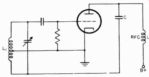
Figure 9. Shunt-fed Hartley oscillator.
To overcome the effects of capacitance which increases with temperature, a small capacitor with a negative temperature coefficient is often added across an oscillator coil. Inductance increases may be minimized by the use of suitable types of wire, such as Invar and Nilvar, which have negligible linear expansion coefficients. It is interesting to note that while receiving circuits use high L to C ratios for best efficiency, a low L to C ratio is preferred in oscillators. If the capacitance is made relatively large, it tends to minimize the effects of capacitance changes due to tube warm-up and plate voltage variations.
In order to reduce oscillator "pulling" to a satisfactory point, it is necessary to use separate tubes for the oscillator and mixer stages of a television receiver. Pulling is the tendency of the oscillator to lock in or approach the frequency of a signal near its own frequency (in this case, the incoming RF signal). The fact that the comparatively high interelectrode capacities of multi-grid converter tubes makes them undesirable at high frequencies, is another reason why separate mixer and oscillator tubes are found in television receivers.
Several types of oscillator circuits are found in television receivers. At present, the Hartley, the Colpitts, and the Ultraudion are the most popular.
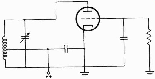
Figure 10. Series-fed Hartley oscillator.
3-11 The Hartley Oscillator. The Hartley is one of the simplest self-excited oscillators. Its distinguishing feature is the tapped coil, L-1, used to obtain the feedback necessary for oscillation. A shunt fed circuit is shown in Figure 9. The coil is connected between the plate and the grid. The tap, usually located nearer the grid end, is connected either directly or through a condenser, to the cathode of the oscillator tube. A blocking condenser, C, is used to isolate the high positive d-c voltage on the plate from the negative d-c voltage on the grid. The RF grid current flows in the lower section of the coil, while the RF plate current flows in the upper section of the coil. The phasing of the plate and grid currents in the coil is such that positive feedback to the grid is obtained and oscillation takes place.
Both shunt (Figure 9) and series (Figure 10) feed are illustrated to demonstrate the detailed circuit modifications necessary to change from one method of feed to the other. Shunt feed is well adapted to applications in which it is desirable to keep the tuned circuit at ground potential. This is accomplished only at the expense of using a well designed RF choke in the B plus lead. Series feed eliminates the need for this choke but requires that the tuned circuit be at a high d-c potential (plate voltage) above ground.
The Hartley oscillator does not depend on the grid-plate capacity of the oscillator tube for feedback and will, therefore, work well with almost any type of triode, tetrode, or pentode.
By modifying the basic circuit as shown in Figure 11, the Hartley can be made to cover several widely separated frequencies.
In position 1 of the switch, L-5 is in the circuit in combination with capacitor C-1. Other frequencies are obtained by placing inductances L-1, L-2, L-3, or L-4 in parallel with C-1, which is always in the circuit. The number of switch points is determined by the number of television channels which the receiver must cover. The variable capacitor, C-2, is placed in the circuit for fine tuning and to adjust for frequency drift.
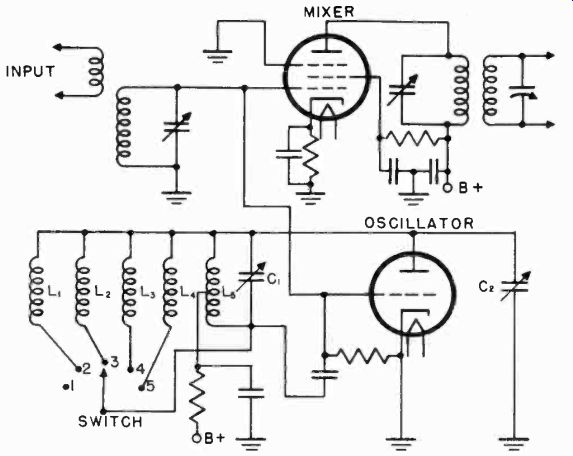
Figure 11. Hartley oscillator for covering widely separated frequencies.
3-12 Colpitts Oscillator. The Colpitts oscillator obtains the feedback necessary to support oscillation by dividing the tuned circuit into two parts, as shown in Figure 12. This division is accomplished by means of a capacitive voltage divider made up of C-1 and C-2 in series, shunted across L. It will be noticed that the principle involved is the same as that used in the Hartley circuit, except that it is the capacitor which is tapped instead of the coil. The RF voltage across C-1 is the plate portion, and the RF voltage across C-2 is the grid portion. The feedback ratio is therefore dependent on the ratio of the two capacitors.
The smaller capacitor has the larger RF voltage across it, since its reactance is greater. Because the ratio of the reactance does not change with frequency, a constant feedback ratio over a wide tuning range can be maintained, providing the reactance ratio is not disturbed. The ratio can be kept constant by adding a separate variable condenser, or by making C-1 and C-2 parts of a split stator condenser.
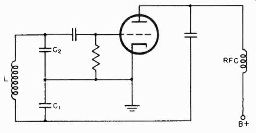
Figure 12. Colpitts oscillator.
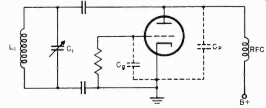
Figure 13. Ultraudion oscillator.
3-13 Ultraudion Oscillator. The Ultraudion oscillator (Figure 13) has the distinguishing characteristic that there is no visible division between the grid and plate portions of the coil L-1. This circuit has no coil tap as does the Hartley, or capacity divider as does the Colpitts.
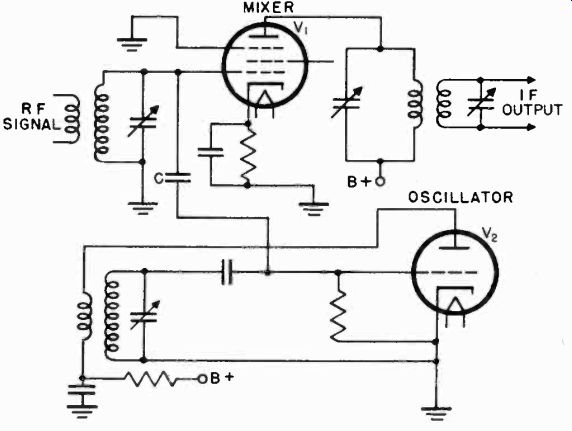
Figure 14. Capacitive-coupled mixer oscillator.
In the Ultraudion, the grid-to-cathode capacitance Cg and the cathode-to-plate capacitance Cp form a voltage divider which performs the same function as do the dividing capacitors used in the Colpitts circuit. In other words, the operation is exactly the same as the Colpitts circuit, except that the dividing capacitances are the interelectrode capacitances of the tube plus stray capacitance in the wiring. This makes the feedback ratio entirely dependent upon the characteristics of the tube, and the stability subject to the heating effects on the tube elements.
Adjustment of feedback is possible by the addition of a condenser between the grid and cathode, or plate and cathode, or both.
The advantage of the Ultraudion circuit is that it is simple and requires comparatively few components, since it uses inter electrode capacitances in place of external components.
3-14 The Mixer. In the superheterodyne television receiver, the mixer's function is the combining of the incoming RF carrier with the receiver's oscillator signal to produce a lower frequency (intermediate frequency). In order to produce this intermediate frequency, the mixer must operate as a non-linear device on the curved portion of the plate characteristic of the mixer tube. In ordinary broadcast receivers, a single tube, known as a pentagrid converter, often performs the functions of the oscillator and mixer. At television frequencies, the stability of the oscillator section In a penta grid converter is very poor. To avoid excessive frequency drift, separate tubes are used for the oscillator and mixer stages in current television receivers.
A typical mixer circuit is shown in Figure 14. Here both the RF signal and the local-oscillator voltage are applied to the control grid of a pentode, V-1. Instead of capacitive coupling to the oscillator through C, inductive coupling may be used. A circuit using inductive coupling is shown in Figure 15. The use of two tubes in the circuit arrangements of Figures 14 and 15 results in stable oscillator performance and maximum gain, by permitting the use of a high transconductance mixer tube.
The greater the conversion efficiency of the mixer stage, the better is the signal-to-noise ratio of the circuit. That is, for a small signal input, more IF voltage is produced at the plate, which in turn helps to overcome the mixer conversion noise.
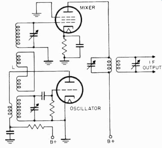
Figure 15. Inductively-coupled mixer-oscillator.
Only the beat frequency of the RF signal and the oscillator is to be passed on to the IF stages; hence, the plate tank circuit of the mixer tube is tuned to this intermediate frequency. The RF and oscillator frequencies in the plate circuit are by-passed to ground.
3-15 Dual Triode Mixer-Oscillator Circuits. A dual triode, such as a 6J6 or 7F8 is often used as a mixer and oscillator.
The incoming signal is applied to the mixer grid and the oscillator voltage is injected into the grid or cathode.
In Figure 16, one section of a 7F8 dual triode is connected as a Hartley oscillator. The cathode of this section is capacitively coupled to the cathode of the mixer stage. The intermediate frequency appears in the plate circuit of the mixer triode. In Figure 17, the oscillator voltage is injected into the grid.
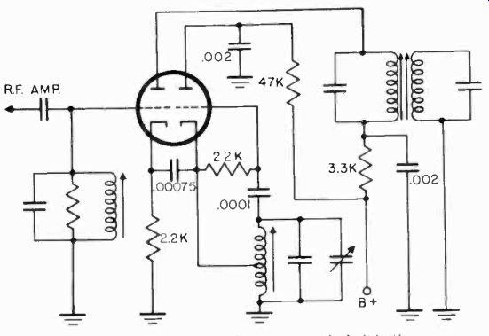
Figure 16. Mixer-oscillator using cathode injection.
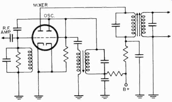
Figure 17. Dual triode mixer-oscillator using grid injection.
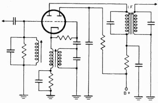
Figure 18. Mixer-oscillator using dual triode with common cathode.
A 6J6 which has a single cathode common to both triode sections may also be used as a dual mixer-oscillator tube if it is connected as shown in Figure 18. The RF input signal is injected into the grid of the first section. This sets up a varying voltage across the inductance in the cathode circuit. The second triode is operated as a modified Colpitts oscillator with its grid coil coupled to the inductance in the cathode. Cathode-coupled mixing thus takes place and produces an intermediate frequency in the plate circuit of the mixer section.
Dual triode mixer-oscillator circuits do not exhibit the disadvantages of single tube mixer-oscillator circuits which were previously mentioned, because there is sufficient isolation between sections of the tubes used to eliminate these effects.
3-16 Separation of Video and Audio I-F Frequencies. In addition to the video IF frequency signal in the mixer of a television receiver, there is also generated an audio IF carrier and its associated sidebands. The video IF frequencies of present receivers range from 25.75 Mhz to 26.4 Mhz, while the audio IF carrier may be from 21.25 Mhz to 21.9 Mhz. In most receivers, the video and audio IF signals are separated in the mixer stage, and fed to separate amplifiers.
Several methods are employed to separate the signals, all embodying much the same principle. Tuned circuits are placed in the mixer stage. Each circuit is resonated for the desired frequency which is then passed on to the proper IF amplifier. In Figure 19, a parallel combination consisting of a coil, L-1, and a capacitor, C-1, is placed in the mixer plate circuit and broadly tuned to pass the 4 Mhz video signal. The video signal is then fed to the video IF amplifier. A separate parallel circuit, L2-C2, is tuned to 21.9 Mhz, thus developing a maximum voltage at the audio frequency, but very little video signal voltage. The 21.9 Mhz sound carrier and its 25 khz sidebands are fed to the audio IF amplifiers.
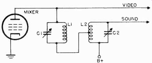
Figure 19. Circuit used to separate the video and audio signals.
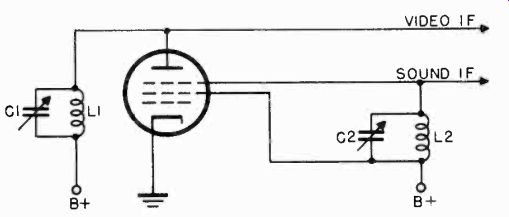
Figure 20. Plate and suppressor-screen tuned circuits for separating video
and audio signals.
In Figure 20, two parallel tuned circuits are again used, but in this case, the resonant circuit (L1-C1) for the picture signal is in the plate circuit, while the tuned circuit (L2-C2) for the sound signal is in the suppressor-screen circuit. Still another method uses a series parallel combination as shown in Figure 21. The video signals are developed across the parallel tuned elements (L1-C1) in the plate circuit, while the sound is taken from the capacitor in the series circuit formed by the inductance, L-2, and the capacitance, C-2.
Perfect separation of audio and video signals is not achieved by the above methods, and additional filtering must be employed in the respective IF amplifiers. Little trouble is encountered with video signals in the audio stages, since spurious amplitude modulation of the FM sound by the picture signals is suppressed in the limiter stages. On the other hand, sound signals can materially affect the picture quality if they are not properly filtered.
Rejection of sound signals which reach the video channel is obtained through the use of wave traps which are discussed later in this section.
3-17 Wide Band Tuned Circuits. The amplifier stages in the Figure. Series and parallel circuits tor separating video and audio signals.
RF and IF sections of a television receiver are coupled together by tuned circuits consisting of combinations of inductors, capacitors, and resistors. These tuned circuits must be designed and adjusted for a uniform 6 Mhz pass band in the RF circuits and4 Mhz pass band in the video IF circuits. At the same time, the shape of the response curve of the tuned circuits must be such as to attenuate the frequencies generated by stations operating on adjacent channels.
A simple tuned circuit consisting of a coil and capacitor connected in parallel is shown in Figure 22. This circuit has a characteristic such that when a voltage is applied to it at its resonant frequency, the impedance of the parallel combination is maximum. As the applied voltage is varied in frequency above and below the resonant point, the impedance of the circuit decreases as shown in Figure 23. Several curves are shown in the figure, each curve representing a different value of Q. Q is the ratio of a coils inductive reactance to its resistance. The significance of this ratio is indicated by the shape of the curves in Figure 23. The higher the Q, the sharper is the tuning of the circuit, and the greater is its selectivity. Another important factor is the fact that the higher the Q of a circuit, the higher the voltage developed across it. Thus, Q is a measure of the gain of an amplifier stage which uses tuned circuits.
The simple circuit of Figure 22 is inadequate for coupling television amplifier stages, because it discriminates against frequencies above and below its resonant frequency. In order to obtain a wideband frequency characteristic for RF, mixer, and IF stages, a transformer combination is employed as shown in Figure 24.
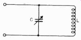
Figure 22. A parallel resonant circuit.
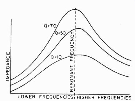
Figure 23. The effect of Q on the selectivity of a parallel tuned circuit.
Several resonant curves can result from this circuit, depending upon the degree of coupling between the primary and the secondary (the coefficient of coupling, is a measure of the amount of magnetic flux linking the primary and the secondary). In Figure 25, three conditions of coupling are shown. A loosely coupled circuit gives the resonant frequency characteristic of the simple tuned circuit. As the coupling is increased, a point is reached where the impedance of the circuit rises to a maximum. This degree of coupling is referred to as "critical coupling". At degrees of coupling greater than critical coupling, the impedance no longer rises, but the curve begins to broaden, resulting in the double humped characteristic of an overcoupled circuit.

Figure 24. A resonant and coupled coil.
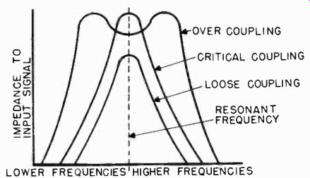
Figure 25. The effect of coupling on the response of a tuned circuit.

Figure 26. Transformer shunted with resistors to flatten and broaden its
response.
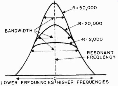
Figure 27. The effect of various values of load resistance on bandwidth of
coupling transformers.
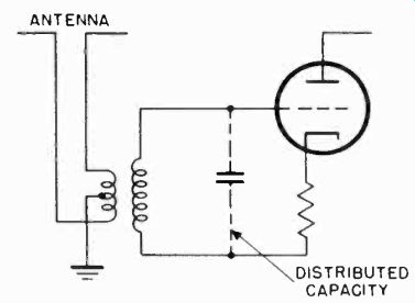
Figure 28. Antenna coupling circuit using untuned primary and tuned secondary.
The overcoupled circuit approaches the desired response for wideband television amplifiers. However, the dip at the resonant frequency is undesirable. This dip is minimized by shunting the primary and the secondary with low resistances as shown in Figure 26. This lowers the Q of the circuit and consequently its gain, but flattens and broadens the curve to secure the 6 Mhz bandwidth required. Figure 27 shows several response curves for different values of loading resistance. Special high gain tubes, such as the 6AC7, 6AK5, 6AU6, and 6J6, have been developed for television to compensate for the reduction in gain resulting from broad band coupling. Gains of approximately 10 to 20 are realized when these tubes are used in broadband circuits.
3-18 Antenna Coupling Circuits. A tuned wideband circuit is A required in the antenna input system in order to match the impedance of the antenna transmission line to the first amplifier tube. Two types of coupling circuits are illustrated in Figures 28 and 29. Figure 28 shows an untuned primary and tuned secondary transformer which permits impedance matching through adjustment of the number of turns in each winding. The secondary winding, and its distributed capacitance, form a resonant circuit. The tuned primary and secondary circuits of Figure 29 give double the signal gain of an untuned primary, tuned secondary circuit, having the same bandwidth. Impedance match is provided for through adjustment in the number of turns and the size of the shunting capacitance.
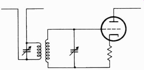
Figure 29. Antenna coupling circuit using tuned primary and secondary.
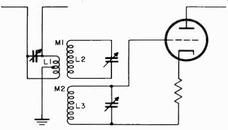
Figure 30. Double tuned antenna coupling circuit with tuned link added.
A third type of coupling is shown in Figure 30. A tuned link, L-2, is added to the double tuned circuit of Figure 29 and results in greater signal gain and selectivity.
The generation of the sound and picture intermediate frequencies in the mixer stage completes the functions of the RF section. From this point, the television receiver actually becomes a separate FM sound receiver and a separate video receiver with common power supplies. The sound IF signal is directed to distinctly separate audio circuits. The picture signals are fed to the video and sweep circuits which control the operation of the picture tube.
THE VIDEO CHANNEL

Figure 31. Block diagram of the video channel.
3-19 The video channel consists of the video IF amplifiers, the video second detector, the video amplifier, an automatic gain control circuit, and a circuit referred to as the d-c restorer.
These stages are arranged as shown in the block diagram of Figure 31. The video channel amplifies the video IF signals, detects them, and brings them up to a level at which they can properly modulate the grid of the picture tube.
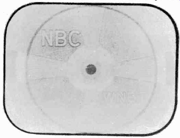
Figure 32. Test pattern showing effects of weak signal.
The sensitivity, selectivity, and bandwidth of a television receiver, with respect to video signals, is governed mainly by the characteristics of its video IF amplifiers. Only careful design and construction will bring about the required characteristics.
3-20 Sensitivity. The sensitivity of a television receiver may be defined as the minimum input voltage which will drive the grid of the picture tube from full brightness to cutoff when the receiver is operating at maximum gain. The amplitude of the video signal required at the picture tube to fully modulate the grid in this manner depends upon the design characteristics of the electron gun structure. Although the signal amplitude required varies with different picture tubes, 50 volts may be taken as an average. The gain of the RF amplifier, the video IF amplifiers, and the video amplifier must provide sufficient amplification to increase the level of the received signal to the required 50-volts. When the amplification of a receiver is increased, the signal required to provide the necessary 50 volts is reduced.
A receiver capable of great amplification can therefore produce satisfactory pictures with very weak input signals. There is, however, a limit to the amount of usable amplification. The amount of usable amplification is governed by the prevailing man made and atmospheric noise. When the noise signals are almost as strong as the television signal, a "washed-out", grainy picture is obtained. Noise streaks appear in the picture and synchronization is unstable. Figure 32 is a test pattern showing the effects of a weak signal. The minimum signal from which a satisfactory picture can be reproduced must of necessity be stronger than the prevailing noise.
3-21 Signal to Noise Ratio. The relation between a received signal and the prevailing noise is usually expressed as a ratio, referred to as the signal to noise ratio. In strong signal areas, the signal-to-noise ratio may be as high as 50 or more. The primary operating area of a television station is considered to include all locations where a video signal of more than 500 microvolts maybe received. Since the average noise level is normally about 100 microvolts, signal to noise ratios as low as 5 are commonly encountered.
As previously pointed out, the weakest television signal which will produce a usable picture is slightly greater than the noise level. In areas having a noise level of 100 microvolts, a signal of over 100 microvolts is necessary. Such a signal would therefore have a signal to noise ratio of more than one. If the gain of the receiver is sufficient to amplify weaker signals, say 50 microvolts, to a level of 50 volts at the picture tube, so much noise would be amplified along with the desired signals that the picture would be unpleasant to view.
With this understanding of minimum input signal level and the voltage required at the picture tube, it is possible to determine the gain needed in each amplifier stage of the television receiver. To amplify a 100 microvolt signal to a level of 50 volts, the overall amplifier gain must be 500,000 (50 volts divided by 100 microvolts). This gain might be derived in a television receiver in the following manner:
1. An RF amplifier with gain of 10.
2. I-F amplifier stages with gains between 8 and 15.
3. A video amplifier with a gain between 25 and 50. If it is assumed that the receiver has three IF stages, that the RF amplifier and each IF amplifier have a gain of 10, and that the video amplifier has a gain of 50, the following amplified voltages will appear at the specified points in the receiver for an input signal of 100 microvolts:
1. At the output of the RF amplifier-1,000 microvolts.
2. At the output of the 1st video IF amplifier--10,000 micro volts.
3. At the output of the 2nd video IF amplifier--100,000 microvolts.
4. At the output of the 3rd video IF amplifier--1,000,000 microvolts, or 1 volt.
5. At the output of the video amplifier (or the input to the grid of the picture tube) 50 volts.
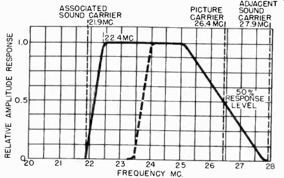
Figure 33. The ideal response curve for a television receiver.
Most television receivers now on the market have a gain of about 500,000 and, therefore, have a sensitivity of about 100 microvolts. Some of these receivers may not have an RF amplifier stage, in which case an extra video IF amplifier or video amplifier may be used to achieve this sensitivity. A few receivers have sensitivities as low as 1,000 microvolts, which means that they must operate in areas where strong signals exist.
3-22 Bandwidth. Closely associated with the sensitivity of a receiver is the bandwidth of its amplifiers. As the bandwidth of an amplifier is increased, its gain is decreased. The optimum bandwidth for passing the video signal is 4 Mhz. To achieve this wideband response at high gain is a very difficult problem. Circuit capacities, tubes, and components must be critically selected. Only high quality receivers have this wideband response and a maximum sensitivity of 100 microvolts. In less expensive receivers which employ small picture tubes, the bandwidth is purposely limited to a value not greater than 3 Mhz and often less than 2.5 Mhz. This means that the gain of each amplifier stage may be increased, and fewer stages used. There is little advantage in using 4 Mhz amplifiers with small picture tubes, because the spot size of the electron beam prevents the reproduction of any more detail than contained in a 2.5-3 Mhz signal.
With large tubes (10 inches or more in diameter) full use may be made of bandwidths of 3.5 to 4 Mhz.
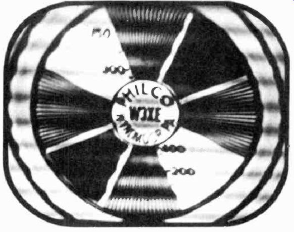
Figure 34. Test pattern showing effects of sound in the picture channel.
3-23 Selectivity. The selectivity of a television receiver reflects in its ability to differentiate between the desired video signal and signals of other frequencies. Selectivity is usually expressed in the form of a curve of output voltage plotted against frequency. The shape of the selectivity curve is chiefly determined by the response of the video IF amplifiers. The ideal selectivity curve for a television receiver, as shown in Figure 33, is therefore the same as the video IF response curve. Several important characteristics of the idealized curve should be noted:
1. The response falls to zero at 21.9 Mhz. This is the sound carrier intermediate frequency of the associated television channel. The associated channel sound signals must be greatly attenuated so that they will not pass through the video channel.
Should sound signals get into the picture, they will cause annoying band patterns in the picture, as shown in Figure 34. An attenuation of 40 db (a voltage ratio of 100 to 1) will fully reject the associated channel sound carrier.
Figure 35. The relationship between the response of a television receiver, the television signal, and signals in adjacent channels.
2. The video signal is uniformly amplified from 22.4 Mhz to about 25 Mhz. From this point, the slope of the curve falls gradually. At 26.4 Mhz, the relative amplitude response is 50%. The bandwidth of the video channel is considered to extend from 22.4 Mhz to the point on the response curve where the response has dropped to 50%. The frequency difference between 22.4 Mhz and 26.4 Mhz is 4 Mhz. In other words, the selectivity curve of an ideal television receiver is not flat over its entire 4 Mhz bandwidth. The response of the amplifiers is made to slope in this manner because it has been found that an amplifier with this characteristic passes the high frequency components of the television signal with less distortion than an amplifier whose response is flat to 4 Mhz and then drops off very suddenly. The dotted portion of the curve represents the response characteristic of a video IF amplifier, such as used in television receivers with small picture tubes. The pass band of the amplifier extends from about 23.9 Mhz to 26.4 Mhz, or 2.5 Mhz.
3. The response at 27.9 Mhz is zero. This is the sound carrier intermediate frequency of the higher adjacent television channel (Figure 35). Since this signal is very close to the picture carrier, it must be more sharply attenuated than the sound carrier at 21.9 Mhz. An attenuation of 60 db (a voltage ratio of 1,000 to 1) is recommended design practice.
The response characteristic of actual amplifiers does not normally resemble the ideal selectivity curve shown in Figure 33. To obtain this selectivity, sound traps are placed in the video IF amplifier stages. These traps attenuate the sound carriers on either side of the picture carrier and are responsible for shaping the response curve.
3-24 Intermediate Frequencies. Most manufacturers operate the receiver local oscillator at a higher frequency than the received signal, so that the video intermediate frequency signal appears on the low frequency side of the sound intermediate frequency signal, as shown in Figure 36. The intermediate frequencies indicated in this figure are 21.25 Mhz for the sound, and 25.75 Mhz for the video. These are the frequencies employed in RCA receivers. Other manufacturers sometimes use other intermediate frequencies. For example, Philco receivers are designed for a sound intermediate frequency of 22.1 Mhz and video intermediate frequency of 26.6 Mhz. G.E. and DuMont employ
21.9 sound and 26.4 video intermediate frequencies.
3-25 Video I-F Amplifier Circuits. To achieve the wideband response required in the video IF amplifiers, a number of methods are employed. One method utilizes overcoupled band pass amplifiers and another stagger tuned amplifiers. A third type of video IF amplifier system, now in use in some television receivers, is known as the intercarrier sound system or the dome system. Using this system, both the video and audio IF carriers are amplified together, eliminating the need for a separate sound IF system.
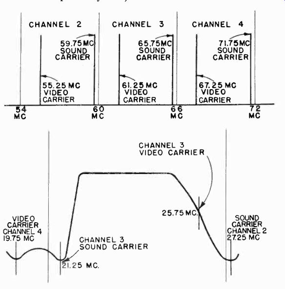
Figure 36. Video and sound RF frequencies, and video and sound IF frequencies.
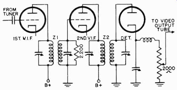
Figure 37. Simplified schematic of broadband overcoupled f-f amplifier.
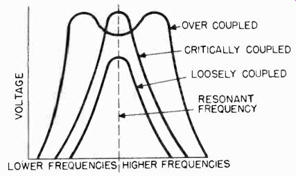
Figure 38. Effect of coupling on the response of a tuned circuit.
3-26 Overcoupled Circuits. A typical broadband, overcoupled video IF amplifier is shown in Figure 37. Except for the fact that its band pass is 4 Mhz, this IF amplifier is identical to the RF amplifiers previously described. The response characteristic of the over-coupled IF transformers Z-1 and Z-2 is shown in Figure 38. This response is shown compared to that of a loosely coupled and a critically coupled transformer. With loose coupling, the response is maximum over a narrow band of frequencies. If the transformer is critically coupled, the gain of the tuned circuit is increased, but is maximum for a narrow band of frequencies only. Finally, if the transformer is over coupled, the response curve broadens to include a wide band of frequencies.
In a broadband amplifier chain, each stage is not necessarily tuned to its full bandwidth. Slight compensating effects are made in each tuned circuit to produce a good overall characteristic. The IF response curves of a broadband amplifier chain designed in this manner are shown in Figure 39. The combination of the four curves produces a response which is substantially flat from about 22.5 Mhz to 25 Mhz.
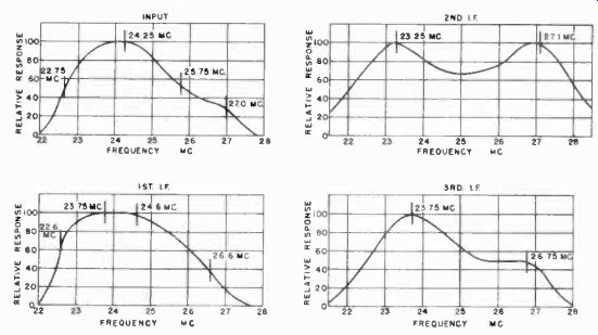
Figure 39. Response curves of the transformers of a broadband amplifier chain.
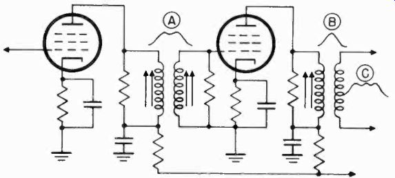
Figure 40. Simplified schematic and response curves of peaked and overcoupled
IF amplifier.
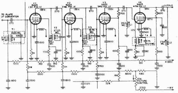
Figure 41. Stagger tuned i-f amplifier channel.
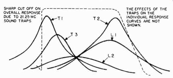
Figure 42. Response curves of stagger tuned IF amplifier.
A combination of over-coupled and peaked resonant circuits
is used in some receivers to obtain a wide response characteristic. By peaking one stage (B), the dip in the over-coupled stage (A) is minimized, as shown in Figure 40. The resultant response is that of curve C. 3-27 Stagger-Tuned Circuits. In a stagger-tuned IF system, each stage is peaked to a different frequency, and the overall response curve is the result of the combination of peaked stages.
In the circuit of Figure 41, four stages of IF amplification are employed to obtain the necessary wideband frequency response characteristic and adequate gain. The converter plate transformer, T-1, and each successive IF transformer have one tuned circuit each, and each is tuned to a different frequency.
The effective Q of each coil is fixed by the shunt plate load or grid resistor, so that the response of all of the stages together produces the desired overall curve. Figure 42 shows the response curves of each stage and the shape of the curve which results from their combination.
In order to obtain this band pass characteristic, the picture IF transformers are tuned as follows:
Converter transformer
First transformer
Second IF transformer
Third IF coil
Fourth IF coil
21.8 Mhz. (T-1 primary)
25.3 Mhz. (T-2 primary)
22.3 Mhz. (T-3 primary)
25.2 Mhz. (L-1)
23.4 Mhz. (L-2)
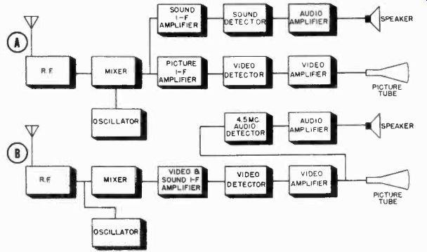
Figure 43. Block diagrams of receivers using conventional and intercarrier
sound systems.
In such a stagger tuned system, the correct overall response curve can not always be obtained by tuning the coils to specified frequencies. This results when the values of the components of a tuned circuit are slightly off and change the shape of the response curve of a tuned circuit. By shifting the frequency to which each circuit is tuned, compensation can usually be made for the off value components and the desired response obtained.
The response of the IF stages of a receiver changes slightly when the picture control is varied due to the Miller effect. This effect results in a change in tube input capacitance as the tube's gain is varied by grid bias changes. The change of input capacitance causes a slight detuning of the preceding IF coil and a slight change in response. The change is slight, however, and if the receiver is aligned at the correct grid bias, no difficulties are encountered in stagger tuned systems.
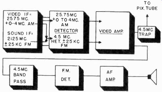
Figure 44. Operation of the intercarrier sound system.
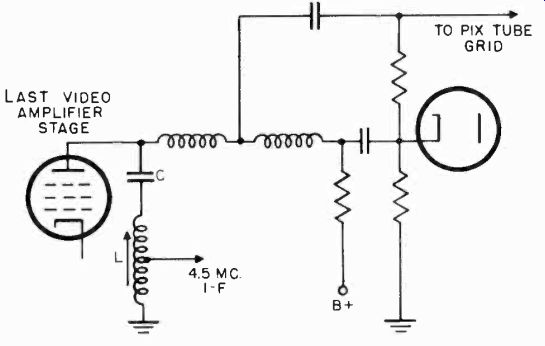
Figure 45. Circuit used to separate the sound carrier from the video signal
in intercarrier receiver.
3-28 The Intercarrier Sound System. The use of the inter carrier sound system eliminates the need for separate video and audio IF circuits. This system is in use in a number of receivers and considerably lowers component costs. The intercarrier sound system may be illustrated by comparing the block diagram of a conventional television receiver with that of a receiver using the intercarrier system, as shown in Figure 43. In the conventional receiver, (A), the individual picture and sound carriers are heterodyned in the mixer with the high frequency local oscillator to produce two separate IF carriers with their associated sidebands. The video carrier is fed to the video IF amplifier, and then to the video detector. It is further amplified by the video amplifier, and finally impressed upon the grid of the picture tube. Similarly, the FM sound carrier is fed to the sound IF amplifier, detected, and further amplified to a level sufficient to drive the speaker. Note that two separate IF amplifying systems are required in such a television receiver circuit.
The operation of the intercarrier sound system is explained with reference to Figure 44.
1. The incoming television signal is heterodyned to produce sound and video IF carriers.
2. The combined sound and video IF carriers are amplified by the same IF amplifying system.
3. The video signal is detected and amplified as usual. It is then fed to the picture tube.
4. The audio signal, separated from the video signal at the video amplifier output, has already been amplified in both the picture IF channel and the video stages.
5. The 4.5 Mhz FM carrier is fed to an FM detector and audio amplifier.
A simple circuit for separating the sound carrier from the video signal is shown in Figure 45. Since the audio carrier is located 4.5 Mhz from the video carrier, a 4.5 Mhz trap, L-C, placed in the plate circuit of the video amplifier, will permit the separation of the sound signal from the video signal and eliminate all sound in the video signal.
Receivers using the intercarrier system are relatively immune to the effects of oscillator drift, since the sound frequencies are not moved out of the IF pass band by normal drift of the oscillator.
3-29 Wave-traps. The video IF response curve obtained with tuned circuits is shown in Figure 46. Such a band pass characteristic does not provide sufficient attenuation at the audio IF frequency to prevent the audio signal from passing through the video IF stages. To obtain better selectivity, small wave-traps are inserted in video IF amplifier stages. These traps consist of sharply tuned parallel resonant circuits tuned to the frequency of the audio carrier. They are often referred to as "sound traps", because their purpose is the removal of the sound carrier.
The sound traps must attenuate two frequencies, the associated sound carrier heterodyned to 21.9 Mhz and the adjacent channel sound carrier which is heterodyned down to 27.9 Mhz. Adjacent channel interference is not serious in as much as stations are not assigned to adjacent channels in any one area. The effect may be troublesome, though, when a receiver is located between two large cities and can pick up television signals located in adjacent channels.
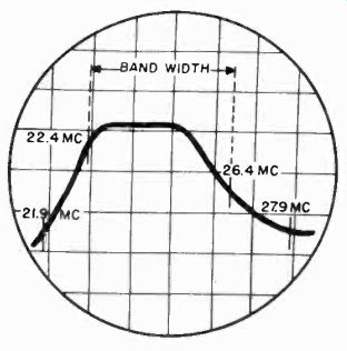
Figure 46. Video IF response curve using tuned circuits only.
A parallel resonant sound trap presents a high impedance to the signal for which it is tuned. Thus, when inserted in the grid Figure 47. Simplified circuit of f-f amplifier with grid wave trap.
circuit of an amplifier, as shown in Figure 47, it is in series with the signal path and effectively blocks the unwanted sound IF signal. Since the trap is very sharply tuned, it does not reject the desired frequencies. A second trap is usually incorporated in the next stage to attenuate the adjacent channel audio carrier signal at 27.9 Mhz.
Cathode wave-traps are also used to reject unwanted signals.
When inserted in the cathode of a video IF amplifier stage (Figure 48), a trap is in series with the input signal and prevents the amplification of the sound carrier and its associated side bands.
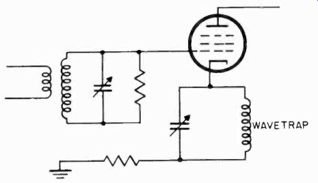
Figure 48. Simplified circuit of IF amplifier with cathode wave trap.
Sound traps usually consist of a fixed capacitor and a slug tuned coil, which can be adjusted to resonate at the correct frequency. They are often pre-tuned and sealed at the factory, so that they require no further adjustment. In some cases, they must be aligned whenever the video IF amplifiers require servicing.
With the sound traps properly tuned, the overall video response curve of a receiver should be similar to that shown in Figure 49. This is the ideal wave shape, for it contains only the video signals.
3-30
Overcoupled I-F Amplifier with Wave Traps. The G.E. Model 801 receiver is an example of a design using an over coupled IF amplifier with wave-traps. See Figure 50. Three 6AC7 tubes are used in the three-stage video IF amplifier. The transformers T-1, T-2, T-3, and T-4 are over-coupled and loaded with resistor to obtain a response curve 4 Mhz wide. This type of circuit does not result in sufficient attenuation of the associated sound carrier or the adjacent channel sound carrier.
A suitable response curve is obtained in the circuit of Figure 50 by the addition of wave-traps. A third winding is added to each video transformer and tuned to trap out the audio carrier and its associated sidebands. The trap in T-1 is tuned to 27.9 Mhz to provide rejection at the adjacent channel audio 1.f., while the traps in T-2, T-3, and T-4 are tuned to 21.9 Mhz, the audio i.f. in the channel being received. The combination of sound traps 21.9 mhz and over-coupled transformers results in the response curve shown in Figure 51.
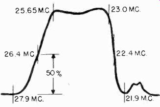
Figure 51. Response curve of IF amplifier channel using over coupled transformer
and sound traps.
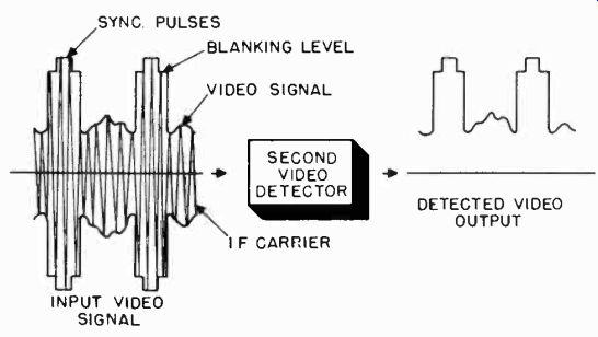
Figure 52. Input and output waveforms of the second detector.
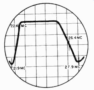
Figure 49. Response curve of video IF amplifier with sound traps properly
tuned.
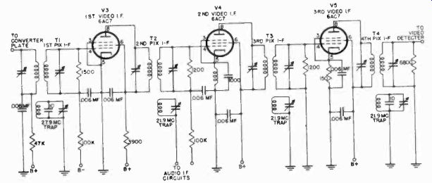
Figure 50. Overcoupled IF amplifier with wavetraps.
Wavetraps are inserted in the RCA circuit shown in Figure 41 in the following manner: The first three traps form absorption circuits. The first trap (T-1 secondary) is tuned to the associated sound IF frequency. The second trap (T-2 secondary) is tuned to the adjacent channel sound IF frequency. The third trap (T-3 secondary) is tuned to the adjacent channel picture carrier frequency. The fourth trap (T-4 secondary) is in the cathode circuit of the fourth picture IF amplifier, V-4, and is tuned to the associated sound carrier IF frequency. The primary of T-4, in series with the resistor and capacitor, forms a series resonant circuit at the frequency to which L-2 is tuned (23.4 Mhz). This provides a low impedance cathode circuit at 23.4 Mhz, permitting the tube to operate at high gain. At the resonant frequency of the secondary of T-4 (21.25 Mhz), the wavetrap acts as high impedance in the cathode circuit and greatly reduces the gain of the amplifier. The 21.25 Mhz audio IF signals are therefore attenuated.
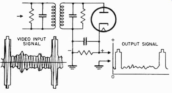
Figure 53. Diode detector and waveform.
3-31 The Video Second Detector. The amplified video IF signal passes from the last IF amplifier to the second video detector, which demodulates the carrier leaving the video, blanking, and synchronizing information. The wave form of the signal at the output of the detector is shown in Figure 52. At the present time, all television receivers utilize diode detectors as shown in Figure 53. This detector is similar to that used in the ordinary superheterodyne receiver, except that it must pass a wider band of frequencies and maintain the proper polarity of the video signal.
3-32 Signal Polarity. When a signal passes through a vacuum tube, a 180-deg phase shift takes place, and as a result, the polarity of the signal is reversed. In ordinary sound receivers, the polarity of the signal at the speaker is not important. In television receivers, the video signal must be of the proper polarity, otherwise a negative picture will be obtained on the screen of the picture tube, as shown in Figure 54. The proper polarity to obtain a positive picture depends upon whether the signal is fed to the grid or to the cathode of the picture tube. The correct polarity when the video signal is applied to the grid of the picture tube is shown in Figure 55a. The polarity must be reversed if the signal is fed to the cathode of the picture tube, as shown in Figure 55b. Since the polarity of the signal is reversed each time it passes through a stage, the number of stages in the receiver, following the video detector, determines the polarity of the signal at the picture tube.
3-33 Positive and Negative Detectors. A modulated IF carrier contains identical positive and negative picture information above and below the a-c axis. When a diode detector is connected as shown in Figure 53, a positive detected signal results.
This is because the signal above the a-c axis drives the plate of the diode positive with respect to the IF signal ground, and the diode conducts, whereas the signal below the a-c axis does not cause the diode to conduct.
By reversing the plate and cathode connectors, as shown in Figure 56, the signal below the a-c axis may be detected, giving a polarity opposite that obtained with the circuit shown in Figure 53.
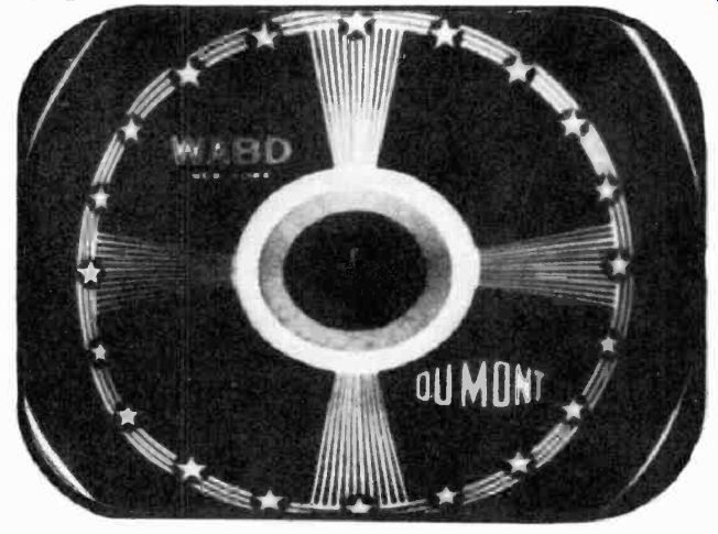
Figure 54. Test pattern showing negative picture caused by improper polarity
of grid of picture tube.
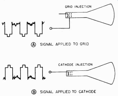
Figure 55. Polarity of signal required at grid and cathode of picture tube.
3-34 Detector Frequency Response. The frequency response of the second detector should be linear up to 4 or 5 Mhz. Slightly above these frequencies, the response of the detector should fall off sharply to attenuate the IF carrier and the harmonics produced by distortion in the detector. In older receivers which used an RF frequency of 12.75 Mhz, the ratio of the IF carrier frequency to the highest video frequency was 3 to 1. With this small ratio, it was difficult to separate the 4 Mhz video band from the intermediate frequency signal. It was necessary to add a number of band pass filters to obtain good frequency response over the 4 Mhz video band and at the same time attenuate high frequency signals. The new video IF frequency of 26.4 Mhz has simplified the problem somewhat, although filter circuits are still used to maintain optimum frequency response.
Figure 57 shows a complete video detector incorporating a band pass filter. The diode load resistance, R-1, is very low (3,300 ohms compared to the 2 megohms found in ordinary circuits). This low value of load resistance permits the detector to pass a wide band of frequencies. L-1 and L-2 constitute a band pass filter whose upper limit is approximately 5 Mhz. Higher frequencies are greatly, attenuated by L-1 and L-2, and in addition are by-passed by capacitor C-1.
While a low value of load resistance used in a detector results in the required wide frequency response, it reduces the efficiency of the detector. As a result, the output of the signal obtained is but 1 or 2 volts. This signal is not of a great enough amplitude to properly drive the picture tube. In order to bring the signal up to the required level, it is passed through a number of video amplifier stages.
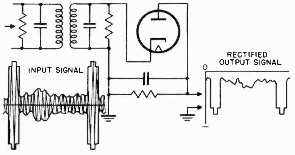
Figure 56. Diode detector and waveform.
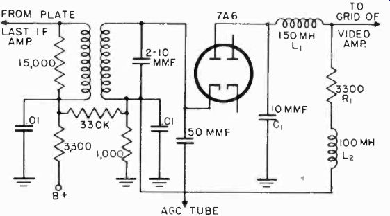
Figure 57. Schematic of video detector with bandpass filter.
3-35 Direct-Coupled Video Detector. The d-c component of the detected video signal is proportional to the average brightness of the transmitted scene. When passed through an ordinary amplifier, the d-c component of a signal is lost. In a television receiver, the d-c component must be maintained in some way so that the average brightness of the transmitted scene will be conveyed to the picture tube. One method used to accomplish this is through the use of a direct-coupled video detector and video amplifier. Direct-coupling passes on the d-c component which would normally be lost in other circuits. The G.E. Model 801 receiver uses the direct-coupled video detector shown in Figure 58.
The video IF signal is transformer-coupled to the cathode circuit of the detector. A negative signal is developed across the 1,500 ohm diode load resistor, R-1. L-1, C-1 and the input capacity of the video amplifier together comprise a band pass filter.
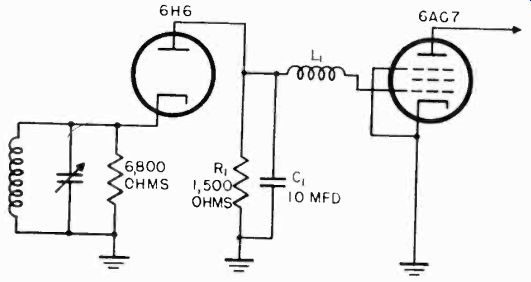
Figure 58. Direct coupled video detector.
The filter is direct-coupled to the grid of the video amplifier, and the d-c voltage drop across R-1 provides grid bias for the video amplifier.
3-36 Push-Pull Detectors. A signal somewhat greater than that available from a regular diode detector can be obtained through the use of a push-pull detector. The circuit of a pushpull detector is shown in Figure 59. The video IF signal is fed to the plates of a dual diode through a balanced transformer.
The cathodes of the dual diode are tied together. The operation of this detector is identical to that of a full-wave rectifier. One diode conducts the positive portion of the IF signal, and the other, the negative portion. The detected signal is developed across the diode load resistor, R-1, and is of positive polarity.
3-37 Video Amplifiers. The function of the video amplifier in a television receiver is similar to that of an audio amplifier in an ordinary sound receiver.
In a sound receiver, the signal at the output of the second detector is not great enough to drive the loudspeaker, and must be passed through one or more stages of audio amplification before being applied to the speaker.
In a television receiver, the signal at the video second detector is not of sufficient amplitude for proper operation of the picture tube. It is passed through the video amplifying stages to bring it up to the necessary amplitude. As mentioned previously, the signal at the output of the last video amplifier must be of a pre-determined polarity. This polarity is determined by whether or not the signal is fed to the grid or cathode of the picture tube.
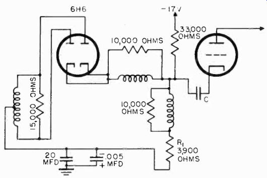
Figure 59. Push-pull video detector.
FREQUENCY

Figure 60. Response curve of video amplifier.
3-38 Frequency Response. The video amplifier should have a frequency response uniform from approximately 30 cycles to 4 Mhz, as shown by the curve of Figure 60. Ordinary resistance-capacitance coupled amplifiers, such as shown in Figure 61, cannot provide this frequency response characteristic, since at high frequencies, the interelectrode capacity of the tube bypasses the signal to ground, while the coupling capacitor Cc has a large enough reactance to block some of the low frequency output voltage.
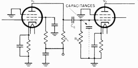
Figure 61. Simplified schematic of resistance coupled amplifier.
3-39 Phase Distortion. When a signal is passed through an amplifier, it is delayed slightly. This delay usually varies with the frequency of the input signal, and when signals of more than one frequency are fed into an amplifier, the amount of delay is different for each frequency. This difference in delay is referred to as phase distortion. Phase distortion of the video signal will cause the picture to appear smudged and blurred, as shown in Figure 62. This type of distortion must be kept to a minimum.
3-40 High Frequency Compensation. The capacitance between the various elements of a video amplifier circuit and ground tend to reduce the high frequency response of the amplifier. To keep these shunting capacities to a minimum, circuit components must be carefully placed, lead lengths kept short, and low loss tube sockets used. Video amplifier tubes, such as the 6AC7 have been carefully designed to give a minimum of interelectrode capacity. When all these precautions have been taken, the shunting capacity will still be 20 to 30 mmf. This capacity is great enough to cause appreciable loss of high frequency response.
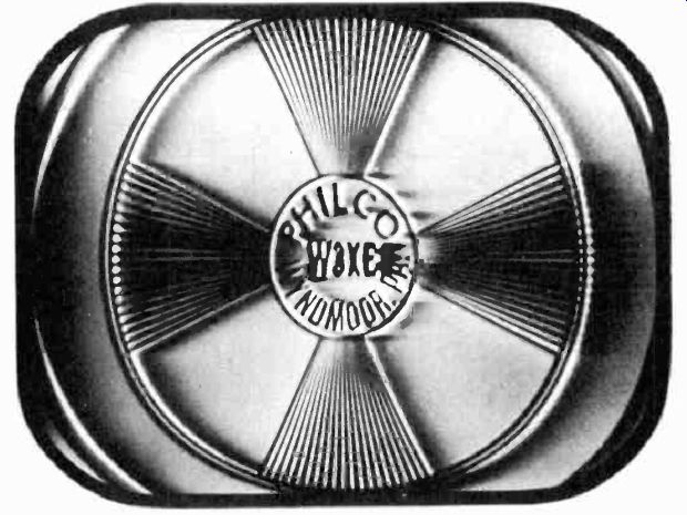
Figure 62. Test pattern showing effect of phase distortion.
To compensate for this loss, an inductance may be placed in series with the load resistor of an amplifier, as shown in Figure 63. The value of this inductance is so chosen, that at low frequencies its effect is negligible. At high frequencies, the inductive reactance becomes great enough to increase the load resistance of the amplifier. The point at which the impedance of the inductance begins to increase the effective load resistance corresponds to the frequency at which the response of the amplifier begins to fall off due to the shunting capacitance. The increased load resistance gives a greater voltage drop and a resulting greater output voltage, which compensates for the drop caused by the shunting capacitance. This method of high frequency compensation is referred to as shunt-peaking.
The effects of shunt capacitance may also be compensated for by adding an inductance in series with the output coupling capacitor, or an amplifier, as shown in Figure 64. The coupling capacitor, Cc, and the inductance form a series resonant circuit. This method, referred to as series-peaking, is more desirable than shunt-peaking, since it permits the use of a slightly higher load resistance which gives greater gain. Phase distortion with series-peaking is less than with shunt-peaking. In some designs, a combination of series and shunt-peaking is used, as shown in Figure 65, to obtain the required video amplifier response characteristic.
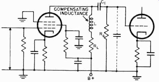
Figure 63. Shunt-peaking frequency compensation.
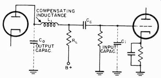
Figure 64. Series-peaking frequency compensation.
The gain of an amplifier stage is proportional to its load resistance. If the load resistance is increased, the gain of the amplifier increases. The maximum gain obtainable is limited by the fact that increased load resistance causes a loss in high frequency response. The effect of increased load resistance on the frequency response of an amplifier is shown in Figure 66.
Since high frequency response is important in video amplifiers, low values of load resistance, sometimes as little as 1,000 ohms, are often used. As a result, a stage gain of about 20 is obtained. With a gain of this order, a single video amplifier stage is sufficient, providing at least a 2 volt signal is available at the output of the second detector. An output signal of lesser amplitude necessitates an additional stage of video amplification before the picture tube.
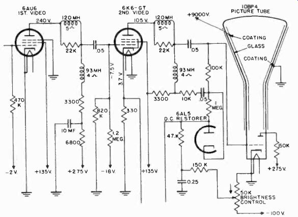
Figure 65. Two stage video amplifier suing shunt and series peaking.
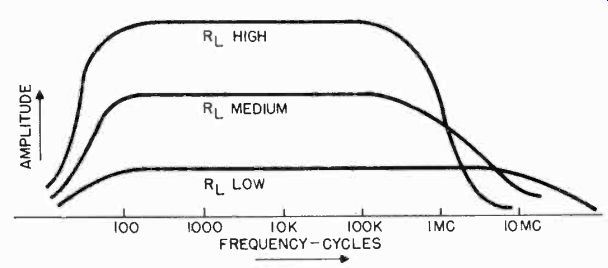
Figure 66. Effect of different load resistances on the response of resistance
coupled amplifier.
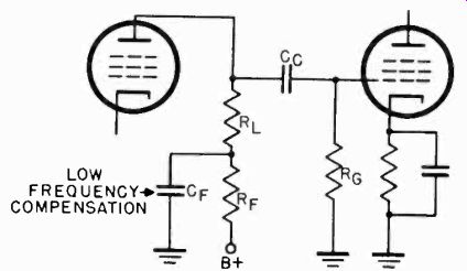
Figure 67. Parallel resistor-capacitor combination for low frequency compensation.
3-41 Low Frequency Compensation. At low frequencies, the reactance of the video amplifier output coupling capacitor is great enough to cause a loss in low frequency response. This loss occurs because the coupling capacitor forms a voltage divider with the grid resistance of the picture tube. One way to eliminate this effect is by increasing the value of the capacitor to reduce its reactance at low frequencies. While a comparatively high capacitance may be used, a value which entirely eliminates loss of low frequency response will also increase stray capacitance to a value which will effect the high frequency response. Additional reduction in low frequency attenuation may be obtained by making the picture tube grid leak resistor as large as feasible.
After the above precautions have been taken, any remaining low frequency attenuation is removed by a parallel resistor-capacitor combination, placed in series with the plate load resistor of a video amplifier, as shown in Figure 67. The values of the resistor and capacitor are chosen so that they will increase the impedance of the plate circuit at low frequencies. The increased plate circuit impedance results in a greater voltage gain, compensating for low frequency attenuation. The effects of the resistor-capacitor combination are negligible at high frequencies, since the capacitor, Cf, acts as a short circuit across resistor Rf.
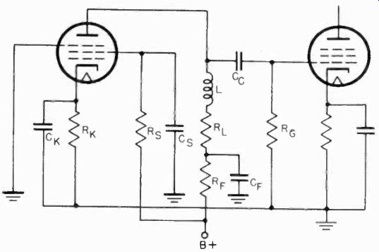
Figure 68. Video amplifier with high and low frequency compensation components.

Figure 69. Composite video signal at the output of the video detector.
Figure 68 shows the circuit of a video amplifier with both low and high frequency compensating elements.
3-42 D-C Restoration. As has already been pointed out, the output of the video detector has a d-c component which determines the average brightness of the scene appearing on the screen of the picture tube. This d-c component is combined with the a-c components of the picture information. Figure 69 shows the video signal at the output of the video detector. When this signal is applied to the grid of the picture tube, all signals which reach or go below the black level drive the grid to cutoff.
Signal levels above the black level extend as high as the white level. Between the black level and the white level are the signal levels which correspond to shades of grey.
In order to reproduce a picture in the proper shades of black, grey, and white, one of the shades must remain fixed, so that it can serve as a reference for all the other shades. The television signal has one component which is always constant. This is the top of the blanking pulse, which is always equal to the black level. If the tops of the blanking pulses are made to equal the cutoff bias of the picture tube, all signals above the blanking pulse level will swing the picture tube grid more positive and produce shades of grey on the screen.
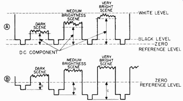
Figure 70. A, video signals of three different screen brightness levels.
B, video signals with d-c component removed.
Consider now what happens when the video signal shown in Figure 69 is passed through an amplifier. The d-c component is blocked by the coupling capacitors of the a-c amplifier. With the d-c component removed, the video signal centers itself above and below the zero reference level, so that as much area of signal is above as is below this level. Under these conditions, the blanking pulses will no longer occur at the black level. Without a fixed black level, some of the blanking pulses occur above the grid cutoff bias and, therefore, do not blank out the return traces. It is apparent that some means must be provided for reinserting the original d-c level of the signal. Just how much d-c voltage must be reinserted depends upon the original video signal. Figure 70A illustrates several different video signals representing varying levels of average scene brightness. In a dark scene, the d-c component is relatively small. The d-c component is greater for a scene of medium brightness, and rises still further for a very bright scene. When these video signals are passed through an a-c amplifier, they center themselves around the zero reference level, as shown in Figure 70B. In order to hold the blanking pulses of all three signals at the same level, a d-c component equal to "a" volts must be added to the dark scene, "b" volts to the medium brightness scene, and "c" volts to the very bright scene. These d-c components are obtained by feeding the signals to a circuit known as a d-c restorer. A d-c restorer employs a diode which rectifies the portion of the signal below the zero reference axis and derives a d-c signal from the rectified voltage.
3-43 Diode Restorer Circuits. A d-c restoration circuit using a diode is shown in Figure 71. The video signal from the video amplifier is coupled to the grid of the picture tube through C-2.
Across the output of the video amplifier is the d-c restoration circuit, consisting of V-2, C-1, R-2, and R-3. At the plate of the video amplifier, there is no d-c component in the signal.
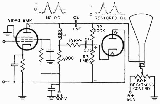
Figure 71. Schematic of diode d-c restorer.
However, at the picture tube grid, the d-c component has been restored by the diode circuit. The operation of the d-c restorer is as follows:
1. When the video signal swings positive, the cathode of the diode is driven positive with respect to its plate, and it does not conduct. On the negative portion of the signal, the cathode becomes negative with respect to the plate, and the diode conducts.
2. Current flows through R-2 and R-3 to C-1, and charges the condenser to a voltage equal to the amount that the sync tips are below the zero reference axis.
3. The d-c voltage built across C-1 is equal to the voltage difference between the sync tips and the desired reference level.
4. The d-c voltage appears across R-2 and R-3 and is applied to the grid of the picture tube.
5. The added d-c component maintains the level of the blanking pulses at the desired reference, or black level.
With this circuit, an increase in the portion of the video signal below the zero reference level causes an increase in the d-c voltage developed across C-1. Thus, as the scene brightness changes, a varying d-c voltage is developed which maintains all blanking pulses at the same level.
It is important to note that the d-c voltage changes each time the video signal varies due to actual changes in scene brightness.
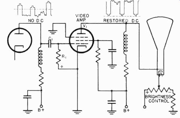
Figure 72. D-C restoration in the video amplifier stage.
The time constant of C-1 and R-2, R-3 is chosen so that C-1 will hold its d-c charge between two successive sync pulses.
The time constant is, however, small enough so that when the transmitted scene brightness changes, C-1 is able to charge or discharge to the voltage corresponding to the new brightness level.
3-44 Video Stage Restoration. D-C restoration can take place in the video amplifier itself if the amplifier circuit is arranged as shown in Figure 72. The signal is fed from the video detector to the video amplifier through coupling capacitor C-1. The d-c component cannot pass the coupling capacitor and does not appear on the grid of V-1. When the video signal swings above the zero reference level, the grid becomes positive and draws current which charges C-1. This charge is the d-c component to be reinserted. R-1 is large enoughtopreventC-1 from discharging between successive sync pulses. The d-c component which now appears on the grid of V-1 is amplified with the other components of the video signal. The composite signal, including the d-c component appears at the plate and is coupled directly to the grid of the picture tube. No coupling capacitor is used between the video amplifier and that picture tube, because it would block the restored d-c component.
3-45 The Brightness Control. The manner in which the d-c restorer circuit holds all the blanking pulses at a constant level has just been described. In order to blank out the return trace, the beam in the picture tube must be cut off when the blanking pulses reach the black level. If this condition exists, the sync pulses, which are more negative than the blanking pulses, will not appear in the picture. The voltage on the grid of the picture tube must therefore be adjusted so that the grid is biased to cutoff, which corresponds to the black level.
A circuit commonly used to provide for adjustment of the picture tube's grid bias is shown in Figure 73A. A positive voltage is applied to the cathode through the variable resistor R2.
Also shown in the circuit is a video amplifier V1, direct coupled to the grid of the picture tube. D-C restoration takes place in the grid circuit of V1 through the action of R1 and C1. The plate voltage on V1 is lower than the voltage on the cathode of the picture tube. Since the grid of the picture tube is directly coupled to the plate of V1, it is negative with respect to the cathode. The negative grid bias can be varied by changing the setting of R2. R2 is adjusted for a negative bias which just cuts off the beam current. This setting corresponds to the black level. Once the bias has been adjusted in this manner, the d-c restoration circuit automatically holds the blanking pulses at the cut-off bias. R2, which initially sets the grid bias, is the brightness control of the receiver.
When this control is properly adjusted, the video signals which are more positive than the black level will permit the beam to pass to the screen and reproduce the shades of the picture being received.
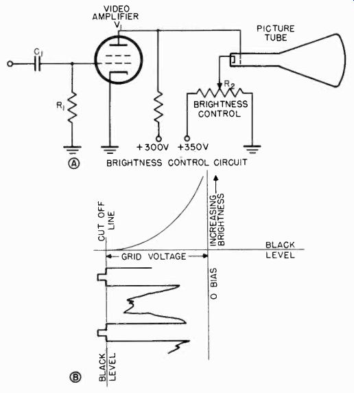
Figure 73. A, circuit for providing adjustment of picture tube bias. B, effect
on picture brightness of variations in grid voltage.
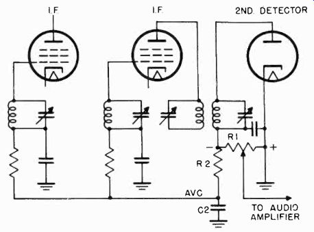
Figure 74. Simplified schematic of a.v.c. circuit of AM receiver.
Figure 73B shows how the setting of the brightness control affects the illumination on the picture tube. The bias is adjusted so that all signals to the left of the black level are beyond the cutoff voltage of the picture tube. The video signals to the right of the cutoff bias increase the brightness as they swing toward zero bias voltage.
3-46 Automatic Gain Control. Automatic gain control in a television receiver is similar to automatic volume control in ordinary broadcast receivers. Its purpose is to maintain the intensity of the picture at a constant level despite variations in the average strength of the received signal. The effect on the picture of a fading television signal is more drastic than the effect of a fading audio signal upon the output of a sound receiver. A fading signal will cause changes in the intensity of the picture, and if of sufficient amplitude, will effect the stability of the picture, because the sync level for which the receiver has been adjusted will not be maintained.
3-47 Automatic Volume Control. While the automatic gain control system used in television receivers differs considerably from the automatic volume control circuits found in sound receivers, a review of the operation of "a.v.c." will make an excellent background for an understanding of "a.g.c.". Figure 74 is a simplified schematic diagram of the a.v.c. circuit of an ordinary receiver.
The diode detector rectifies the signal at the output of the last IF transformer. The audio voltage appearing in the output of the detector contains a d-c component whose amplitude is proportional to the strength of the carrier. This d-c component is used to control the gain of the IF amplifiers. In order to separate the audio and d-c components, capacitor C2 is connected from one side of the decoupling resistor R2 to ground. As a result, only the d-c component is left at the point marked a.v.c.
When the carrier strength increases, greater negative voltage is developed across R1, and is fed back to the grids of the IF amplifiers, where it constitutes negative bias. The IF amplifier tubes are remote cut-off pentodes whose gain decreases with increased bias. When the carrier strength decreases, the negative bias on the IF amplifiers decreases, and the gain of the IF amplifiers increases, compensating for the drop in signal strength. If the by-pass condenser, C-2, were not present in the circuit, the gain of the IF amplifier would be controlled by the audio signal and not by the average carrier strength, as happens when C2 is in the circuit.
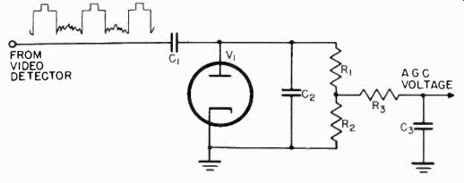
Figure 75. Simplified diagram of a.g.c. circuit.
3-48 Automatic Gain Control Circuits. The d-c component of the video signal cannot be used for gain control bias, as is done with the d-c component of the sound signal in ordinary receivers. This is so because the average carrier voltage of the television signal represents the brightness of the scene. If the d-c component were used as a gain controlling bias, it would maintain the scene brightness at a constant level, regardless of whether the scene were in daylight or at night. A signal, if used for a.g.c., must be proportional to the maximum carrier strength of the television signal only. It must have no relation to the brightness of the scene. The sync signal fills these requirements. It represents 100% modulation of the carrier and has no relation to the brightness of the scene. When the carrier fades, the level of the sync signal changes, at which time the automatic gain control system increases the gain of the receiver.
A simple a.g.c. circuit is shown in Figure 75. A portion of the video detector output is coupled through C1 to the plate of the a.g.c. rectifier tube V1. The diode conducts because of the positive polarity of the signal applied to its plate. Current flows and charges capacitor C-2 to the peak value of the sync signals.
This charge cannot leak off readily because of the long time constant of the circuit formed by C2, R1, and R2. The time constant is set to equal the time duration of about 10 horizontal lines. The voltage across C2 therefore remains constant and equal to the peak value of the sync signals. This voltage is tapped between R1 and R2 and is the a.g.c. signal. When the level of the sync signals decreases for a period of time equal to more than ten horizontal lines, the voltage across C2 drops, and a compensating a.g.c. voltage is applied to the amplifiers under control.
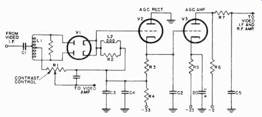
Figure 76. Delayed a.g.c. circuit.
A more complex a.g.c. circuit is shown in Figure 76. The video IF signal is coupled through C1 to the full-wave video detector V1. The detected signal appears across resistor R2.
Rectified voltage appearing at the cathode of V1 is directly coupled to a.g.c. rectifier V2. When V2 conducts, capacitor C2 charges to the peak value of the sync signals.
As in the previous a.g.c. circuit, the time constant of the network consisting of C2, R3, and R4 is long, and C2 holds its charge for a period equal to several horizontal lines. Since the charge on C2 is equal to the peak value of the sync signals, it serves as the a.g.c. voltage. This voltage is fed to the grid of V3, which amplifies the a.g.c. signal.
The grid of the a.g.c. amplifier is connected to a negative 33 volt source and the cathode to a negative 23 volt source. The grid is therefore 10 volts negative with respect to the cathode.
This negative bias is sufficient to cut off the tube when no signal is reaching it from the detector. When signal is present, the amplifier does not conduct unless the signal voltage is high enough to overcome the cutoff bias. Thus, a.g.c. action is delayed. Delayed a.g.c. action is desirable when the signal is weak.
The delay permits the IF amplifiers under control to operate at full gain until the input signal reaches a predetermined level.
On very weak signals, there is no a.g.c. action, and the amplifiers operate at full gain.
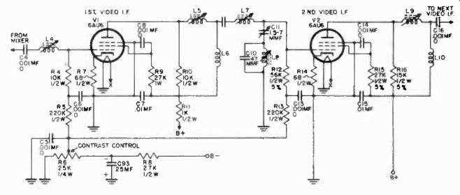
Figure 77. Gain control by varying the grid bias 'on remote cutoff pentode
IF amplifiers.
The plate load resistor of V3, (R6), is connected to a negative 2 volt source. The plate of V3 is therefore 21 volts positive with respect to its cathode. When a sufficiently strong signal appears at the grid of V3, the tube conducts and a potential is developed across resistor R6. This voltage is fed through the isolating network, R7-05, to the grids of the video and RF amplifiers.
3-49 A.G.C. vs. Contrast Control. To avoid confusion, the functions of a.g.c. and the contrast control should be clearly understood. The contrast control varies the gain of the receiver to obtain the relative brightness of light and dark areas in the picture, as desired by the viewer. Once this control has been adjusted, it remains fixed, and the receiver maintains the same picture contrast as long as its input signal level remains the same.
A change in the amplitude of the signal at the antenna terminals of the receiver will result in a change in contrast. When a change in signal strength takes place, the a.g.c. circuit functions to change the gain of the amplifier circuits and return the contrast to its preset value.
There are several points in a receiver where a variable contrast or gain control can be inserted. In the circuit of Figure 76, the video detector load resistor, R1, is made variable and provides a means for adjusting the input voltage of the video amplifier.
Figure 77 illustrates another method of controlling the gain of a receiver. Here the grid bias of two of the IF stages is made variable. Since the IF amplifier tubes are remote cut-off pentodes, variation of their grid bias varies the gain of the tubes.
THE SWEEP CIRCUITS
3-50
So far, those circuits of a television receiver which select and amplify the video signal and bring it up to a level sufficient to drive the grid of the picture tube, have been described.
Not yet covered are these circuits which control the motion of the electron beam and cause it to trace out a picture in exact synchronism with the picture being scanned at the television station. These circuits are known as sweep circuits.

Figure 78. Block diagram of vertical and horizontal sweep circuits.
Figure 78 is a block diagram of the vertical and horizontal sweep circuits, showing the path of the signal from the video detector to the deflecting plates or coils. At the output of the detector, the composite video signal carries both the picture information and the synchronizing pulses. These parts of the video signal are shown in Figure 79. The picture information is applied to the grid of the video amplifier, to be passed on to the picture tube, while the synchronizing pulses must be separated and directed to the sweep oscillators. This separation of the sync pulses is known as clipping and is generally accomplished, by a properly biased diode or triode, connected to the output of the video detector.
The separation of the sync signals may also take place after the video amplifier stage. In this way, the need for a separate sync amplifier is avoided.
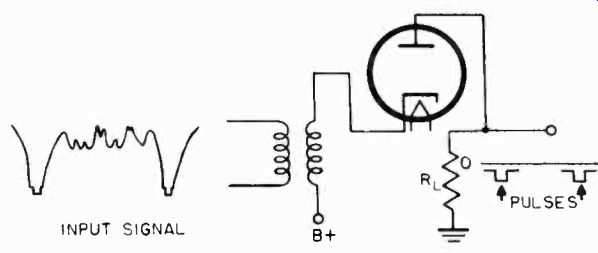
Figure 80. Diode sync clipper.
3-51 Diode Sync Clippers. A simple diode sync clipper is illustrated in Figure 80. The diode cathode is positive, so that current cannot flow until a negative voltage is applied between cathode and ground. The amplitude of the negative voltage necessary to cause the diode to conduct is determined by the positive cathode voltage. The cathode voltage is positive enough to keep the diode from conducting the picture signal and the blanking pulses. When a sync pulse appears at the cathode of the diode, the diode conducts because the amplitude of the pulse is greater than the bias on the positive cathode of the diode.
The output voltage obtained across the diode's plate resistor contains only the sync pulses as shown in the figure. If the detected signal is of the opposite polarity, the diode is reversed, and a negative voltage applied to the plate to control the voltage level at which the diode conducts.
In the circuit of Figure 81, the diode is self-biased and does not require a separate d-c voltage source. Values of R and C, connected between the cathode of the tube and ground, are chosen to give a time constant equal to the interval between horizontal pulses. The condenser is charged by successive sync pulses, and develops a voltage across the resistor which biases the diode to the level of the blanking pulses. The diode conducts only when the sync pulses, which are of greater amplitude, are applied to the circuit.
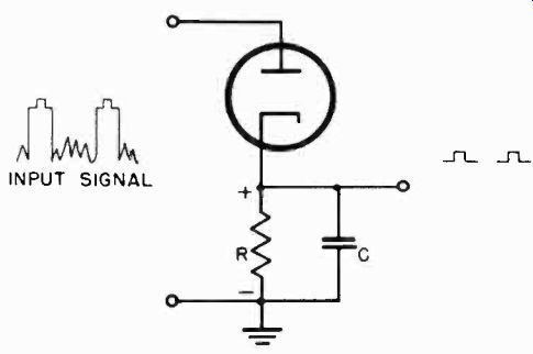
Figure 81. Seil-biased diode sync clipper.
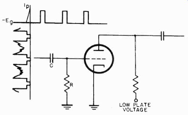
Figure 82. Simplified schematic of triode sync clipper.
3-52 Triode Clippers. The chief advantage of the triode clipper over the diode type is the amplification which takes place in conjunction with the clipping action. A triode clipper and the sync signal in its output are shown in Figure 82. The constants of R and C are chosen so that a negative bias, sufficient to cause cutoff, is developed on the grid. The bias necessary to cause cut-off is low, because the tube is operated at a low plate potential.
As shown in Figure 82, the blanking level is equal to the cutoff bias. Signals of lesser amplitude are removed, while the sync pulses, which are of greater amplitude, are amplified and appear inverted in the output of the triode.
In many receivers, a stage of sync amplification follows the separator, and at times a second sync separator is used to remove noise pulses superimposed on the sync signal. Figure 83 shows a circuit using two sync separators. The first sync separator stage clips the video information and reverses the polarity of the signal. This stage operates at low plate voltage to provide a low cutoff bias which removes all signal information above the blanking level.
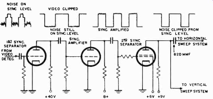
Figure 83. Cascade sync clipper.
The clipped sync signal, appearing in the output of the first separator, is "clean" on one level, but has noise pulses modulating the other level. The signal is then fed to an amplifier which reverses its polarity, so that it is again negative. The operation of the second sync separator should not be confused with that of the first sync separator. The second sync clipping stage is a tetrode operated with a low plate voltage and a relatively high screen voltage. It is grid leak-biased. Under these conditions the plate voltage is lower than the screen voltage, and the tube has a dynatron characteristic. It removes the tops and bottoms of the synchronization pulses. Thus, the noise pulses are removed from one level of the sync signal and any remaining picture components are removed from the other level.

Figure 84. Integrating circuit.
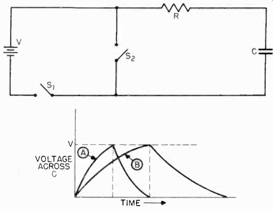
Figure 85. Operation of integrating circuit.
3-53 Vertical Sync Segregation. After the sync pulses have been removed from the composite signal, it is necessary to segregate the 60 cycle vertical sync pulses and the 15,750 cycle horizontal sync pulses. Segregation of the vertical sync pulses is accomplished by applying the combined sync signals to a filter network of the type shown in Figure 84. This network is known as an "integrating" circuit. It consists of a series resistance and capacitance, with the output taken from across the capacitance.
Figure 85 shows how an integrating circuit distinguishes the vertical sync pulses from the horizontal sync pulses. In the figure, a battery and switch are connected across an integrating circuit. Operation is as follows:
1. When the battery switch, S1, is closed, a current flows in the circuit and charges the capacitor C through resistor R. The capacitor continues to charge until it reaches the voltage of the battery.
2. If the battery switch, S1, is now opened, and the shunting switch, S2, closed, the charge on. the capacitor will leak off through resistor R.
3. The time that it takes to charge the capacitor is exactly equal to the time it takes to discharge the capacitor. The voltage across C during the "charge" and "discharge" intervals is shown in curve A. The charging and discharging time depends on the values of R and C. The larger the values of R and C, the longer it takes to charge and discharge the capacitor.
4. Suppose now, a capacitor with twice the capacitance is substituted for C in Figure 85. The charge and discharge voltages across the capacitor will now appear as shown in curve B. Note that by doubling the capacitance of C, the charge and discharge time is also doubled. Similarly, if C remains the same and R is doubled, the charging time will be doubled, and the voltage across the capacitor would again appear as in curve B. The time it takes to charge and discharge a capacitor in series with a resistor, therefore, depends upon the values of each. The time required to charge the capacitor to 63.2% of the voltage applied to the circuit is known as the circuit's "time constant". The value of the time constant, expressed in seconds, is the product of R and C. For example, if a 0.1 microfarad capacitor is placed in series with a 1 megohm resistor, it will take 0.1 of a second for C to reach 63.2% of the applied voltage.
The importance of the time constant (RxC) in the integrating circuit can now be understood. The RC time constant of the circuit is made much longer than the duration of the horizontal sync pulses, which last for about 5 microseconds. When combined synchronizing signals, such as shown in Figure 86, are applied to an integrating network with a time constant of approximately 45 microseconds, the following action takes place:
1. The horizontal sync pulse, which lasts only 5 microseconds, causes the capacitor to charge only slightly (1 and 2 Figure 86B). When the pulse ends, the charge across the capacitor leaks off through resistor R.
2. The equalizing pulses, which last for 2.5 microseconds, create negligible charges (3 in Figure 86B) across C, because the time constant of the circuit is 45 microseconds.
3. When the long duration serrated vertical sync pulse, which lasts for 190.5 microseconds, takes place, the capacitor has sufficient time to charge to the peak value of the applied voltage (in this case, the peak value of the vertical sync pulses).
4. The first serrated pulse charges the capacitor to a much higher level than the horizontal or equalizing pulses.
5. When the pulse ends, the charge starts to leak off through R.
6. Because of the long time constant of the circuit, the charge leaks off slowly during a short interval (4 in Figure 86) until the next serrated pulse occurs. The drop in voltage across C is therefore very small.
7. The second serrated pulse charges the capacitor further.
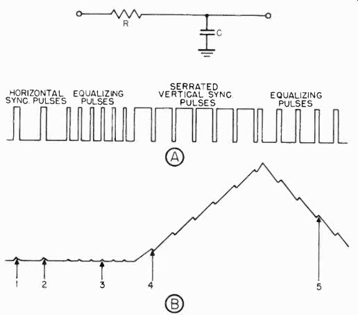
Figure 86. Input and output waveforms of integrating circuit.
Again, at the end of the pulse, the charge begins to leak off the capacitor until the third serrated pulse charges it still further.
8. The succession of serrated pulses charges C to the amplitude of the incoming sync pulses.
9. When the serrated pulses are completed, the capacitor begins to discharge.
10. During the discharge period, the six equalizing pulses occur, but their duration is too short to maintain the voltage on C. The notches appearing on the discharge portion of the curve (5 in Figure 86) are due to the slight charging effects of the equalizing pulses.
11. The pulse B of Figure 86 is a segregated vertical sync pulse which can now be used to synchronize the vertical sweep circuits.
The net effect of the integrating circuit is to separate the serrated vertical sync pulses from the horizontal sync pulses.
In some receivers, two or three integrating circuits are cascaded for improved integrating action. Such a circuit is shown in Figure 87.
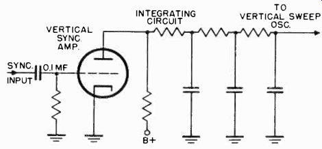
Figure 87. Cascaded integrating circuit.
3-54 Horizontal Sync Segregation. A circuit similar to an integrating network is used to separate the horizontal sync pulses from the combined sync signal. This circuit is known as a "differentiating" circuit, and is shown in Figure 88A. Two important differences distinguish this circuit from an integrating circuit. First, the RC time constant is much shorter, being about one fifth (1 microsecond) of the duration of the horizontal sync pulses. Second, the output is taken from across R rather than C. The following action takes place when the combined sync pulses shown in Figure 88B are applied to a differentiating circuit:
1. Since the time constant of the circuit is only 1 microsecond, the horizontal sync pulses, which last for 5 microseconds, have ample time to charge the capacitor to the peak voltage of the sync signals. When a horizontal sync pulse occurs, the current charging the capacitor through R rises very rapidly. During the charging period the voltage across R appears as in Figure 88C-1. At the end of the pulse the capacitor discharges very quickly through R, because of the small time constant of the circuit. During the discharge period current flows through R in a direction opposite that during the charge period. The voltage across R during the discharge period is as shown in Figure 88C-2. Hence, the voltage across R appears as a positive pulse when the capacitor charges during the rise time of the horizontal sync pulse, and then as a negative pulse when the same sync pulse ends. The voltage across R, when the horizontal sync pulses occur, is shown in Figure 88C.
2. The equalizing pulses, which last for 2.5 microseconds, also quickly charge and discharge C. Since the equalizing pulses occur at twice the frequency of the horizontal pulses, they produce positive and negative pulses across R at twice the frequency of those caused by the horizontal sync pulses.
3. When the serrated vertical sync pulse is applied to the differentiating circuit, C charges rapidly, and a positive pulse appears across R during the rise time of the serrated pulse.
The long duration serrated pulse holds the charge on C constant until the pulse ends. C then discharges rapidly through R, producing a negative pulse corresponding to the end of the serrated pulse. Each serrated pulse which follows has a similar effect on the differentiating circuit.
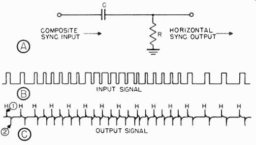
Figure 88. A, differentiating circuit. B, input and output waveforms of circuit
in A.
The output of the differentiating circuit, shown in Figure 88C, consists of differentiated vertical, horizontal, and equalizing pulses. All of these pulses are fed to the horizontal oscillator, but only those occurring at the horizontal sweep frequency affect the triggering of the horizontal oscillator. These pulses are marked H in the diagram. Note that all of these pulses are the same distance apart and that they occur right through the vertical blanking period. Thus the horizontal oscillator does not lose synchronization during the vertical blanking period.
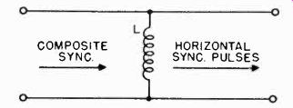
Figure 89. Inductive differentiating circuit.
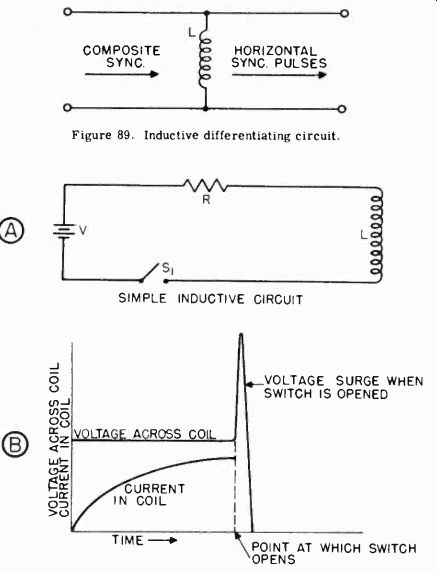
Figure 90. Operation of inductive differentiating circuit.
3-55 Other Differentiating Circuits. Another type of differentiating circuit, which is employed in many receivers, consists of an inductance placed in the plate circuit of the horizontal sync amplifier tube. Such a circuit is shown in Figure 89. This circuit's operation takes advantage of the fact that when the current in a coil is suddenly reversed, the voltage across the coil increases greatly. The principle is illustrated in Figure 90. When switch Si is closed, the current in the coil rises slowly, depending upon the inductance of the coil. The rising current in the coil builds up a magnetic field around the coil. When switch S1 is opened, the voltage across the circuit drops to zero.
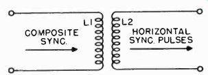
Figure 91. Transformer type differentiating circuit.
The magnetic field surrounding the coil collapses suddenly and induces a large voltage in the coil (Figure 90B). When a composite sync signal, such as shown in B of Figure 88 is applied to a coil type differentiating circuit, the voltage across the coil increases rapidly during the rise time of the horizontal, equalizing, and vertical sync pulses. At the end of a pulse, when its amplitude suddenly falls to zero, the magnetic field surrounding the coil collapses and produces a large voltage across the coil. The polarity of the voltage produced by the collapsing field is opposite that of the voltage produced during the rise period of a pulse. The rise and fall of pulses in the composite sync signal produces positive and negative voltages across the coil, similar to those produced by the RC circuit of Figure 88.
The differentiated sync voltages can be applied directly to the sync terminals of the horizontal oscillator if they are of positive polarity. If not, an amplifier must be provided for pulse reversal.
A two-winding transformer is sometimes used as a differentiating circuit, as shown in Figure 91. The primary acts as the differentiating circuit, while the secondary performs the task of coupling the differentiated pulses to the horizontal generator.
With a two-winding transformer, the secondary can be reversed, if need be, to produce positive sync pulses at the horizontal saw tooth generator.
3-56 Sweep Oscillators. The scanning of the mosaic in the camera pick-up tube was explained in Section 2. It was explained that the television picture is formed by the electron beam sweeping horizontally 15,750, and vertically 60 times per second.
This motion of the beam was the result of two sweep voltages which were applied to deflection plates mounted in the tube.
The sweep voltages were saw-tooth in shape. At the receiver, similar saw-tooth voltages are generated, which move the picture tube beam in step with that of the camera tube and help compose the final picture.
The saw-tooth voltages in the receiver are generated by charging a condenser with d-c voltage and then rapidly discharging it with a sharp pulse. The voltage across the condenser is the desired sawtooth waveform.
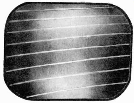
Figure 92. Raster pattern.
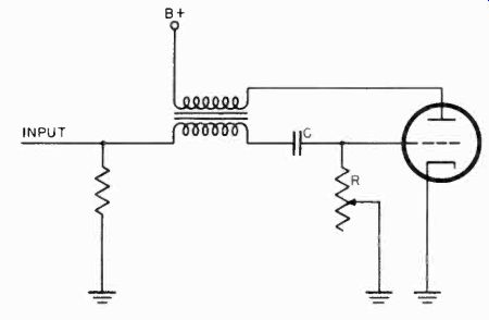
Figure 93.. Blocking oscillator circuit.
The sweep oscillators provide the sharp discharge pulse at the correct time, determined by the synchronizing pulses which maintain the oscillators at the same frequencies as the television station sync generator.
In the receiver there are two sweep oscillators, each of which is independent of the other. If vertical and horizontal sync pulses are not received to "lock in" the oscillators, they operate at their natural frequencies. Thus, discharge pulses are always provided for the saw-tooth generator circuit to form the pattern on the receiver screen known as the raster. A typical raster is shown in Figure 92. If the oscillators could not operate at their natural frequencies when no sync signal is being received, deflection voltages would not be generated, and the beam would form an intense spot at the center of the screen, causing a screen burn.
The two most common sweep oscillator circuits used in television receivers are the "blocking oscillator" and the "multivibrator"
3-57 The Blocking Oscillator. The circuit of a typical blocking oscillator is shown in Figure 93. It consists of a tube whose grid is transformer coupled to its plate. It operates as follows:
1. When the power supply potential is applied to the plate, current flows through the tube.
2. This current passes through the transformer winding which is in the plate circuit, causing a potential to be induced in the grid winding of the transformer.
3. The polarity of the induced voltage is such that the grid is made positive.
4. The positively charged grid causes an increase in the current through the tube and consequently through the plate winding of the transformer.
5. The increased current in the plate winding increases the potential induced into the grid circuit, causing further increases in plate current. The process continues until the tube reaches saturation.
6. During the process of increasing plate current, the capacitor in the grid circuit is charged.
7. When the tube reaches saturation, the current through the plate winding is no longer increasing and therefore there is no longer any induced voltage across the grid winding.
8. The absence of induced voltage permits the capacitor to discharge through resistor R, placing a negative potential on the grid. The negative potential reduces the current through the tube and through the plate winding.
9. The reduced plate current induces a potential across the grid winding, which increases the negative charge on the grid.
The process continues until the tube reaches plate current cutoff.
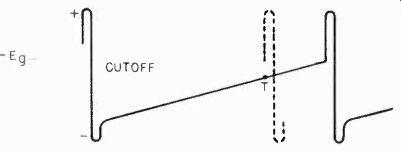
Figure 94. Grid voltage cycle of blocking oscillator.
10. During the decrease in plate current, the condenser C is charged, and when cutoff is reached, it discharges slowly through R, until the grid is no longer below cutoff and the cycle begins again.
The cycle of the grid voltage is shown in Figure 94. If a synchronizing pulse, which raises the grid voltage to a point where plate current can flow, is applied to the oscillator, it will "trigger" when the pulse is applied, rather than at its natural frequency as determined by the values of R and C. In Figure 94 a synchronizing pulse is applied at point T, which causes the oscillator to trigger as indicated by the dotted line. In this manner, the synchronizing pulses keep the blocking oscillator in step with the scanning motion occurring at the transmitter. The grid resistance R controls the natural frequency of the oscillator. It is commonly called the hold control, and is usually variable so that it can be adjusted for synchronization.
The blocking oscillator circuits of the vertical and horizontal sweep systems are essentially the same. The only differences are in the values of the resistor and capacitor in the grid circuit, which determine the frequency of oscillation. The oscillator transformers also differ slightly, the horizontal type having a lower capacity between windings to make it possible to obtain a sharp pulse at the horizontal frequency of 15,750 cps.

Figure 95. Horizontal sync pulse (1) is of sufficient amplitude to trigger
oscillator. Equalizing amplitude at (2) does not trigger oscillator because
of position on grid voltage curve.
Several points should be remembered regarding the operation of a blocking oscillator.
1. As illustrated in Figure 94, a blocking oscillator can be triggered before its natural frequency by a positive sync pulse which is sufficient to raise the bias voltage above cutoff value.
A negative sync pulse will drive the grid further beyond cutoff and continue to block the tube.
2. When the hold control R sets the natural oscillator frequency near the sync frequency, only sync pulses can trigger the oscillator. Equalizing pulses occurring between horizontal sync pulses are not of sufficient amplitude to affect the oscillator, since they occur too far down on the grid cutoff, as illustrated in Figure 95.
3. The negative pulses produced by a differentiating circuit cannot affect the operation of a horizontal blocking oscillator because they drive its grid further negative.
4. Positive pulses can be obtained from either the grid or plate circuits of a blocking oscillator.
3-58 The Multivibrator. The multivibrator type of oscillator consists of two triodes and a number of resistances and capacitances. Since no transformer is. necessary, this circuit is somewhat cheaper to construct than the blocking oscillator, and is therefore preferred where economy is a factor.
A typical multivibrator circuit is shown in Figure 96. When plate voltage is applied to the oscillator, the following actions occur:
1. The plate voltage of V2 is applied to C1.
2. C1 is charged and causes the grid voltage of V1 to rise.
3. The rise in grid voltage produces an increase in the plate current of V1.
4. The increase in the plate current of V1 increases the voltage across R1 and reduces the voltage on the plate of V1.
5. This permits C2 to discharge through R4, causing the grid! of V2 to become negative.
6. The current through V2 diminishes, decreasing the drop across R2 and increasing the voltage on the plate of V2.
7. The increased voltage on the plate of V2 increases the charge on C1, and causes steps 2, 3, 4, 5, and 6 to be repeated.
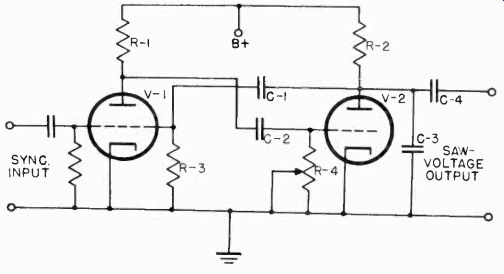
Figure 96. Multi-vibration circuit.
This action continues until V2 reaches cutoff and current ceases to flow through it.
8. V2 remains cut off until C2, dischargingthroughR4, produces a voltage drop, sufficient to permit V2 to conduct.
9. When no current was flowing through V2, there was no drop across R2 and the plate of V2 was at the full B supply potential.
Now, with current flowing, a drop occurs across R2, which reduces V2's plate potential.
10. This reduction is transferred through C1 to the grid of V1, where it produces a negative potential.
11. The negative potential reduces the current through V1, the drop across R1 decreases, and the potential at the plate of V1 increases.
12. Coupled to V2 through C2, the increase in potential on the plate of V1 causes an increase in the voltage on the grid V2.
13. This results in an increase in the current through V2 and a decrease in its plate current. Steps 10, 11, and 12 are repeated. This action continues until V1 is cut off, completing the cycle of operation.
The frequency of operation is determined by the values of resistance and capacitance employed.
3-59 The Cathode-Coupled Multivibrator. A special type of multivibrator, known as the cathode-coupled multivibrator or "Potter" circuit (after its originator) is used in many television receivers which have electrostatically deflected picture tubes. A cathode-coupled multivibrator circuit is shown in Figure 97. The basic difference between this circuit and that of Figure 96 is in the feedback circuit. In addition to the feedback condenser C2, coupling between the two stages takes place through the common cathode resistor Rc.

Figure 97. Cathode-coupled multi-vibration circuit.
The sequence of operation of the cathode-coupled multivibrator is as follows:
1. When the B+ voltage is applied to the plate of V2, capacitor C2 charges through R3 and R2. The B+ voltage is also applied to the plate of V1.
2. Plate current flows through V1 and V2, building up a bias voltage across the common cathode resistor Rc. The flow of plate current in V2 also lowers the plate-to-cathode resistance.
3. The bias voltage built up across Rc reduces the amount of current flowing in V1 and V2.
4. C2 discharges through R2 because of the lowered resistance path of V2.
5. The current flow through R2 places a high negative charge on the grid of V1, driving it to plate current cutoff.
6. As C2 continues to discharge through R2, the grid of V1 becomes less negative. V1 again starts to conduct.
7. When V1 conducts alter the grid bias is reduced from cutoff, the sudden flow of current produces a large positive voltage across Rc.
8. The voltage across Rc, which is common to the cathode of V2, drives the grid of V2 negative with respect to its cathode.
9. Less current flows in V2 as a result of the higher negative grid bias. The plate-to-cathode voltage drop is reduced and the plate voltage of V2 rises.
10. The higher plate voltage causes C2 to charge, thereby applying a positive voltage to the grid of V1 . This positive voltage increases the flow of plate current through V1, reinforcing the current which began flowing in step 6.
11. The increased bias voltage across Rc, as a result of this increased flow of current, is finally able to stop the flow of plate current through V2.
12. C2 has been charging until V2 stops conducting.
13. With V2 cut off, the current through Rc decreases and the negative bias voltage on the grid of V2 is reduced.
14. As V2 starts to conduct, C2 discharges through V2, R2, and Rc.
15. The current flowing in R2 builds up a negative voltage on the grid of V1, driving it to cutoff.
16. The grid of V1 is now in the same condition as during step 5, and the cycle begins again.
The variable resistor R2 controls the frequency of oscillation of the cathode-coupled multivibrator. It serves as the "hold" control in the sweep circuit.
3-60 Synchronizing the Multivibrator. If a sync signal is fed to one of the grids of the multivibrator circuit shown in Figure 96, and if the frequency of the sync signal is close to the natural oscillating frequency of the multivibrator, the sync signal will control the operating frequency of the multivibrator. A signal consisting of either positive or negative pulses may be injected into either of the grids to obtain synchronization. R4 is variable to permit adjustment of the natural oscillating frequency of the multivibrator.
The cathode-coupled multivibrator of Figure 97 is synchronized by applying negative sync pulses to the grid of V2. The discharge action of a cathode-coupled multivibrator begins with a negative pulse, developed on the grid V2 as a result of feedback voltage across the cathode resistor Rc. Therefore, a negative sync pulse, applied to this grid, will take over the triggering action and controls the frequency of oscillation.
3-61 Noise Effects. In a conventional synchronizing system, each individual synchronizing pulse triggers the blocking oscillator or multivibrator. The manner in which these circuits lock to the frequency of the sync pulses has already been described.
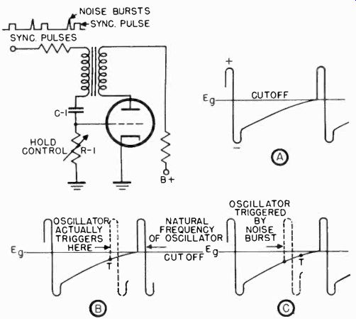
Figure 98. How noise affects the operation of blocking oscillator circuit.
Noise adversely affects the operation of conventional sync circuits. If noise of sufficient amplitude occurs close to the natural frequency of a blocking oscillator, it can trigger the oscillator as shown in Figure 98C. In Figure 98B, T is the time when the sync pulse occurs which triggers the oscillator before the end of its natural period. If a noise pulse occurs just before the sync pulse, as shown in Figure 98C, the noise pulse will trigger the oscillator. As a result, loss of synchronization takes place and the picture on the screen is distorted.
The effect of noise bursts on the stability of synchronization of receiver circuits emphasized the need for changes in the design of sync circuits, the shortcomings of "triggered" sync having become evident under operating conditions. Vertical sync circuits are considerably more immune to noise disturbances than are horizontal sync circuits. Under most conditions, ordinary vertical sync circuits are satisfactory. In areas where the signal-to-noise level is low, or where auto ignition and similar noise is prevalent, simple horizontal sync systems do not perform sufficiently well.
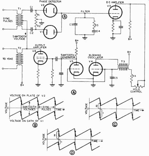
Figure 99. A.F.C. sync circuit and operating waveform.
In order to reduce the effects of noise on horizontal synchronization, a system which provides automatic frequency control of the synchronizing circuits has been developed. The addition of "AFC" results in a significant increase in noise immunity over that of receivers using conventional synchronizing circuits.
When it is used, random noise from diathermy, car ignition, and home appliances does not cause tearing of the picture and horizontal resolution is improved.
3-62 AFC Sync Circuits. The shortcomings of a synchronization system in which each sync pulse triggers the oscillator are obvious, since the oscillator cannot distinguish between a sync pulse and a noise pulse. In AFC sync circuits, a d-c control voltage is used, rather than individual sync pulses, to control the frequency of the sweep oscillator.
Figure 99A is a simplified diagram of one type of AFC sync system. As with conventional sync circuits, the sync signal is first clipped from the composite video signal and segregated into vertical and horizontal sync pulses. Instead of feeding the horizontal sync signals directly to the grid of the sync oscillator, they are injected into a phase detector, which compares the relative phase of the incoming sync pulses with that of the saw-tooth voltage in the output of the deflection circuit. If the sync pulses and the saw-tooth voltages are out of phase, the phase detector produces a signal which pulls the sync oscillator to the correct frequency.
The phase detector consists of two diodes, V1 and V2. The sync pulses are applied to the plate of V2 and the cathode of V1 through transformer T1. The saw-tooth voltage, tapped from the output transformer of the deflection amplifier is coupled to the phase detector at the center tap of the secondary of T1.
Since the saw-tooth voltage is fed into the secondary of T1, it has the same polarity on the plate of V2 as it has on the cathode of V1. The unidirectional sync pulses, on the other hand, are fed into the primary of T1 and appear 180 deg out of phase on the plate and cathode. When a positive sync pulse is applied to the plate of V2, the plate voltage is raised above ground by a voltage equal to the amplitude of the pulse. Simultaneously, a negative sync pulse is applied to the cathode of V1, which lowers the cathode voltage by an amount equal to the sync pulse amplitude. Figure 99B shows the signals on the plate of V2 and the cathode of V1.
Point A in Figure 99A is at the average of the potentials on the plate of V2 and the cathode of V1. In Figure 98B, this potential is zero because the saw-tooth voltage on the plate and cathode are of the same amplitude, above and below the zero voltage axis, at the time that the sync pulses occur. However, if a small phase displacement occurs between the sync pulses and the saw-tooth signals, as shown in Figures 99C and 99D, the average potential of the saw-tooth voltages is no longer zero.
If the saw-tooth shifts to the left, the average potential at point A becomes negative. If it shifts to the right, point A becomes positive. The changing voltage at point A is applied to the grid of V4 through an amplifier V3. The oscillator V4 can be either a blocking oscillator or a multivibrator. In the circuit shown, V4 is a blocking oscillator. This oscillator differs slightly from the circuit described previously. In this circuit, d-c voltage, determined by the setting of R4 (the hold control), is applied to the grid. This d-c voltage determines the point at which the oscillator will trigger. If the d-c voltage is raised, the oscillator will trigger sooner; if it is reduced, the oscillator will trigger later. Thus the frequency of the oscillator is controlled by the d-c voltage on its grid. The voltage is the potential at point A after it has been amplified by d-c amplifier V3. V3 is d-c coupled so as not to lose the d-c component at point A, which is necessary to the operation of the circuit.
If the sync pulses and the saw-tooth voltages are in phase, the potential at point A is zero and the scanning oscillator operates at the proper frequency. Should the scanning oscillator suddenly change frequency, the saw-tooth will shift in phase with respect to the incoming sync pulses, and the potential at point A will no longer be zero. The resultant voltage at point A is amplified and applied to the grid of the scanning oscillator to bring it back to the correct frequency. Thus, the frequency of the scanning oscillator is controlled by a d-c potential, rather than recurring sync pulses.
If a noise pulse is fed into the circuit of 99A, it will cause a rapid change in the d-c control signals at point A. The values of R3, C4, and C3 are chosen so that sudden changes are filtered to ground. In other words, only the regularly recurring sync pulses can determine the d-c control voltage, while random noise pulses have little effect. This system is sometimes called flywheel synchronization because of the "flywheel" action of the sync pulses in determining the average d-c control voltage despite sudden variations in the incoming signal.
Another type of AFC circuit is shown in Figure 100. This circuit eliminates the need for a manual hold control. A hold control is normally necessary to permit correction of frequency drift in blocking oscillators and multivibrators, the two types of sweep oscillators most common in television receivers. By using a more stable oscillator, the automatic characteristics of the flywheel system just described, can be greatly improved.
The horizontal oscillator used in the circuit of Figure 100 is a stable Hartley oscillator, operating at the horizontal sweep frequency of 15,750 cycles per second. Coil L1 is the oscillator coil. This coil is coupled to winding L2 and thus feeds a sine wave voltage to V1.
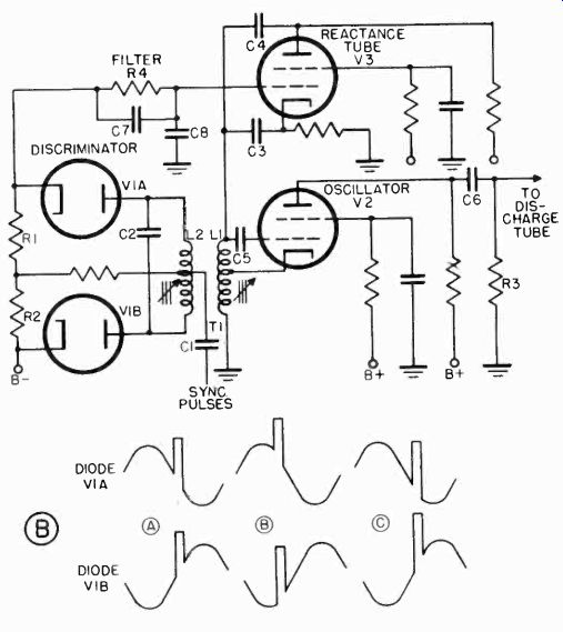
Figure 100. Automatic frequency control circuit which eliminates need for
manual hold control.
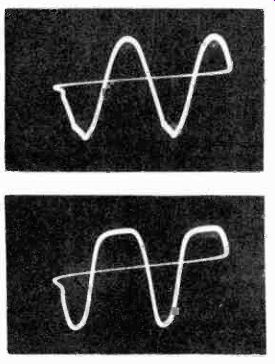
Figure 101. Signals on grid and plate of Hartley oscillator operating at
low plate voltage.