Circuit variations: Design Mechanical features
7-1 The fundamentals of television receiver circuit design were discussed in Section 3. Practically all of the circuits encountered in commercial receivers were covered in that section. If the reader thoroughly understands those basic circuits, he should have very little trouble in comprehending the operation of complete receivers.
In this section the mechanical and electrical design of typical television receivers is discussed. The first part of the section is devoted to descriptions of commercial RF tuning systems.
The latter portion of the section is devoted to descriptions of complete commercial receivers.
R-F tuning systems are treated separately because of their nature. A practical RF tuner is the result of careful mechanical and electrical design. The mechanical problems involved in the design of television RF tuners are difficult to solve. As a result, it has been necessary to resort to mechanical arrangements considerably more complex than those ordinarily encountered in electronic equipment.
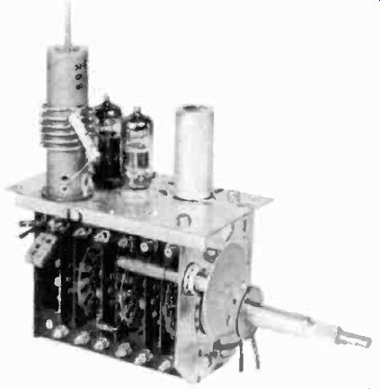
Figure 1. The RCA tuner. (courtesy RCA)
Numerous ingenious solutions to RF tuner problems have been found by the various manufacturers, as the reader will realize while reading this section. Most of the tuners described here will be found in more than one receiver model. As a rule, a manufacturer makes one tuner which he uses in all of his receiver models. Some tuners are actually used by several manufacturers since it has been the practice of a few firms to sell tuners and tuner components of their design and manufacture to other companies. In some instances this practice has been extended to complete receiver chassis.
The RF tuner section of a television receiver usually consists of the local oscillator, mixer, and RF amplifier stages.
Some receivers are not equipped with an RF stage, in which case the tuner consists of a mixer and a local oscillator. Most tuners are mounted on a separate chassis assembly which is, in turn, mounted on the main receiver chassis. This type of unitized construction makes it possible to pre-align the tuner section and then incorporate it into any one of a number of receivers.
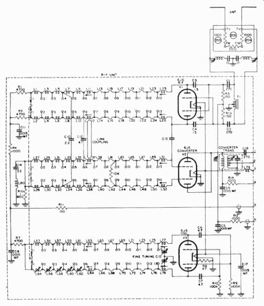
Figure 2. Schematic diagram of RCA tuner.
The most difficult problem in the design of an RF tuner is the broad frequency coverage required. At present, television stations operate on frequencies between 54 and 216 megacycles.
Two solutions have been found to this problem of frequency coverage. One solution makes use of a switching system which places different condenser, coil, or condenser and coil combinations in the tuner circuits for each television station. The reader will note that some of the tuners described provide switch positions for thirteen channels. These tuners were designed before the Federal Communications Commission modified the television allocations and excluded channel one. The second solution to the frequency coverage problem has been the use of continuously tuned, variable inductances. This type of design eliminates some of the contact problems which arise in switch type tuners.
7-2 The RCA Tuner. The RCA Tuner is mounted on a separate subchassis as shown in Figure 1. Located on this subchassis are the RF amplifier, converter, oscillator, fine tuning control, channel switch, converter transformer, RF converter, and oscillator coils, and all their tuning adjustments.
The unit provides for operation on all of the present television channels. It functions to select the desired picture and sound carriers, and amplifies and converts them to provide, at the converter plate, a picture IF carrier frequency of 25.75 Mhz and a sound IF carrier of 21.25 Mhz. As can be seen in Figure 1, this is a switching type tuner. The desired television channel is selected by means of a ganged switch which changes the inductances in the RF amplifier, mixer, and oscillator circuits.
Figure 2 shows a schematic diagram of the tuner. T1 is a center-tapped coil which short circuits undesirable low frequency signals picked up by the antenna before they can be applied to the control grids of the 6J6 RF amplifier, V1. C1 and C2 are antenna isolating capacitors. The d-c return for the grids of V1 is through R3 and R13 which also properly terminate the 300-ohm transmission line. C3 and C4 are neutralizing capacitors necessary to counteract the grid to plate capacitance of the triode RF amplifier in order to prevent oscillation.
In the plate circuit of the RF amplifier there is a series of inductances, L1 to L25 and L2 to L26 inclusive. These inductances act as a quarter wave section of a balanced transmission line which can be tuned over a band of frequencies by moving a shorting bar along its parallel conductors.
Coils L25 and L26 are adjusted to provide the correct length of line for channel 13 (210 216 Mhz). L13 to L25 and L14 to L24 are fixed sections of line which are added to L25 and L26 as the shorting bar is moved progressively down the line. Each one of these inductances consists of a small non-adjustable silver strap, mounted between the contacts of a switch, as shown in Figure 3. Each strap is cut to give a six-megacycle change in frequency. When changing from channel seven (174 180 Mhz) to channel six (82 88 Mhz), adjustable coils L11 and L12 are inserted. To provide for the remaining five channels, L1 to L9 and L2 to L10 are progressively switched in to add the necessary additional inductance. The switch is operated in continuous rotation and has no stop.
Coils L1 to L9 and L2 to L10 are unusual in that they are wound in figure eight fashion on fingers protruding from the switch wafer. This winding form produces a relatively noncritical coil because the coupling between turns is minimized.
A maximum amount of wire is used for the small inductance which is required, thus permitting greater accuracy in manufacture. These coils are visible in Figure 3 which shows the switch wafers.
The converter grid line operates in a manner similar to that of the RF amplifier. It is arranged on the switch so that coupling is provided between it and the RF line. C10, C12, C13, and a link, provide additional coupling which is arranged to produce a 4.5 Mhz band pass on all channels.
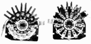
Figure 3. Water switches and coils used in RCA tuner. (courtesy RCA)
L80 and C14 form a series resonant circuit which is used to prevent IF feedback into the converter. The combination effectively grounds the grids of the converter at the IF frequency.
It also acts as a trap which rejects short-wave signals of IF frequency which arrive at the converter grids.
A 6j6 triode is used as a converter. The grids are fed in push pull by the incoming signal and the oscillator signal. The heterodyne products of these signals ( IF signals) appear in phase at the converter plates, which are connected in parallel. Unwanted signals of IF frequency which arrive at the converter grids in a push-pull manner appear at the converter plates out of phase. Since the plates are tied together, these signals cancel, thus reducing the possibility of interference.
The oscillator tuning line is similar to the converter and RF amplifier lines except that trimmer adjustments are provided for each channel and the low frequency coils are not figure eight windings. Brass screws are provided for adjusting channels seven through twelve. These screws are located close to tuning straps L66 to L76 (Figure 3). Brass cores are provided for adjusting coils L54 to L62.
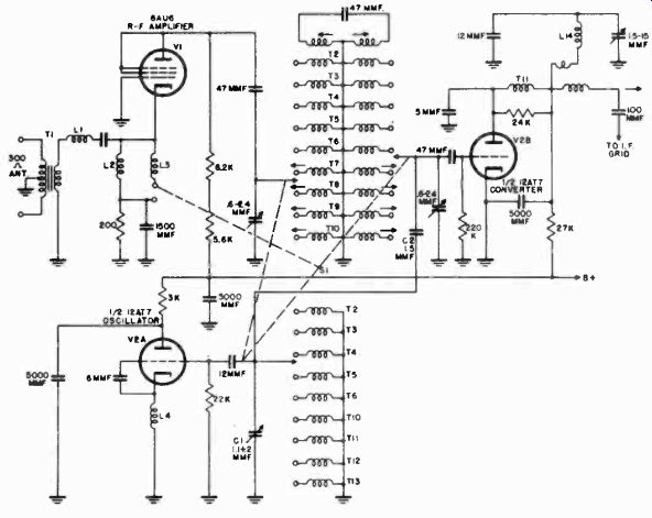
Figure 4. Schematic diagram of G.E. tuner.
C15 is a fine tuning adjustment which provides approximately 1600 khz variation of the oscillator frequency when tuned to channel one and approximately 3.8 Mhz on channel 13.
The physical location of the oscillator line with respect to the converter grid line is such as to provide coupling to the converter grids. This coupling is augmented by the link shown in the schematic. The combination provides a reasonably uniform oscillator voltage, at the converter grids, over the entire tuning range.
The converter transformer T2 is a combination picture IF transformer, sound trap, and sound IF transformer. The converter plate coil is assembled within the structure of a high Q resonant circuit tuned to the sound IF frequency.. This high Q coil absorbs the sound IF component from the primary. Thus the sound carrier is attenuated on the primary of T2, from which the first picture IF amplifier is fed. The sound IF appears on the secondary T2. The first sound 1-f amplifier is fed from a tap on this secondary.
7-3 The G-E Tuner. Like the RCA tuner, the G-E tuner is of the switching type. Provision is made for selecting any one of twelve channels by means of a ganged switch which inserts different combinations of coils and capacitors into the RF amplifier, oscillator, and converter circuits. An important difference between the RCA and G-E tuners is in the method used to obtain the necessary wide passband for each channel. In the RCA tuner, each channel is tuned by shorting out sections of a balanced transmission line. In the G-E tuner, individual coil and capacitor combinations are used for each of the twelve channels.
Figure 4 shows the circuit arrangement of the G-E tuner. Two tubes are used. A 6AU6 is used in the RF amplifier stage, while a dual triode, 12AT7, is employed as an oscillator and converter.
The 6AU6 is operated as a grounded-grid, RF amplifier. It is connected as a triode to reduce the noise generated in the stage.
The input circuit contains a balanced transformer T1, whose impedance is designed to match a 300-ohm transmission line.
The signal is coupled to the cathode of the amplifier. The cathode circuit is tuned to have a broad band characteristic. Only two coils, L2 and L3, are needed to broadly tune the cathode circuit over the low and high bands. The plate circuit of the RF amplifier contains double tuned, over coupled transformers which are switched in by the channel selector.
The oscillator V2A employs a modified Colpitts circuit. Separate coils are inserted into the circuit by a switch which is ganged to the RF switch. The oscillator voltage is capacitively coupled to the grid of the converter by a 1.5 mmf capacitor, C2, thereby eliminating the need for adjusting oscillator excitation.
A triode converter is used to hold the noise generated by the tuner unit to a minimum. Because it has a low equivalent noise resistance, the triode converter aids in improving the signal to noise ratio of the receiver. Both the RF signal and the oscillator voltage are capacitively coupled to the grid of the converter. The intermediate frequencies which result from the heterodyning of these two signals appear in the plate circuit.
The mechanical construction of the G-E tuner embodies several interesting features. For simplicity of design and to reduce cost, the tuned circuits of six of the higher channels are combined into three switch positions. This means that the band pass characteristics of the RF amplifier and converter in these three switch positions are sufficiently wide to pass two television channels. The oscillator trimmer, C1, has sufficient range under these conditions to cover both channels.
A ground plate is used in the band switch to connect the RF plate and converter grid coils to ground. This plate is so designed that it furnishes the coupling for the coils, making it unnecessary to adjust coupling. The coils used for the high channels have an unusual type of construction. They are self-supporting, being would with No. 20 Formex wire. The diameter and the pitch of the coils are made to conform to the threads of brass screws which are inserted into the coils. A wide range of tuning is obtained by adjusting the depth of the screw inside the coil. The adjustment is great enough to allow using the same type of coil for four different positions of the band switch, resulting in reduced manufacturing costs.
7-4 The Philco Tuner. This tuner consists of an RF amplifier, converter, and local oscillator. The desired channel is selected by means of a switching turret which inserts the proper set of coils into the amplifier, converter, and oscillator circuits.
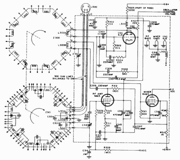
Figure 5. Schematic diagram of the Philco tuner.
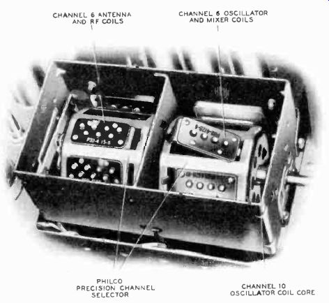
Figure 6. Octagonal turrets used in Philco tuner showing "snap-in" coils.
(courtesy Philco)
The antenna coil and the RF amplifier coil for each channel are built as an assembly. Eight separate coil assemblies are mounted on a drum type switching turret as shown in Figure 5.
The converter and oscillator coils for each channel are also built as assemblies and are mounted on a second switching turret.
This tuner provides for the reception of eight different channels. The reader will recall that twelve channels have been assigned for use by television stations. Since the FCC intends to assign a maximum of seven channels in any one area, the provision for only eight channels on the Philco tuner is not a disadvantage. Twelve sets of coils are available, any eight of which may be easily installed without soldering or wiring. These coils are built as "snap-in" assemblies which fit into the switching turrets (Figure 6). The turrets are octagonal in shape and each set of coils is mounted on a different face of the octagonal drums. The front drum carries the mixer and oscillator coils, while the rear drum holds the RF amplifier and antenna coils. The advantage of the turret construction is that the leads connecting the coils to the RF amplifier, oscillator, and converter states are short and of constant length for all channels. All the coils are mounted on the turret drum and each set is moved into position as required. Good contact between switch points is obtained by supporting the contact points with springs.
Provision has been made in the Philco tuner for the use of a high frequency antenna for stations operating in the frequency range between 54 and 88 Mhz, and another antenna for stations operating on frequencies between 174 and 216 Mhz. Separate input terminals are provided for each antenna, as shown in Figure 5. The antenna in use is determined by the position of the turret. This is accomplished by arranging the coils on the turret so that the RF and antenna coils for the low band channels occupy contact positions 1, 2, 4, 5, and 6; while the high band coils are connected to contacts 1, 2, 3, 5, and 7.
The signal from the antenna is coupled to the first RF stage through a small, center-tapped link, L301A. This link permits the use of a 300-ohm twin lead transmission line if the entire winding is employed. When a shielded coaxial transmission line is used in high noise areas, an impedance match can be made by connecting the shield of the cable to the chassis, and the center conductor to one of the two "LO" connections on J300 for the low band or to one of the "HI" connections for the high band. The impedance under these conditions is one fourth of the impedance of the whole winding a good match for 72-ohm coaxial cable.
The RF signals, both sound and picture, are fed to grid No. 1 of the 6AG5 RF amplifier, and are amplified in this circuit.
C311 permits grounding one end of L301C without shorting out the grid bias supplied by a.g.c. action. The 6AG5 RF amplifier is also biased through resistors R310 and R311 in series. R310 is not bypassed. This connection is made to prevent input capacity changes with variations in grid bias. If this method were not used to minimize these capacity changes caused by the "Miller Effect", they would change the response curve of the RF amplifier as the signal strength of the received station changed.
The coupling network used between the RF amplifier and the 6AG5 mixer consists of variable capacitor C310, coupling capacitor C309, series inductance L300B, and the input capacity to the 6AG5 mixer. In effect, the circuit is shunted by the 1800 ohm plate resistor, R312, of the 6AG5 RF amplifier. This low value of plate resistance is necessary to secure a flat response.
The screen of the RF amplifier is bypassed to ground by parallel capacitors C316 and C320. The 10 mmf capacitor C320 is most effective at the high frequencies, while the 470 mmf condenser C316 is most effective at lower frequencies. The output of the local oscillator is coupled inductively to the mixer through L300B and L300A of transformer Z300. An ultraudion is used as a local oscillator because it performs well at high frequencies. The tuned circuit is connected between the grid and the plate to produce the phase shift necessary for oscillation. The grid end of the tuned circuit is bypassed to ground through capacitor C304 to control the grid excitation. Grid-current flow through grid resistor R303, during oscillation, furnishes grid bias for the tube.
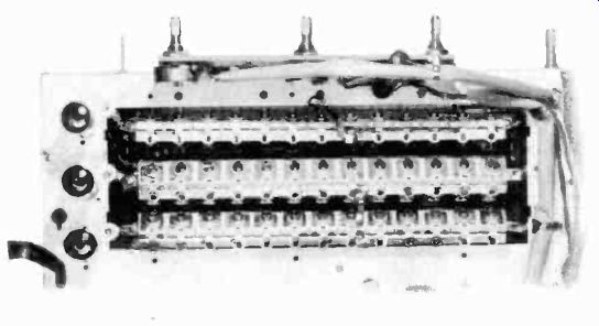
Figure 7. Layout of Hallicrafters thirteen channel, pushbutton tuner. (courtesy
Hallicrafters)
Fine tuning of the oscillator is obtained by the use of an oscillator control reactance tube (half of a 6J6 which is the second triode of the oscillator tube), controlled by the output voltage from the FM discriminator which is located in the Audio Section of the receiver. Drift in local oscillator frequency is corrected by the reactance tube, so that a constant IF output is produced. R-F voltage is fed from the local oscillator to the grid of the reactance tube through a network consisting of capacitor C305 and resistor R306 in series. Phase shift of the voltage applied to the grid of the reactance tube is obtained by the combination of C305 and R306. Because of the phase shift in the voltage applied to the grid, the reactance tube draws a current that is out of phase with the voltage appearing across the oscillator coil. The reactance tube draws a leading current, and it therefore acts as a capacitor whose value is determined by the current flowing in the reactance tube. As the grid bias varies the current, it also varies the frequency of the local oscillator. This grid bias is the d-c voltage fed back to the reactance tube from the discriminator. When the sound intermediate frequency is centered about the correct frequency, the d-c voltage at the center point of the discriminator is zero. If the center frequency drifts above or below the correct value, the output voltage will be a positive or negative d-c potential, respectively. This varying potential is applied to the grid of the reactance tube. The net effect of this feedback voltage is to force the oscillator back to its correct frequency.
7-5 The Hallicrafters Tuner. The Hallicrafters tuner is an example of a pushbutton switching tuner. The pushbutton switch assembly is shown mounted on the front of the receiver chassis in Figure 7. When the desired button is depressed, appropriate capacitors are switched into the RF amplifier and oscillator circuits.
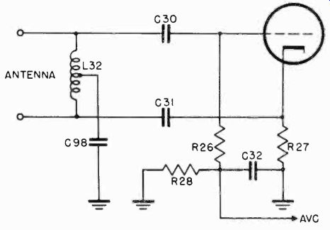
Figure 8. Antenna input circuit.
The tuner consists of three stages, an RF amplifier, a mixer, and a local oscillator. The input to the RF amplifier is designed to match a 300-ohm transmission line. A balanced 300-ohm load to the transmission line is obtained through the use of a combination of grid and cathode input to the RF amplifier. This circuit arrangement is shown in Figure 8. L32 is a balancing coil.
Its center tap is grounded to RF by C98. A direct ground to the chassis cannot be used at this point because in the Hallicrafters receiver one side of the a-c power line is connected to the chassis. A direct connection at this point would constitute a shock hazard. C30 and C31 perform the same function as C98 in reducing shock hazard, and in addition function as d-c blocking capacitors. R26 and R27 are each 150 ohms, and since R27 is directly grounded and R26 is grounded to RF through C32, they place a 300-ohm load, balanced to ground across the antenna.
One end of this balanced input is fed to the grid of the RF amplifier, the other end to the cathode. Since a signal applied to the grid of a tube has the same effect as a similar signal 180° out of phase applied to the cathode, the push-pull signals from the antenna reinforce one another in the input to the RF amplifier.
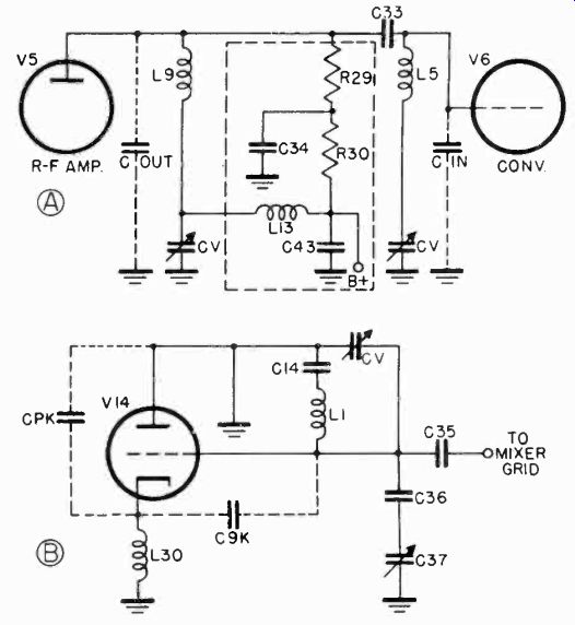
Figure 9. A. R-F amplifier circuit. B. Oscillator circuit.
The tuned circuits employed in this tuner are illustrated in Figures 9A and 9B. Figure 9A shows the tuning of the plate of the RF amplifier and the grid of the mixer. R31 (the converter grid return) and some inductors, capacitors, and resistors have been eliminated for the sake of simplicity. If the components enclosed in the dashed lines are temporarily ignored, it will be observed that the circuits on either side of C33 are the same. Cout is the output capacitance of the RF amplifier which is resonated with the coil L9 to provide the broadband characteristic required to pass the RF frequencies. Cin is the input capacitance of the mixer. It also forms a broad band resonant circuit. The variable capacitors Cv are those selected by the pushbutton switches to tune each channel. L13 and C43 decouple the B from the plate circuit. R30 and C34 perform the same function for decoupling the screen which is connected to their junction.
A.V.C. voltage is applied to the RF amplifier at the low end of grid resistor R29. This effectively places the A.V.C. voltage in series with the RF grid voltage.

Figure 10. The Inductuner. (courtesy DuMont)
The oscillator, which is shown in Figure 9B, utilizes a modified Colpitts circuit. The diagram has been drawn in such away as to emphasize the Colpitts type of circuit. The d-c grid and plate connections have been omitted for simplicity. Cpk is the plate-cathode capacitance and Cgk is the grid-cathode capacitance. The variable capacitor Cv, which is part of the tank, represents the tuning capacitor chosen by the push-button switch assembly for the channel in use. C36 is a fixed capacitor in series with C37, which is the fine tuning control. As is customary in television receivers, the oscillator is tuned to a frequency higher than the incoming signal. The oscillator voltage is capacitively coupled through C35 to the grid of the mixer, V6.
There are 39 tuning capacitors in the tuner. Each channel requires the substitution of three tuned circuits for the RF amplifier. the mixer, and the oscillator. Since there are 13 channels, a total of 39 capacitors are needed. Only one set of three capacitors is in use at one time so that the alignment of each channel is independent of the others.
7-6 The Du Mont R-F Inputuner. The Du Mont Inputuner is of the continuously tuned, inductive type, and differs considerably from the switch and turret type tuners previously described. The heart of the Inputuner is a three section variable inductance. This three section variable inductance is manufactured by P.R. Mallory and Company. It is known as the Inductuner.
Figure 10 shows the internal construction of the Inductuner.
It consists of three coils mounted on a ceramic shaft. At the right end of the shaft is an accumulation stop to prevent damaging the device if the shaft is turned too far in either direction.
Each coil is continuously tuned for 10 turns, resulting in an inductive range of 0.02 to 1.0 microhenries. A trolley contact moves along each coil, dividing it into used and unused sections.
The movable contact is shorted to the low frequency end of the coil so that the unused section is resonant at a very high frequency which lies outside of the desired tuning range.
The RF tuned circuit consists of a closely coupled pair of these variable inductors. These inductors are capacitively and inductively coupled and have a 4.5 Mhz bandwidth between double peaks of the response curve, and a 6 Mhz overall bandwidth.
This double tuned circuit covers, continuously, a range of 44 to 216 Mhz, while the third tuned circuit of the Inductuner covers the same range but is 21.9 Mhz higher in frequency, and is used for the local oscillator tuning circuit. These circuits are shown in the block diagram of Figure 11 and the schematic diagram of Figure 12.
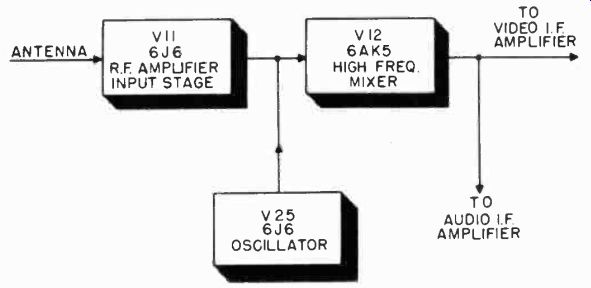
Figure 11. Block diagram of DuMont Inputuner.
The input tube is a cathode-driven, grounded-grid, double triode 6J6 which functions as a constant impedance, 72-ohm unbalanced input to match the 72-ohm coaxial transmission line.
Plate voltage is supplied through 10,000-ohm resistor R57 and decoupled by a 470 mmf capacitor C52. The RF signal resonant circuits are damped by a pair of 12,000-ohm resistors, R58 and R59. Both the 6J6 input tube V1l and 6AK5 mixer V12 are isolated from d-c by a pair of 15 mmf capacitors, C47 and C51.
V11 also acts as an RF amplifier working into the RF signal resonant circuits.
The 6AK5 high gain pentode V12, used as the mixer, has both the RF signal and the oscillator signal (at 21.9 Mhz higher than the RF signal) impressed on its control grid. The output of the mixer tube consists of a wide band of frequencies which include both the video and sound intermediate frequencies which are 4.5 Mhz apart.

Figure 12. Schematic diagram of Inputuner.
The oscillator uses one half of a 6J6 triode V25 in a modified Colpitts circuit. It is coupled to the mixer grid by a one mmf capacitor, C55. A capacity trimmer, C53, and an inductive padder are used for tracking purposes. 10,000 ohm resistor, R63, isolates the oscillator from the B+ line.
The Inputuner circuits are built up on a complete assembly and are pre-adjusted and pre-calibrated, after which the entire assembly is installed in the receiver. Figure 13 shows the complete Inputuner assembly with tuning dial.
7-7 Complete Receivers. The remainder of this section is devoted to descriptions of commercial receivers which are typical of the various models now on the market. The first receiver described is the Hallicrafters Model T-54 which is a typical seven-inch, electrostatic tube receiver. There then follows a description of the Philco Model 48-1000which contains a magnetic, 10 inch picture tube. This set is an example of the next price range of receivers. The Scott Model 13-A, employing the next size larger tube, the 12JP4, is then presented, followed by the Du Mont Model RA-101, which is operated with either a 15 inch or a 20 inch tube. Finally, the RCA Model 648 PTK is described to show the variations in circuit design which are required to produce a large screen, projected image.
In studying these circuits, the reader will become aware of the similarities as well as the differences between commercial designs. For example, the flywheel synchronization circuit for the horizontal sweep system is used by many manufacturers.
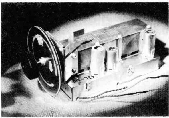
Figure 13. Complete Inputuner assembly for continuous 44-216 Mhz coverage,
showing manual drive dial. (courtesy DuMont)
The Scott, DuMont, and RCA receivers described in this section employ this circuit. Similar versions of the kickback circuit for obtaining the high voltage for the picture tube will be found in the Philco, Scott, and RCA designs. On the other hand, differences will be noted in the types of tuning mechanisms, IF amplifiers, sync circuits, and deflection circuits which are used by different manufacturers.
In order to avoid repeating detailed descriptions of circuits which are familiar to the reader at this point in the text, only those features not found in receivers already described are treated in detail.
7-8 The Hallicrafters Model T-54. The Hallicrafters Model T-54 is a table model television receiver with an electrostatic type 7JP4 picture tube. A picture approximately 5-3/8 inches wide by 4-3/8 inches high is obtained on the seven inch tube.
One of the unique features of the Model T-54 is its use of the intercarrier sound system which employs a single group of IF amplifiers for both the video and audio signals. Another distinguishing feature of this receiver is its transformerless, low voltage power supply. A selenium rectifier, operated in a voltage tripler circuit, eliminates the need for the transformer.
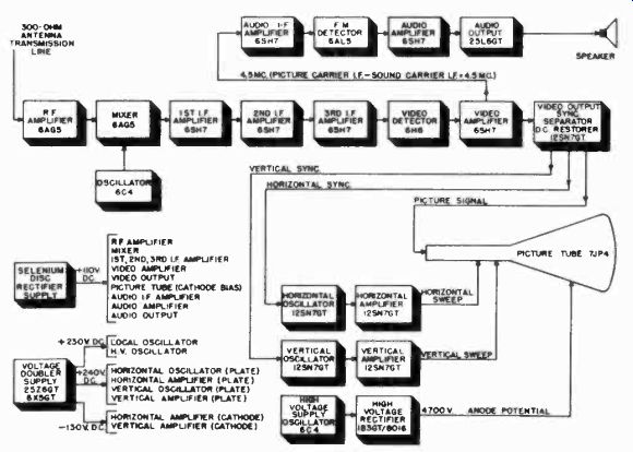
Figure 14. Block diagram of Hallicrafters Model T-54.
For ease of understanding, a block diagram is given in Figure 14. A more detailed schematic circuit is presented in Figure 15.
The Model T-54 employs the Hallicrafters 13 channel, pushbutton tuner described previously. This tuner may be seen in the view of the chassis shown in Figure 7. It will be noted that the entire receiver is built up on this single chassis.
7-9 Video Section. Included in the video section are the video IF amplifiers, the video detector, and two video amplifiers.
Contrary to usual practice, a single channel is used in this receiver to amplify both the video and sound IF signals. (In addition, there is a single stage of audio IF amplification which is discussed later.) Ordinarily, separate IF amplifiers are used for video and sound to prevent interaction between the two signals. In this receiver, this interaction is put to use. The two carriers beat together in the video detector, giving a 4.5 Mhz signal. This signal may be considered as a second (sound) IF.
It is frequency modulated just as the first sound IF, and may be demodulated by conventional techniques. This type of sound system is referred to as the intercarrier sound system.
There are three stages of IF amplification, V7, V8, and V9, and four associated tuned circuits. A combination of broadband tuning and stagger tuning is employed to obtain an amplifier response sufficiently broad to cover the video and audio carriers.
Each tuned circuit is peaked to a separate frequency as follows: L14-25 Mhz, L15-22.5 Mhz, L16-24.5 Mhz, and L17-23.3 Mhz. In addition, each circuit is loaded by a resistor to broaden the response of each stage. For example, L14, the plate load of the mixer V6, is a variable inductor having a movable core. It is tuned by the output capacitance of the mixer and the input capacitance of the following stage, V7, the first IF amplifier.
In order to lower the Q of the tuned circuit in the interest of attaining a broad pass band, it is loaded by the 27,000-ohm grid resistor R33 of the following stage. L15, the plate load of the first IF amplifier, and L16, the plate load of the second IF amplifier, are tuned and loaded in the same manner. L24, the plate load of the third IF amplifier is simply an untuned coil.
However, the signal from this plate is fed to the cathode of the diode detector, and in this cathode there is a variable inductor, L17, which tunes the coupling circuit for broadband response.
This inductor is of the same design as L14, L15, and L16. It is loaded by the input resistance of the diode. The band-pass characteristic obtained by the combination of stagger-tuning and broadband tuning is shown in Figure 16.
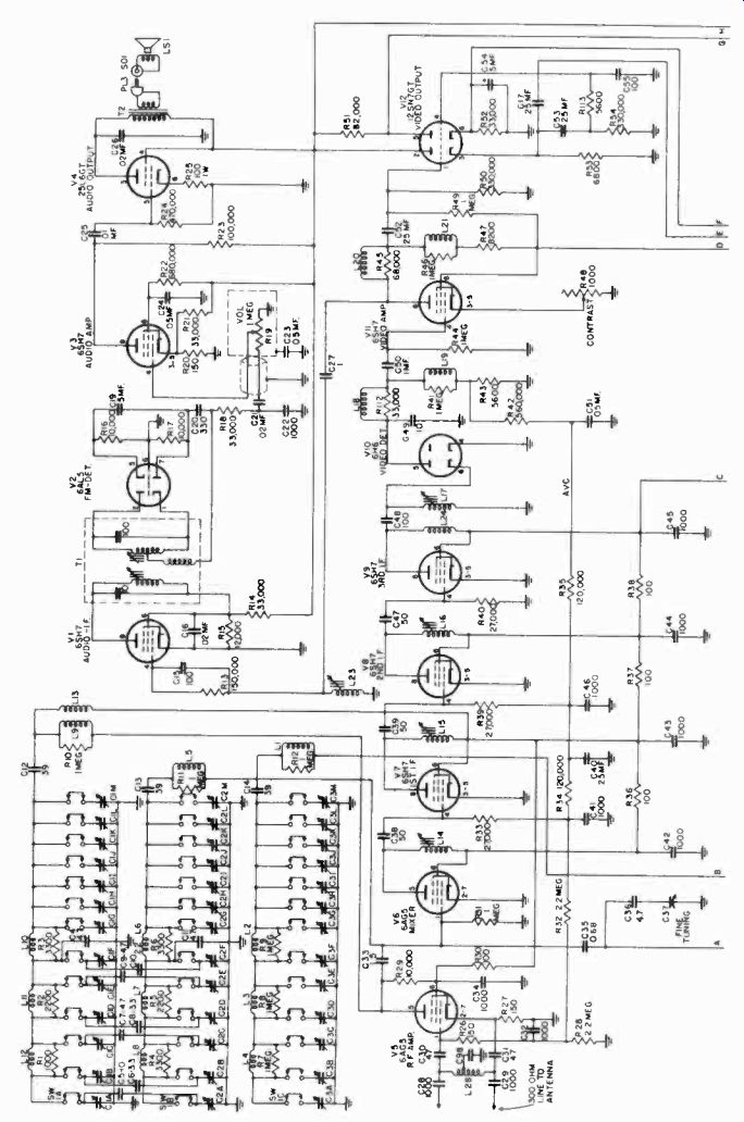
Figure 15.
It will be observed from this pass band characteristic that the response curve is sufficiently narrow to exclude adjacent channel interference without the need of traps. This is possible because with a seven inch picture tube adequate definition is obtained with a relatively narrow response curve in this case, the curve is flat for less than 2 Mhz. By narrowing the response curve, the 21.75 Mhz sound IF carrier is fairly well attenuated. Therefore, one 4.5 Mhz trap (C27 and L23) in the plate circuit of the video amplifier is sufficient to prevent the sound signals (which are located 4.5 Mhz away from the video carrier) from getting into the picture channel. C27 and L23 form this series resonant trap. At the resonant frequency of 4.5 Mhz, the impedance of this circuit is very low and the 4.5 Mhz signal is shunted through this trap and therefore is not passed on to the picture tube. The 4.5 Mhz sound signals, which have been by-passed by this trap from the video circuits, are fed to the grid of the 4.5 Mhz sound IF amplifier, V 1. On the other hand, since the sound IF carrier has been amplified along with the video IF carrier, the combination of the two produces a sufficiently strong beat signal, which, after a single stage of audio IF amplification, is strong enough to operate the ratio detector, V2.
A.V.C. voltages are applied to the first and second IF amplifiers, but not to the third.
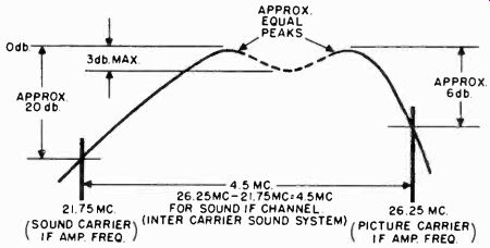
Figure 16. Response curve of intermediate frequency amplifiers which pass
both the video and audio signals.
7-10 Detector. A single diode V10 is used in a conventional rectifier circuit as the video detector. The polarity of the video signal is negative at the output of the detector. The d-c output appearing across R43 is filtered by capacitor C51 and applied to the first and second video IF amplifier as a.v.c. voltage.
7-11 Video Amplifier. The output of the detector is coupled through a high frequency compensating circuit, employing both shunt and series-peaking coils, to the grid of the first video amplifier V11. This stage employs a high transconductance pentode which gives a gain of 20 to 25. Variable resistor, R48, in the cathode circuit of this stage, serves as a contrast control.
It varies the bias on the grid, thereby controlling the gain of the stage.
The output of the first video amplifier is fed through a high frequency compensating circuit to the grid of the second video amplifier, half of V12. This amplifier is one section of a dual triode connected as a cathode follower. Its output is applied to the cathode of the picture tube and to the grid of the second section of the dual triode. (This second section functions as the d-c restorer and sync separator described later). The purpose of the cathode follower is to match the high impedance of the compensating network in the plate circuit of the first video amplifier to the low impedance of the picture tube cathode. The gain of the second video amplifier (cathode follower) is approximately 0.65 times.
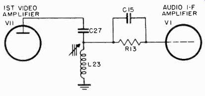
Figure 17. Coupling circuit for separating video and audio signals.
A second output from the first video amplifier is obtained directly from its plate, rather than through the compensating network. This is the 4.5 Mhz beat signal, which goes to the audio section. The method of coupling is illustrated in Figure 17. C27 and L23 are series tuned, so that they present a near short to the 4.5 Mhz beat at this point. This prevents the beat signal from continuing further to the picture tube where it would interfere with the video signal. Also, by virtue of the series tuning, a large 4.5 Mhz signal appears across the individual components of the series tuned circuit. The signal appearing across the inductor provides the input to the audio IF amplifier.
The first video amplifier has still a third function, as a noise limiter. Since the output of the detector is such that the sync pulses are negative, any high amplitude noise pulses riding on the sync signals will drive the grid of the first video amplifier very negative. This will cut the amplifier off and the noise will not pass through to the plate circuit. Elimination of these noise signals at this point helps to stabilize the sync circuits.
7-12 Sync Separator and D-C Restorer. Usually the d-c restorer is treated as part of the video amplifier, and the sync separator as part of the sweep system. However, in this receiver a single triode (the second half of V12) performs these two functions, and it is therefore logical to treat them together.
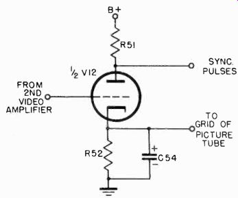
Figure 18. Sync separator and d-c restorer.
The circuit is shown in Figure 18. At the grid, the sync pulses are positive since the polarity of the output of the detector is reversed in the first video amplifier, but not in the second which is connected as a cathode follower. The cathode resistor and capacitor are very large; R52 is 33,000 ohms and C54 is 5 microfarads. This combination causes the stage to act very much like an infinite-impedance detector. The peaks of the sync pulses on the grid are just high enough to cause conduction through the tube; the charge developed on the cathode capacitor cannot leak off quickly through the large resistor R52, so that the tube is biased beyond cutoff except at the peak of each cycle of input. Since this bias corresponds to a value slightly below the peaks of the sync signals, it corresponds to the black level of the video signal. Therefore, if this bias voltage on the cathode is applied to the grid of the picture tube, it sets the d-c level in the video signal corresponding to black.
In addition to providing for d-c reinsertion, as described above, the same stage also separates the video signals from the sync pulses. Since the tube conducts only on the peaks of the input signal, the plate current flows in pulses, causing pulses of voltage to appear across the load resistor, R51. These are the sync pulses. However, because the tube is cut off at the video signal level, video signals do not come through. In this manner, the tube also acts as a sync separator. The sync pulses in the plate circuit are fed to the sweep multivibrators. The horizontal and vertical sweep circuits of this receiver are the same in all major respects, except, of course, there are certain differences in detail which stem from the difference in operating frequencies.
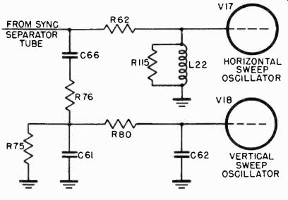
Figure 19. Networks for separating horizontal and vertical sync pulses.
7-13 Horizontal and Vertical Sync Separation. Since both the horizontal and vertical sync pulses appear in the output of the sync separator tube, some means must be provided to distinguish between them before they are applied to the sweep oscillators.
The networks which separate the two types of sync signals are shown in Figure 19. Pulses, fed through the d-c blocking capacitor, C66, to the lower integrating network, charge capacitors C61 and C62 through resistors R76 and R80. Between pulses the charge leaks off. When short duration horizontal pulses are applied to the network, the charge leaks off almost completely between pulses. The resultant voltage applied to the grid of the vertical oscillator is negligible. However, when a wide vertical pulse is applied, a voltage sufficient to trigger the vertical oscillator is built up across the capacitors. Part of the charge leaks off in the serration intervals, but they are so narrow that their effect on the operation of the network is very slight. Resistor R75 forms a voltage dividing network with R76.
This voltage divider produces a vertical sync signal of the proper amplitude to trigger the vertical oscillator.
The upper network shown in the figure is a conventional differentiating circuit. The horizontal, equalizing, and serrated vertical sync pulses are differentiated into sharp negative pulses occurring at the horizontal frequency. These are fed to the horizontal sweep oscillator to maintain synchronism. Resistor R115 performs the same function of reducing sync pulse amplitude as does R75 in the lower network.
7-14 Sweep Oscillators. The sweep oscillators are multivibrators. The vertical sweep amplitude is controlled by means of potentiometer, R84, connected across the output of the sweep oscillator V18. The vertical hold control, R82, adjusts the natural frequency of the oscillator so that it is triggered correctly by sync pulses applied to the grid from the integrating network.
Since the horizontal sweep oscillator, V17, runs at a much higher frequency than the vertical oscillator, a different method of sweep amplitude control is required. If the same method of connecting the width control across the output of the oscillator were used, the distributed capacitance in the potentiometer R114 in conjunction with its resistance, would distort the sweep waveform at the horizontal frequency of 15,750 cps. In this case, then, the sweep amplitude is controlled by varying the charging voltage available at capacitor, C69, across which the sweep saw-tooth voltage is generated.
7-15 Sweep Amplifiers. The output of the vertical sweep oscillator is fed through the height control, R84, to one section of a dual triode, V20, functioning as a conventional RC coupled amplifier. The entire output of this section is applied to one of the vertical deflection plates of the picture tube. In addition, part is tapped off and applied to the second section of the tube through C75 and a voltage divider, R88 and R91. The loss in the voltage divider is just equal to the gain in the first tube, so that the signal applied to the second section is the same as that applied to the grid of the first section, but of opposite polarity. The output of the second section is therefore 180° out of phase with the output of the first section. The sawtooth voltage from the second section is applied to the other vertical deflection plate of the picture tube. Balanced, push-pull deflection is thus obtained. A similar amplifier-phase inverter combination, V19, is used to deliver the horizontal sweep signal to the picture tube.
7-16 Picture Tube. The type 7JP4 picture tube is operated with its cathode approximately 200 volts above ground. This permits the necessary direct connection to the grid from the d-c restorer, since this d-c restorer operates from the common low-voltage power supply. With the cathode operated at a relatively low voltage, the picture tube heater can be connected to the heaters of the other tubes in the receiver. D-C voltage is applied to the cathode through variable resistor R56. R56 varies the cathode bias and serves as the brightness control.
7-17 Power Supplies. There are three major power supply sections, the heater supply, the low-voltage supply, and the high voltage supply.
Since this receiver has no power transformer to step the a-c voltage down to 6.3 volts for heater power, the heaters are connected in series in the same manner as in a-c, d-c sets. The voltage drop across the heaters adds up to the line voltage. Two diodes, V15 and V16, and a selenium rectifier, CR-1, are used in the low voltage supply. One of the tubes, V15, is a dual diode, the first section of which is used in a negative-voltage supply.
The cathodes of the sweep amplifiers are returned to this supply (the bottom of R74) rather than to ground, thus increasing their effective plate to cathode voltages. The negative supply delivers 125 volts.
The second section of dual diode V15 is used with diode V16 and a selenium rectifier in a positive voltage-tripling supply.
This supply is tapped at three points, giving 120, 230, and 390 volts. The 120 volts is developed across C60A which charges up through the selenium rectifier. L25 and C60B filter the rectified d-c voltage. This 120 volts is also applied to the plate of the V15 rectifier. When this tube conducts, it adds 120 volts to the 120 volt charge built up on condenser C58B. R72 and C58A filter the 240 volts across C58B. Because of the voltage drop in R72, about 230 volts d-c appear at the output of the filter across C58A. The 240 volts across C58B is applied to the plate of V16. When this rectifier conducts, this voltage is added to the voltage built up across condenser C57B. Thus, the tripled voltage, about 390 volts, appears across C57B. The high voltage supply is of the RF type. It incorporates a power oscillator, V21, operating at a frequency of approximately 200 khz. The oscillator is of the tuned-plate, tickler feedback type. The output voltage of rectifier V22 can be varied by changing the operating frequency of the oscillator by means of tuning capacitor C80. Plate power for the oscillator is supplied from the 230 volt tap on the low voltage power supply.
A supply of this kind has several advantages over one designed to operate directly from the a-c power line. The transformer T3 has an air core, making it light and compact. Also, the required filter capacitors, C81 and C82, are comparatively small, saving space and weight, and at the same time are less dangerous.
The danger is less because the small capacitors store less energy than larger capacitors operating at the same voltage. A shock from them is less likely to be lethal. Further, the regulation of such a supply is poorer than that of a 60-cycle supply, so that if accidental contact is made with it, the voltage will drop considerably because of the added load.
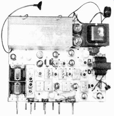
Figure 20. Chassis layout of Philco Model 48-1000. (courtesy Philco)
The high-voltage power supply is mounted on a sub-chassis, which is completely shielded. This reduces radiation and danger of accidental contact with the high-voltage circuit. Coup ling of the RF voltage to the other circuits is further reduced by RF chokes L26A and L26B in the low voltage leads.
7-18 Audio Section. The audio section is quite conventional.
As shown in Figures 15 and 19, the 4.5 Mhz intercarrier beat signal is fed from the plate of the first video amplifier to the grid of the audio IF amplifier V 1. Grid bias is developed by grid rectification of the signal, in conjunction with C 15 and R13.
The audio IF amplifier feeds a ratio detector V2, having a bandwidth of approximately 200 khz between peaks. The output of the ratio detector is fed through volume control R19 to the first a-f amplifier V3. The case of the volume control is grounded through capacitor C23 to minimize noise pickup. This control cannot be grounded directly because of shock hazard. The output of the first a-f amplifier, V3, is resistance coupled to the power amplifier, V4, a beam-power tube. The speaker is an oval, p-m dynamic.
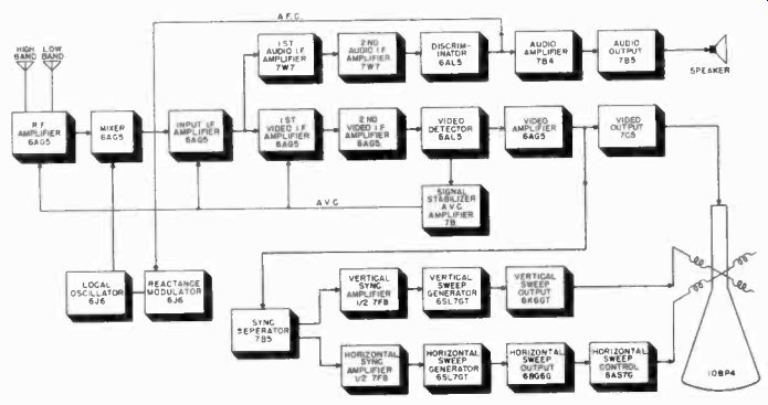
Figure 21. Block diagram of Philco Model 48-1000.
7-19 Philco Model 48-1000. The Philco Model 48-1000 is a ten inch, direct view, table model, television receiver. This model features a turret type of RF tuner which can select any combination of eight of the thirteen possible television channels. Provision is also made in the design of this tuner to use two antennas, one each for the low and high bands. Good stability is obtained through the use of an automatic frequency control circuit which prevents the oscillator from drifting off frequency. An a.v.c. circuit automatically controls the video and audio signal levels to maintain constant amplitude when the signal is fading.
The circuits are built up on one chassis, with the tuning unit enclosed in a separate sub-assembly (Figure 20). The cathode-ray tube and speaker are mounted in the cabinet and are connected via cables to the chassis.
A block diagram of the model 48-1000 is shown in Figure 21.
This receiver uses the Philco turret tuner described earlier in this section.
7-20 Video Section. The output from the tuner is fed to broadband input IF transformer, Z400, as shown in Figure 22. This transformer is a capacity-coupled type, with no inductive coupling between the primary and secondary windings. The amount of coupling is determined by the coupling capacitor C400B in series with C400A the more capacity used, the greater is the coupling. The use of decoupling networks consisting of R403 and C404 in the primary and R404 and C405 in the secondary, prevents interaction between stages. These networks, used throughout the receiver, may be recognized by the fact that they consist of a low-value resistor, feeding d-c voltage to plate, screen, and grid circuits, bypassed to ground at the point receiving voltage.
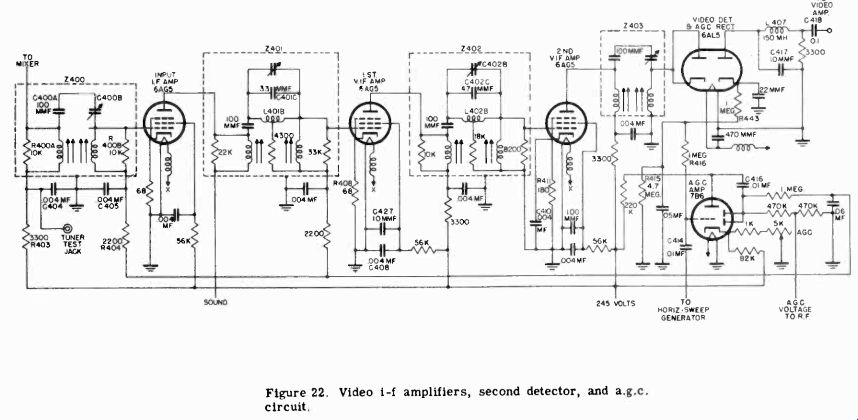
Fig. 22
The input IF transformer is of the over-coupled, broad-band type. The primary and secondary windings are tuned to the highest frequency of the band pass. The capacity of C400B is then increased, until an overcoupled double hump appears and spreads out to cover the desired band width. Both the primary and secondary windings are shunted by 10,000 ohm resistors, R400A and R400B, to broaden the band pass and to provide more nearly uniform frequency response. The output from Z400 is fed to the 6AG5 input IF amplifier.
The signal from the input IF amplifier is fed to IF transformer Z401. The design of this transformer is different from the one already described. A wave trap is inserted between the primary and secondary windings. By offering a high impedance to the sound IF frequency, this sound IF trap (C401C, and L401B) eliminates coupling between the primary and secondary, and prevents the accompanying sound from getting through. The trap is tuned to 22.1 Mhz, the sound IF carrier frequency. The sound IF signal is taken from a point preceding the sound trap, at the bottom end of the primary of the transformer, and is coupled to the input circuit of the sound section of the receiver.
The first video IF amplifier, a 6AG5, is biased by a combination of the a.g.c. voltage fed to its grid and the voltage developed across unbypassed, 68 ohm cathode resistor R408. The RF voltage appearing at the screen of the video IF amplifier is bypassed to ground by the combination of two capacitors, 0.004 mf capacitor C408 and 10 mmf capacitor C427.
The output of the first picture IF amplifier is coupled to the primary of transformer Z402. This transformer, which is similar to the input IF transformer Z401, consists of slug-tuned primary and secondary windings, with fixed capacity coupling and a parallel tuned trap circuit (C402B, C402C, and L402B). The trap circuit in this transformer is tuned to 28.1 Mhz. This trap is the adjacent channel sound trap.
A.G.C. voltage is not applied to the second video IF amplifier.
A 180 ohm resistor, R411, bypassed for RF by C410, is the only bias on the tube. The IF transformer Z403 is similar to Z400. 5 MP g33ì
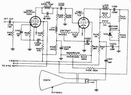
Figure 23. Video
amplifier.
The output from the plate of the second IF stage is fed to the last IF transformer Z403. No shunt resistors are necessary to broaden the response curve of this transformer because it is loaded by the 6AL5 diode detector. A 150 mh choke L407 and condenser C417 are used to filter the output of the second detector. Then the output is fed to the grid of the 6AG5 video amplifier. A 0.1 mf coupling condenser C418 feeds the signal to the first video amplifier.
7-21 A.G.C. Circuit. A.G.C. voltage is secured from the cathode of one of the diodes of the 6AL5 which acts as the second detector (Figure 22). This diode functions as an a.g.c. rectifier.
The rectified voltage developed across the network consisting of R443 and R415, at the cathode of the a.g.c. rectifier, is fed to the grid of the a.g.c. amplifier stage through resistor R416. A signal from the horizontal sweep generator is also fed to the grid of the a.g.c. amplifier through condenser C414. The signal at the plate of the amplifier is fed to the diode section of the 7B6 through condenser C416. Rectification takes place, and the voltage developed is filtered and fed to the grids of the tubes under a.g.c. control. The strength of the signal from the a.g.c. rectifier controls the amplification of the a.g.c. amplifier.
7-22 Video Amplifier. The 6AG5 video amplifier, shown in Figure 23, is designed to have as flat a response as possible.
The combination of 1,800 ohm resistor R428 and 40 mh inductance L411 provides the plate load of the amplifier. This type of plate load provides uniform output over a wide frequency range by maintaining a constant load impedance. The choke L411 increases the amplification at high frequencies, thus extending the frequency response of the amplifier to more than 4 Mhz. A 10 mf condenser is used to by-pass the low frequencies. The output of the video amplifier is fed through 0.05 mf capacitor C423 to the control grid of the 7C5 video output stage.
Output voltage is also developed across load resistor R426 in the screen of the video amplifier. This voltage is fed to the sync separator. The output from the plate is fed through a 4.5 Mhz trap, consisting of L408 and C421, to the grid of the 7C5 video-output stage. The sound carrier, beating with the picture carrier of the received signal, produces a beat frequency of 4.5 Mhz. If this beat frequency is not eliminated, it will produce a fine interference pattern in the picture. The purpose of the 4.5 Mhz trap is to prevent this beat pattern from appearing on the picture tube screen.
The plate load of the 7C5 consists of a network of resistors, inductors, and capacitors which are required to provide uniform frequency response. This plate load consists of 2,000 ohm resistor R436. A 70 mh peaking coil, L409, shunted by 27,000 ohm resistor R439, is used to compensate for the input capacity of the cathode ray tube and the stray capacities of the wiring.
7-23 Picture Tube. The d-c grid bias on the picture tube determines the average brightness of the picture. This average changes with the picture content, being one value for a picture composed mostly of blacks. The use of a d-c restorer establishes a voltage level which is independent of picture content, but which depends upon the sync pulses. This restorer consists of a crystal diode (1N34), shunted across a portion of the grid resistor of the cathode ray tube. The crystal conducts on the negative peaks of the video signal, developing on the cathode-ray tube a positive grid bias equal to the peak value of the negative sync pulses.
The desired brightness of the picture is controlled by control R433 which adjusts the cathode bias on the picture tube. The contrast of the picture is determined by the amount of video amplification and is controlled by contrast control R431.
7-24 Sweep Section. Positive sync pulses, both vertical and horizontal, are taken from the screen of the first video amplifier, and are fed to the grid of the 7B5 sync separator, shown in Figure 24. The sync separator tube has its cathode grounded, and the sync pulses charge condenser C500 through the tube.
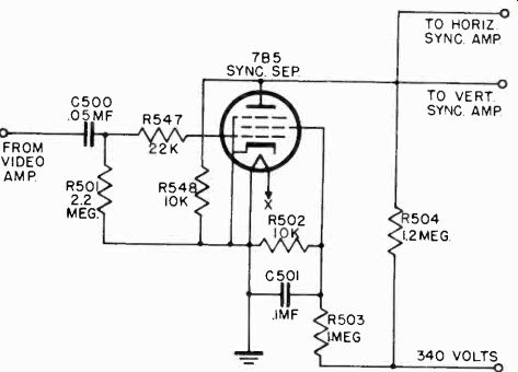
Figure 24. Sync separator.
The charge cannot leak off immediately, because of the long time constant of C500 and C501. Thus, the charge biases the tube at approximately cutoff. The charge on the condenser is almost equal to the peak amplitude of the positive sync pulses.
The picture portion of the signal has no effect on the plate current of the sync separator, as only the tips of the positive sync pulses can cause the tube to conduct. A 22,000 ohm resistor, R547, in the grid lead of the sync separator is used to prevent sharp noise pulses, such as ignition noise, from driving the grid highly positive and causing a blocking voltage to be developed.
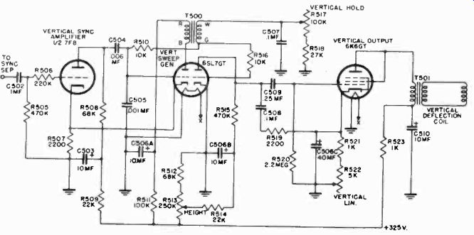
Figure 25. Vertical-deflection circuits.
Such a voltage would result in loss of sync for a portion of the picture. This resistor limits the amount of grid current that can flow for any one pulse. R504 and R548 form a voltage divider across the power supply, which places 2.6 volts on the plate of the tube. The voltage divider consisting of R503 and R502 places 3.2 volts on the screen grid. The very low plate voltage permits the sync pulses to drive the tube to saturation, clipping the sync pulses to uniform amplitude.
The negative output at the plate of the sync separator consists of vertical sync pulses and horizontal sync pulses. The pulses are fed to the inputs of the vertical sync amplifier. Both the vertical sync and horizontal sync pulses are applied as negative pulses to the grid of the vertical sync amplifier (half of a 7F8) but only the vertical pulses are effective. The vertical deflection circuits are shown in Figure 25. Being of very short duration compared to the vertical pulses, the horizontal pulses are not able to cause conduction in the vertical sync amplifier tube.
The negative vertical pulses cause a positive output pulse to be developed at the plate of the vertical sync amplifier. This signal is fed toC504 andC505, connected in series as an integrating circuit. At the output of the integrating circuit, a vertical sync pulse is obtained which is of sufficient amplitude to trigger the vertical sweep oscillator.
These pulses are applied to the grid of the vertical sweep generator. This oscillator is half of a 6SL7, operated in a conventional blocking oscillator circuit. The other half of the 6SL7 functions as a discharge tube to produce the vertical sawtooth voltage. The cathode of the discharge tube is at ground potential, and its grid is tied to the grid of the vertical blocking oscillator through R510. The discharge tube remains at cutoff until it is triggered. When the vertical oscillator fires, a sharp positive pulse is applied to the grid of the discharge tube. This pulse causes heavy plate current to flow and discharges the 0.1 mf charging condenser C508. R519 in series with C508 is a "peaking resistor" and adds the necessary negative pulse to the sawtooth voltage to create the waveform required by magnetic deflection circuits. The amount of sweep voltage is determined by the adjustment of the 250,000 ohm height control R513, which varies the d-c voltage at the plate of the discharge tube.
The sweep signal is coupled to the grid of the 6K6 vertical output stage through 0.25 mf capacitor C509. A 1,000 ohm cathode resistor R521 and a variable 5,000 ohm vertical linearity control, R522, are used to adjust the bias on the vertical output stage. This bias adjustment is used to maintain linearity of the output sawtooth voltage. The 6K6 is triode connected, and its output is fed to the vertical deflection transformer, the low impedance secondary of which is connected to the vertical deflection coil in the yoke. The vertical deflection coil is shunted by two 1,000 ohm resistors to damp out oscillations in the coils.
Vertical as well as horizontal positioning of the picture on the screen of the tube is accomplished by means of a movable magnetized ring which is built into the deflection yoke assembly.
The magnetized ring is moved in a horizontal plane to center the picture vertically, and in a vertical plane to center the picture horizontally.
The output of the sync separator is also applied to the grid of the horizontal sync amplifier shown in Figure 26. Since the cathode is grounded, this stage operates without grid bias, and the negative sync pulses on its grid cause a voltage rise across R527 and produce positive sync pulses at the plate. These sync pulses are coupled through the 0.001 mf capacitor C513 to the bottom end of the grid winding of the blocking oscillator transformer. The grid of the horizontal discharge tube is connected to the grid of the horizontal oscillator, and its grid is driven positive during the firing of the horizontal oscillator tube. This discharges the charging capacitor C516.
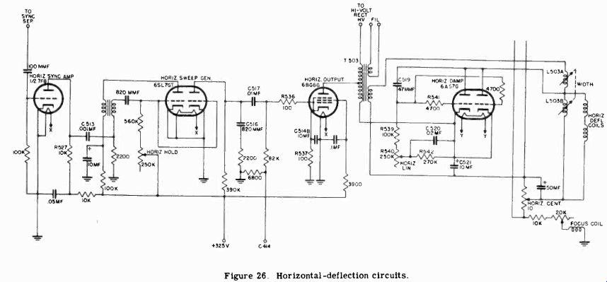
Fig. 26
The horizontal sawtooth voltage is coupled to the grid of the 6BG6 horizontal output stage through 0.01 mf capacitor C517 and 100 ohm resistor R536. The resistor is used to prevent oscillation in the horizontal output stage. Cathode bias for the 6BG6 is developed across cathode resistor, R537 bypassed by capacitor C514B. The sweep output is fed to a tap on the primary of the horizontal output transformer. One winding of this transformer is connected to the horizontal deflection yoke and the horizontal damping tube. The positive portion of the oscillations generated in the deflection coil during the rapid decay of the sawtooth signal is rectified by a 6AS7G horizontal damping tube and charges the condensers C519, C520, and C521. This voltage is applied to the horizontal output tube through transformer T503. The polarity of this charge is such that the voltage appearing at the plate of the horizontal output tube is equal to the B+ supply voltage, plus the charge across the condensers. This higher voltage results in greater sawtooth current through T503 and a greater deflection without an increase in the voltage of the power supply. The action of resistors R539, R540, R541, and R542, shunting the 6AS7G damping tube, together with C519, C520, C521, and L503 provides damping across the deflection yoke.
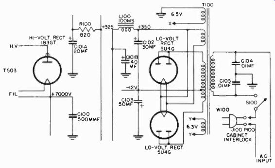
Figure 27. Power supplies.
7-25 Power Supplies. The low voltage power supply is a heavy duty type, designed to supply the relatively heavy currents required by a receiver with magnetic deflection circuits. See Figure 27. The primary circuit of the transformer is provided with an interlock to open the primary circuit when the cabinet back is opened. The primary is bypassed to ground by 0.01 mf capacitors C104 and C105. These capacitors help to eliminate noise pickup from the a-c line. Four secondary windings are provided. One supplies 6.5 volts for the filaments of all tubes, except the 5V4G, the high voltage rectifier and damper tube.
A 5 volt winding is provided for the two parallel connected rectifiers. A separate 6.3 volt winding supplies current for the 6AS7G damper tube filament. A high voltage winding supplies approximately 300 ma at 360 volts. The center tap of the high voltage winding is connected to ground through the 10BÁ4 ion trap coil, the focus coil, and focus control. This method of connection results in the development of about-12 volts.
The high voltage for the second anode of the picture tube is obtained by means of a high voltage winding on the horizontal output transformer T503. This high voltage winding steps up ...
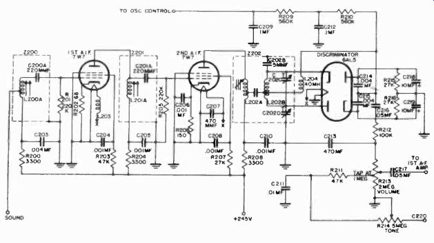
Figure 28. Sound IF amplifier and discriminator.
... the horizontal sweep voltage to approximately 7,000 volts. The reader will recognize this type of power supply as the kickback circuit. The high voltage is rectified by a 1B3GT rectifier tube and filtered with a 500 mmf ceramic capacitor C100. Adequate filtering is obtained with this small capacitor since the ripple frequency is 15,750 cps. The capacitance between the high voltage anode of the picture tube is added to the filter capacitance and further filters the high voltage supply.
The 1.25 volts for the filament of the 1B3GT heater is obtained by a single turn of wire on the horizontal sweep output transformer.
7-26 Sound Section. After the video IF signal and the sound IF signal are separated, the sound IF signal is fed to the input tap on Z200 in Figure 28. Z200 is an autotransformer, which steps up the voltage and applies it to the grid of the 7W7, first sound IF amplifier. A 220 mmf coupling capacitor C200A couples the voltage to the grid, and 220,000 ohm resistor R201 provides the d-c grid to ground path. The output from the plate is fed to second sound IF transformer Z201. This transformer which is similar to Z200, is capacity coupled to the grid of the second IF amplifier stage. The output from the second sound IF amplifier is fed to discriminator transformer Z202, operated in a ratio detector circuit.
The 6AL5 twin diode in the ratio detector is so connected that the output voltage to the audio amplifiers from the center tap of the two 0.004 mf condensers C214 and C215 is the algebraic sum of the voltage across each condenser. The peak output voltage of the two diodes is applied to two 10 mf capacitors connected in series (C218 and C219), with their center tap connected to ground. When a signal is received, the output of the two diodes charges the two 10 mf condensers to a voltage where amplitude depends upon the strength of the received signal. The center tap of the discriminator transformer secondary is connected through a 40 mh choke L204 to the midpoint of 0.004 mf capacitors C214 and C215. This center tap is connected to the midpoint to create a d-c charging path for the 0.004 mf condensers.
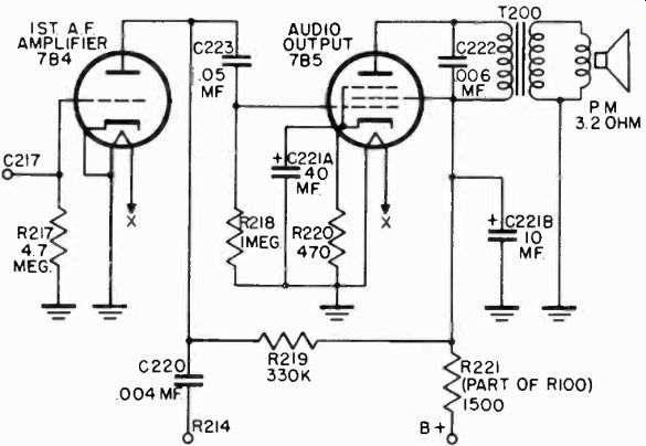
Figure 29. Audio amplifier.
With the signal at resonance, the voltage developed by one diode section is equal to that developed by the other diode section. Under these conditions, the voltage to the audio amplifiers, at the center tap of the 0.004 mf condensers, is zero. If the carrier frequency shifts higher, the voltage produced by one diode section is greater than that produced by the other diode section.
The total voltage across the two 0.004 mf condensers C214 and C215 will equal the d-c potential of the two 10 mf storage condensers. However, the output to the audio amplifiers will be the algebraic sum of the voltage across each of two condensers C214 and C215. This means that the maximum audio output from the discriminator is dependent upon the d-c voltage at the two 10 mf storage condensers C218 and C219. Sudden noise peaks will be lost in the charging of C218 and C219 because of their high capacity. Hence, no limiter stage is needed.
If a stronger station is tuned in, a greater charge is produced on the two series storage capacitors. This greater charge results in a greater audio variation. The mid-point of capacitors C214 and C215 will also assume a d-c potential to ground, varying as the received signal varies, higher or lower than the resonant frequency of the discriminator transformer. This d-c potential is filtered to remove the sound component. The filter consists of R210, C212,R209, and C209. It is then fed back, as control grid bias, to the grid of the reactance modulator which automatically controls the frequency of the local oscillator. A de-emphasis circuit consisting of R212 and C213 is connected from the discriminator output to the 2 meg. volume control R213.
The audio amplifier section of the receiver, as shown in Figure 29, is a conventional audio amplifier. The output of this amplifier and speaker while the Scott video receiver provides all the remaining circuits necessary for the reception of both television and FM programs. A 30 foot length of audio cable is provided to connect the video receiver to the Scott radio in order to utilize the high quality Scott audio system in the radio to reproduce the sound of the television and FM programs.
The video receiver consists of two chassis, the main receiver chassis and the power supply chassis. The low voltage power at 300 volts d-c and 400 volts d-c, as well as the high voltage 10 kv for the picture tube are located on the power supply chassis.
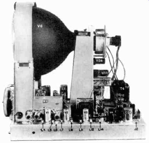
Figure 30. Main chassis of Scott Model 13-A.
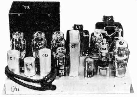
Figure 31. Power supply chassis.
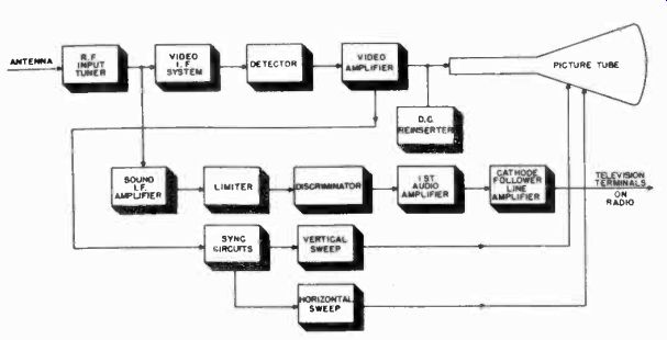
Figure 32. Block diagram of main chassis.
The main chassis contains the RF input circuit, the video IF amplifier, video detector and amplifier, the FM sound IF amplifiers and detector, the vertical sweep circuits, horizontal sweep circuits and audio amplifiers.
A single multiconductor cable which is permanently attached to the power supply and plugs into the male connector on the main chassis connects the two chassis. The only other external connections outside the chassis are the high voltage cable from the power supply to the high voltage connector on the picture tube, and the a-c power cord to the power supply. Figures 30 and 31 show the arrangement of components on the two chassis.
A block diagram of the min chassis is shown in Figure 32.
The component circuits on the main chassis are:
1. R-F tuner.
2. Video IF amplifier and detector.
3. Video amplifier and d-c restorer.
4. Sound FM IF amplifier, limiter, and discriminator.
5. Audio amplifier and cathode follower.
6. Vertical sweep circuits.
7. Horizontal sweep circuits.
7-28 Video Circuits.
The video IF amplifier consists of three over-coupled, wideband circuits employing three 6AU6 high gain pentodes shown in Figure 33. The gain of this system is varied by means of the contrast control R6 which changes the negative bias voltage on the first two video IF amplifier signal grids (V1 and V2). The band of frequencies applied to the video channel is determined by the mixer plate transformer which consists of L1, L2, and L4. Inductance tuning of L1 and L4 is accomplished by means of a movable core which is adjustable from the top of the chassis. The bandwidth of the stage is determined by L2 while the resonant frequencies which are the limits of the band are dependent on L1 and L4. Plate voltage is isolated from the first video IF signal grid by C4. The broad band characteristic of the amplifier stage is enhanced by damping resistors R1 and R4. R2 and C1 are mixer plate supply decoupling components.
The combination C2-L3 is series resonant to the sound IF frequency of 21.9 Mhz, thus permitting the sound IF to be tapped off across L3 and applied to the first sound IF amplifier. This series resonant circuit also prevents sound signals from entering the video channel.
The first video IF tube V1 has both screen and plate voltage removed by the selector switch S 1 when the switch is in the FM position.
The second video IF stage V2 has the same characteristics as the first, except that the associated channel sound trap consisting of C11, C10, and L8 is located in the grid circuit of this stage. This trap operates in the same manner and at the same frequency as the first IF sound trap, C2-L3.
The third video IF stage V3 has no traps and operates exactly as the first and second stages. Variable control grid bias which is applied to the first and second video IF stages is not applied to the third video IF stage. A 1N34 crystal rectifier CR1 is used to detect the video IF carrier and its associated sidebands. R23 is the video detector load resistor. Capacitors C21 and C22 are video bypass capacitors which shunt to ground all frequencies from 30 cps to 4 Mhz.
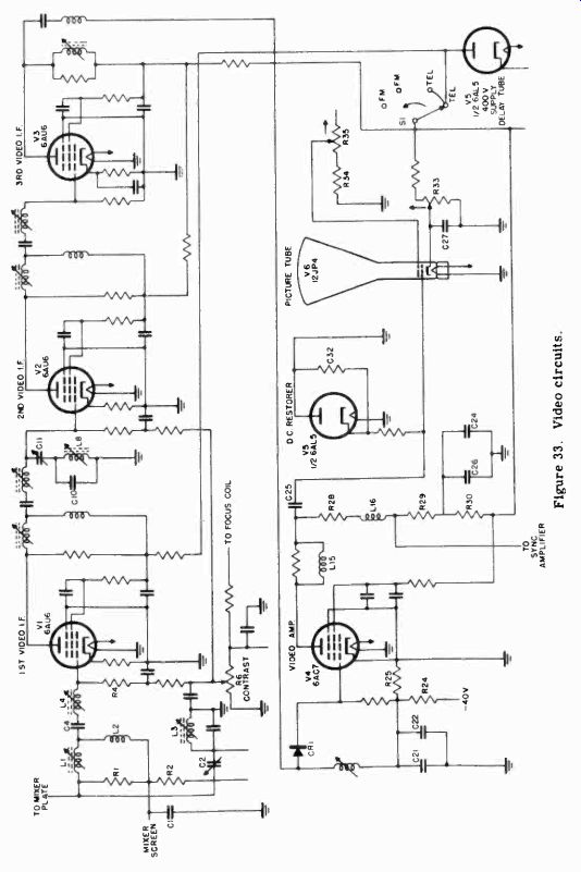
Fig. 33.
The video amplifier uses a high gain pentode V4, compensated to pass a band of frequencies from 30 hz through 4 Mhz. Control grid bias is secured from a voltage divider which is connected across a negative 40 volt supply. This negative voltage is developed across the positioning controls and focus coil which are in series with the ground return of the low voltage transformer. The divider consists of R24 and R25 and provides the proper bias for the video amplifier.
Inductors L15 and L16 are shunt and series components for high frequency compensation. R28 is the load resistor for the tube. Part of the output of the amplifier appears across R29, a portion of the total load resistor. The sync circuits are fed from this point. Plate decoupling and low frequency compensation are provided by R30 and C26 in parallel with C24.
One half of dual diode V5 is used to reinsert the average dc level of the picture which is lost in the capacity coupled video amplifier stage. On negative peaks of the sync signal, capacitor C25 charges to a dc voltage determined by the average brightness of the picture. Resistor R32 is chosen so that the d-c voltage does not change before the next sync pulse occurs.
This dc voltage is applied to the picture tube grid. The 10kv for the second anode of the picture tube is supplied from the power supply chassis. A voltage divider composed of R34 and R35 permits variation of this voltage. R35 is called the drive control and is adjusted so that the control grid cuts off the beam when the minus 50 volts is present on the control grid. This insures that the signal from the video stages will be able to drive the picture to full blackness. The brightness control R33 varies the cathode potential and thus the tube illumination. Capacitor C27 shunts the cathode to ground for all signal voltages.
7-29 Vertical Synchronizing and Sweep Circuits. The video signal and the horizontal and vertical sync pulses are taken from a portion of the video amplifier load R29 and fed through capacitor C62 to the signal grid of the sync amplifier V15, shown in Figure 34. The composite signal is amplified across load resistor R80 and coupled through C63 to the second half of V15 which acts as a sync separator.
Bias voltage for the sync amplifier is secured from a voltage divider consisting of R79 and R78 in series. The sync separator is self biased. Across its load resistor R83 there appear only the vertical and horizontal sync signals, because resistors R81 and R84 reduce the plate voltage of the sync separator so that the tube cuts off the video signals which appear below the sync level. The sync signals appearing at the plate of V15 are applied to the grid of V16 through C64. In the plate circuit across the primary of T2, only the differential of the vertical sync signals appear. The integrating effect of R87, C66, R88, C67, and R89 eliminates the horizontal sync signals.
The vertical sync pulses, applied to the vertical blocking oscillator transformer primary T2, tend to sync the natural frequency of this oscillator to the sync pulses. The operating frequency of the vertical oscillator V16 is determined by R90, R91, C68, and by the vertical sync pulses applied to its control grid.
The vertical hold control, R91, varies the natural oscillator frequency until it locks into the sync pulses.
V16, in addition to acting as a blocking oscillator, also serves as a sawtooth generator. The charging resistors R92, R93 and capacitor C69 determine the size and shape of the sawtooth waveform at the signal grids of V17. Peaking resistor R94 adds a negative peaking pulse to the sawtooth wave at the grid of V17.
The size control R93 varies the amplitude of the waveform on the grid of V17 and thus the vertical height of the picture. Coupling to the grid of V17 is through C70 and R95. Resistors R96 and R97, bypassed by C71A, determine the operating point of V17 and thus affect the linearity. This linearity is changed by R97.
The vertical deflection transformer T3 couples the vertical scanning coil to the dual 6SN7 output amplifier, V17. Positioning of the picture vertically is obtained through the use of control R98 which varies the dc potential across the deflection coil.
7-30 Horizontal Sweep Circuits. The horizontal and vertical sync pulses from the plate of V15, the sync separator tube, are applied to sync clipper tube V18 through capacitor C80 and resistor R140, as shown in Figure 35. The sync clipper tube is self-biased and operates at low plate voltage to provide further clipping of the sync signal and to eliminate video signals which pass through the sync separator. Resistor R141 acts as the plate load resistor, while R102 drops the plate voltage to a low level to provide the proper grid bias for clipping. Capacitor C72 isolates the plate load from R102. The inverted, amplified, and clipped sync pulses are then coupled to a flywheel synchronization circuit. The sync pulses are fed to the center tap of the secondary of phase discriminator transformer Z6 through capacitor C82. An electron coupled oscillator tube, V23, operating at the horizontal frequency (15,750 cps), also is coupled inductively to the secondary of this discriminator transformer.
The primary of this transformer is tuned by a movable core, and the oscillator frequency is varied in this manner. Grid bias for the oscillator is provided by capacitor C86 and resistor R130. R133 is the plate load resistor.
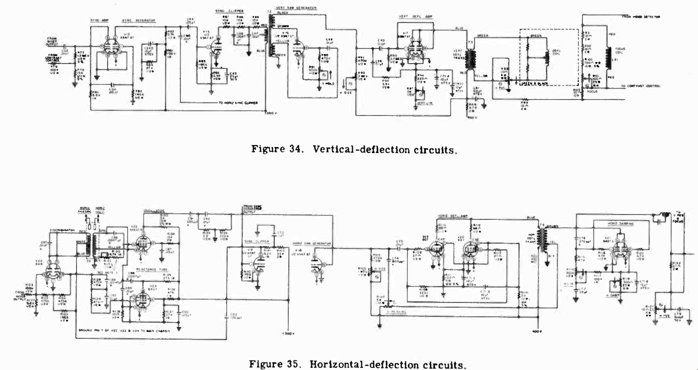
Fig. 34/35
The d-c output voltage developed by the phase discriminator tube V22 is dependent upon the phase difference between the incoming sync pulses and the oscillator signal. This differential d-c voltage is developed across load resistors R126 and R124.
If the oscillator and external sync signals are on frequency and in phase, the net voltage across R126 and R124 is zero. If the oscillator should tend to change frequency or phase with respect to the incoming sync pulses, the differential voltage across R126 and R124 becomes negative or positive depending on the phase shift direction of the oscillator signal. This varying d-c signal is applied to the grid of reactance tube V24, which is in parallel with the primary of the discriminator. The changing reactance of this tube affects the oscillator frequency in such a manner as to bring the frequency or phase of the oscillator back in synchronism with the incoming sync signals. The capacitor C89 tunes the primary of Z6 while C88 couples the reactance tube across the primary.
In order to prevent the oscillator frequency from being disturbed by random noises which come in with the sync signals, a filter is placed across the output load of the discriminator to eliminate these noise signals. This filter consists of R128 and C85, whose time constant is fairly long, so that rapid random noise pulses do not pass through to the reactance tube.
The oscillator plate voltage is differentiated by resistor R138 and capacitor C91 to form sharp negative and positive pulses.
The pulses are applied to the grid of the horizontal sawtooth generator V18 through capacitor C92 and resistor R139. The sawtooth voltage at 15,750 cps is generated across capacitor which is charged through resistors R105 and R106 from the 400 volt supply. The horizontal size is varied by control R106.
R107 varies the negative pulse that is fed back from the secondary of scanning transformer T5. This peaking voltage is combined with the sawtooth on the grids of deflection amplifiers V19 and V20 to provide a peaked sawtooth signal which will produce a linear sawtooth current in the deflection coil.
Two type 807 power tubes are operated in parallel as the deflection amplifier, and are coupled to the deflection coil through output transformer T5. Across the secondary of this transformer is connected a horizontal damping tube, V21, which has two triodes operated in parallel. This tube damps out the natural periodic oscillations of the transformer secondary at the beginning of the trace period. The voltage on the plate of V21 is a negative pulse. This pulse is differentiated by C76, R115 and R116, and applied through R118 and R120 to the grids of V21.
The shape of this grid voltage is determined by the position of the horizontal linearity control R116. This control affects the amount of current drawn by V21 and, therefore, the degree of damping. The net effect is to control the linearity of the saw tooth current in the deflection coil. The horizontal damping control R119 connects both cathodes of V21 to ground. The adjustment of this control affects both linearity and horizontal size by varying the static bias on the cathode of V21. This bias determines the fraction of each cycle during which the damping triode draws current.
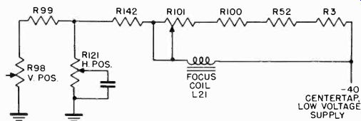
Figure 36. Focus coil circuit.
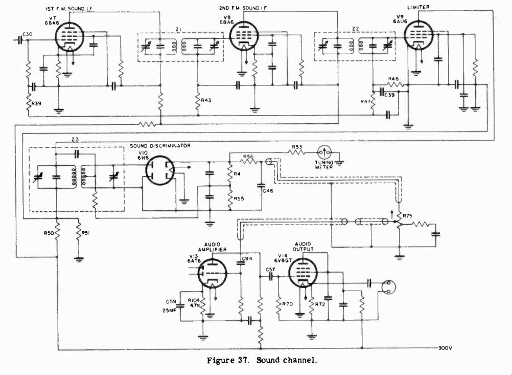
Figure 37
In series with the horizontal deflection coil is resistor R122.
A sawtooth voltage is developed across this resistor by the sawtooth current of the horizontal deflection coil. This saw-tooth voltage is used to trigger the oscillator in the high voltage supply which is described later.
The direct current flowing through the horizontal scanning coil affects the positioning of the electron beam in the horizontal direction. The direct current can be varied by the setting of the horizontal positioning control R121.
7-31 Focus Coil. The focusing coil L21 is in series with the low voltage supply, as shown in Figure 36. The path of the returning current to the power transformer center tap to ground is through the vertical and horizontal positioning controls in parallel, separated by isolating resistor R99; then to a negative voltage takeoff resistor, R142, where the negative voltage bias for the contrast control and sync circuits is obtained; then to the parallel combination of R101 (the focus control) in series with R100. By changing the resistance of the focus control R101, it is possible to vary the current through the focus coil Which is in parallel with it.
7-32 Sound Channel. The sound IF amplifiers utilize two 6BA6 remote cutoff pentodes, as shown in Figure 37. The sound signal at 21.9 Mhz, after being separated from the composite video and audio IF frequencies, is applied through coupling capacitor C30 to the grid of V7. The sound IF transformers are double tuned with variable shunt capacitors. A.V.C. voltage secured from the grid of the limiter stage is applied to both IF stages through isolating resistors R39 and R43.
A 6AU6 pentode tube is used as both a grid and plate limiter, causing limiting on both the positive and negative peaks of the signal voltage. The grid bias and the plate and screen voltages on this tube result in a very short operating curve. The combination of R48 and C39 provides negative grid bias dependent on incoming signal level. Their values are chosen to provide fast limiting on noise impulses. The 300 volt supply voltage is reduced by a voltage divider composed of R50 and R51, to provide a low plate and screen voltage for the limiting tube.
A 6H6 diode tube V10 is used as a conventional balanced discriminator. Both the primary and secondary of Z3 are tuned 20 21.9 Mhz, and are capacitively and inductively coupled to one another. The audio output voltage is dependent upon the frequency deviation from the center frequency of 21.9 Mhz. A tuning meter is connected to one cathode of the discriminator and indicates the d-c voltage appearing across the discriminator load resistors. This d-c voltage is indicative of proper or improper tuning of the signal. As the receiver tunes across the sound carrier, the meter deviates plus and minus from zero reading. When the receiver is properly tuned, the d-c voltage across the discriminator is zero, and the meter shows no plus or minus deviation. The discriminator transformer is linear to plus and minus 75 khz from 21.9 Mhz, and is usable to 100 khz on either side of zero center. Resistor R53 limits the current through the tuning meter, while R54 and R55 are discriminator load resistors.
A de-emphasis network, consisting of R56 and C46, produces an attenuation of the higher audio frequencies to compensate for pre-emphasis at the transmitter. The audio voltage is then passed to volume control R75, and thence to the first audio amplifier.
The triode section of the 6AT6 voltage amplifier, V13, is used to amplify the audio voltage. The signal is fed to the grid of V13 through C94. Bias for the tube is provided by a 4700-ohm cathode resistor bypassed with a 25 mf capacitor, to prevent low frequency discrimination. Capacitor C57 and resistor R70 couple this amplified audio voltage to the control grid of V14, which is a 6V6 operated as a cathode follower. This tube is connected as a triode with its screen grid attached to its plate to reduce the plate impedance of the tube. Output is taken from across cathode resistor R72. The impedance at the cathode is low enough in value to permit attaching a connecting audio cable to the audio system in the Scott AM radio.
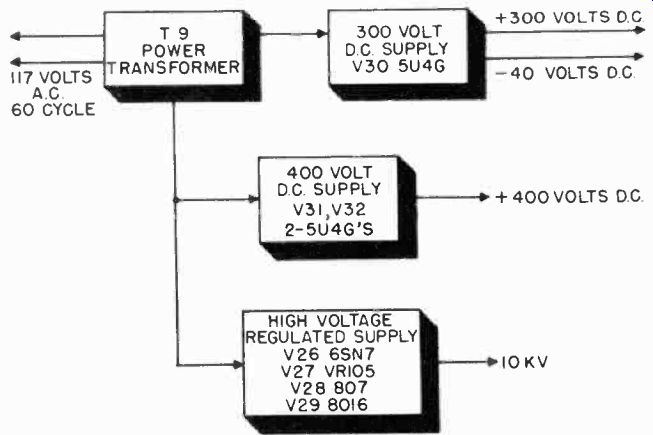
Figure 38. Block diagram of power supply chassis.
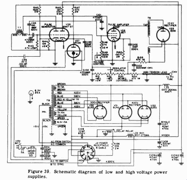
Figure 39
7-33 The Power Supply Chassis. A block diagram of the circuits located on the power supply chassis is shown in Figure 38, while the complete schematic circuit is shown in Figure 39.
The power supply consists of three sections, a 300-volt d-c supply, a 400-volt d-c supply, and a 10 kv high voltage d-c supply. The 400-volt supply is used for the sweep amplifiers and for the high voltage supply circuits. The 10 kv is used as the accelerating potential on the second anode of the picture tube.
The 300-volt supply serves the remainder of the receiver.
The power supply is so designed that if the 300-volt supply should fail, the 400-volt supply immediately becomes inoperative. The 10 kv supply is also shut off in as much as it receives its power from the 400-volt supply. This receiver is equipped with a unique high voltage supply cutoff circuit, consisting of delay diode V5, located on the main chassis, relay K1 (Figure 40) on the power supply chassis, and the service selector switch on the main chassis. This circuit serves three main functions.
It turns off the 10 kv source of high voltage for the picture tube, shuts off the sweep circuits, and disconnects the first video IF amplifier voltages when the selector switch is in the FM position.
When the service selector switch is in the video position, a 300-volt d-c voltage is applied to the diode delay tube V5. The diode therefore draws current, energizing the 400-volt delay relay K1, and applying 400 volts d.c. to the high voltage and sweep circuits. If the service selector switch is in the FM position, the diode is not supplied with 300 volts and consequently the 400-volt delay relay is not energized. This leaves the high voltage and sweep circuits without voltage and permits listening to FM without the scanning raster appearing on the picture tube.
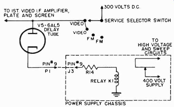
Figure 40. Automatic, high-voltage cutoff circuit.
The second-purpose of the delay tube is to protect the fluorescent screen of the picture tube. In the above discussion, it was noted that relay K1 must be energized in order for the sweep circuits and the high voltage circuits to operate. When the set is turned on, there is a period before the delay tube warms up.
Therefore, no high voltage will be generated until the end of this warm up period. This delay gives the sweep circuit tubes a chance to warm up before the high voltage is applied to the picture tube. Scanning current therefore flows through the deflection yoke before the high voltage comes on. If this were not the case, the high voltage applied to the picture tube without deflection currents in the yoke would cause a bright spot on the screen. if a spot occurred for any length of time, it would damage the screen material.
A third function of the delay tube is to allow the tubes to warm up properly before voltage is applied to the filter capacitors.
This protects the capacitors against excessive voltage, which would exist during the warm up period when the tubes are not drawing B+ current from the supply.
7-34 300-Volt Supply. The 115-volt, 60-cycle, a-c current passes through a 5 amp fuse, F1, 4 and 2 pins of plug J2, an interlock switch, S3, then through the connecting cable between chassis, to the on-off switch on the main receiver chassis, back to the power supply chassis, through the primary of the power transformer, and back to the a-c line. The interlock switch is so located on the power supply chassis that when the back panel of the receiver is removed, the switch is opened and the set automatically shut off. Thus no harm can come to an inexperienced person who opens the receiver and attempts to tamper with the circuits. When servicing a receiver with an interlock switch, the technician must temporarily short the switch terminals.
The single 5U4G rectifier tube, V30, has a separate filament winding, while its plates are connected to the 380-volt taps of the transformer secondary, as shown in Figure 39. A single section pi filter is utilized with capacitor C107 acting as the input filter. This capacitor is not grounded at the negative terminal, but connects to the negative electrode of capacitor C108 which shunts all a-c signals and sweep voltages across the negative bias supply to ground. Filter inductor L23 and capacitor C109B provide additional filtering. The 300-volt d-c voltage is then fed to pin 1 of J2 on the power supply chassis.
7-35 400-Volt Supply. A second filament winding supplies two 5U4G rectifier tubes with filament power while their plates are connected to the 425-volt taps on the power transformer secondary. The first filter capacitor, C106, is isolated from the rectifier tubes by delay relay Ki, which allows the sweep and high voltage tube filaments time to warm before voltage is applied to capacitor C106. This capacitor is returned directly to the negative side of the supply. Filter inductor L22 terminates in filter capacitor C109A,'the negative side of which is grounded.
The 400-volt d-c voltage is then connected to pin 5 of J2 on the power supply chassis.
7-96 High Voltage Supply. A block diagram of the high voltage supply is shown in Figure 41. The high voltage supply is of the high frequency pulse type. One half of V26, a 6SN7 tube, is used as a pulse generator to create the sharp high voltage pulses which are applied to the grid of V28, on 807 pulse amplifier tube. The blocking oscillator, V26, is normally biased to cutoff so that no current flows and no pulses are generated.
The tube is triggered into operation by a sawtooth voltage which is applied to its cathode through R145 (Figure 39). This saw tooth voltage, which occurs at 15,750 cps, is developed across resistor R122 (Figure 35) in series with the horizontal deflection coil.
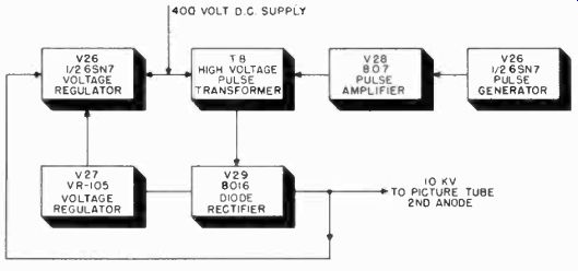
Figure 41. Block diagram of 10KV high voltage supply.
When this sawtooth voltage is fed to the cathode of V26, the blocking oscillator conducts and produces pulses of short duration. These pulses appear on the grid of V28. Resistor R150 and capacitor C102 provide bias for this pulse amplifier tube.
The plate of V28 is coupled to an autotransformer T8 with a high voltage step-up winding. The pulses are increased to approximately 10 Kv by this autotransformer. The high voltage pulses occur at 15,750 cps and are rectified by V29, an 8016 diode. Filament power for V29 is obtained from the high voltage autotransformer by coupling a few turns to its primary. The high voltage is filtered by a two section filter. R155 and C103 comprise the first section, while R154 and the capacity of the high voltage coaxial cable, which carries the high voltage to the picture tube, act as the second filter section.
To minimize the effects of line voltage variations on the output of the high voltage supply, a regulator circuit, consisting of V27 and one half of V26, is used. A portion of the high voltage is tapped across the high voltage bleeder, consisting of R153 in series with R152 and R151. This voltage is fed to the grid of a regulator tube, the second half of V26. The amount of current which this tube draws determines the screen voltage of the pulse amplifier V28, and hence affects the amplitude of the high voltage pulses. A VR-105 tube, V27, is used in the cathode of the regulator tube to hold this voltage constant. All current variations through the tube are then due only to the grid voltage variations.
The regulator circuit operates in the following manner to maintain constant high voltage d.c. Assuming that the high voltage output decreases (caused by an increase in line voltage), the portion fed back to the grid of the regulator tube, V26, also decreases, thereby decreasing the current through R146 and the voltage drop across R146. The screen voltage of the pulse amplifier tube immediately increases and the high voltage output increases to maintain the original operating voltage.
Another feature of this high voltage circuit is the automatic cutting off of the high voltage if the horizontal sweep should fail.
If no horizontal sweep voltage is generated, no sawtooth voltage is fed to the cathode of the first half of V26. The pulse generator is then biased to cutoff and no pulses or high voltage are produced.
7-37 DuMont Model RA-101. The Du Mont Model RA-101 is an example of a complete console receiver containing facilities for television, FM and AM reception, and an automatic record changer. The Model RA-101 circuits appear in both the Du Mont 15-inch tube models and the 20-inch tube models.
This receiver consists of several chassis and sub-assemblies, as follows.
1. The RF/ IF chassis, containing both sound and video IF circuits, video amplifier, and RF tuning system.
2. The sweep chassis, containing sweep circuits, a power supply for low voltage, and the high-voltage supply for the picture tube. A sync stabilizer sub-chassis, containing an automatic frequency control circuit for the horizontal sync system.
3. The AM tuner chassis, containing the tuning unit for AM reception.
4. The audio amplifier chassis, containing the audio amplifier and its own power supply. All sound facilities of the receiver use this amplifier.
5. The tuning meter assembly, containing the tuning meter for the television and FM sound plus the cable connecting it to the RF/ IF chassis.
6. The tone selector assembly, consisting essentially of a push-button switch and the tone control components.
7. Picture tube assembly, consisting of the cathode-ray tube, focusing coil, and deflection yoke.
8. The service selector switch assembly, consisting of a push-button switch system, which selects either one of the facilities.
9. The record changer.
A block diagram off the receiver showing the relationship of the various circuits is given in Figure 42.
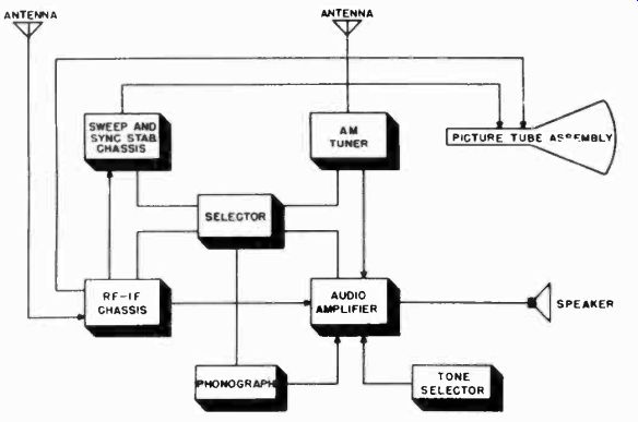
Figure 42. Block diagram of DuMont Model RA-101
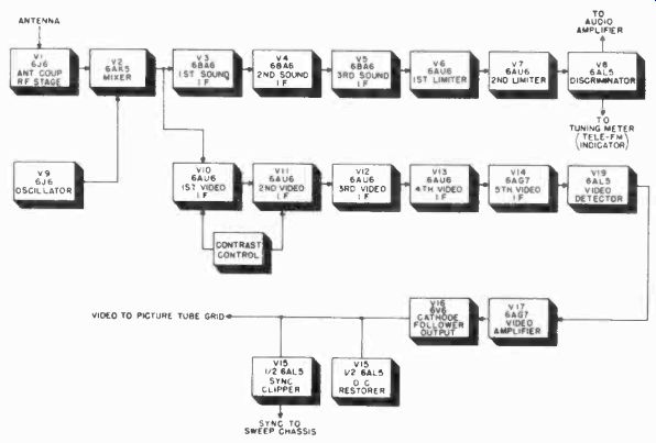
Figure 43. Block diagram of RF, IF chassis.
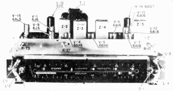
Figure 44. R-F, I-F chassis showing slide-rule dial. (courtesy DuMont)
7-38 RF/IF Chassis. A block diagram of the circuits located on the RF/ IF chassis is shown in Figure 43. This receiver employs the Du Mont Inputuner described at the beginning of this section. This tuner is the same one which is used in the Scott receiver previously described. There is one difference between the two. The tuner dial in the Scott receiver is manually rotated, whereas a motor drive is provided on the Model RA-101. A slide rule dial (Figure 44) is used on this model rather than rotating discs employed on the Scott receiver.
The pointer travels from the low frequency (channel 1), lower right hand side of the dial, to the lower left hand side. When it reaches the left side of the dial it makes a U turn and continues traveling from left to right along the upper scale of the dial till it reaches channel 13. A slipping clutch is built into the motor drive so that when the pointer reaches the end of its travel at either the low frequency or high frequency ends, it cannot be damaged.
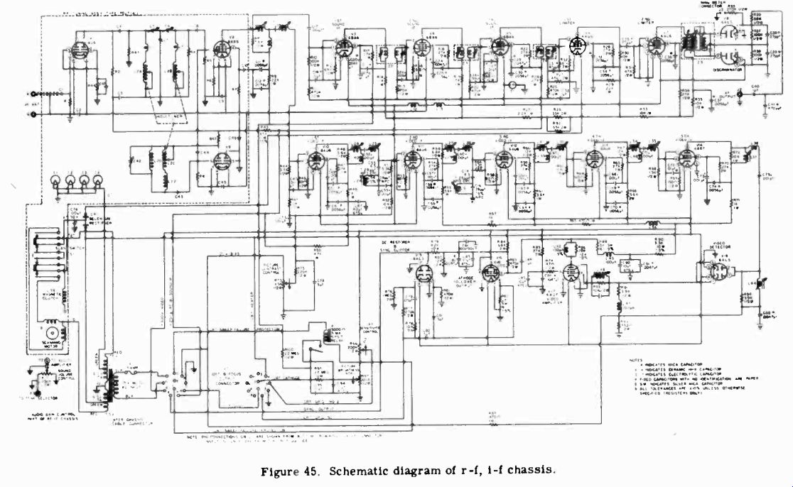
Figure 45
Tuning is accomplished by closing a switch on the motor. The operator holds the switch closed until the pointer travels to the desired station. A vernier tuning knob is geared to the motor drive for precise manual adjustment to the station frequency after the motor has moved the pointer to the station.
The tuned circuit in the plate of the mixer tube (Figure 45) is tuned to have a band pass of 21.5 to 26.4 Mhz. The sound IF frequency is picked off prior to the tuned circuit and the video IF frequency passes through to the grid of V10, the first video IF amplifier. Five broad-band coupled video IF amplifier stages are provided. These five stages consist of V10, V11, V12, V13, and V14. All stages employ 6AU6s, except V14 which uses a 6AG7. The over-coupled transformers between stages are each tuned to provide a band pass of 4 Mhz. Two sound traps are employed, one in the grid of the second video IF stage V11, and one in the grid of the third stage V12. These sound traps prevent the sound IF signals from passing through the video IF amplifier.
The output of the fifth video IF stage, V14, feeds V19, the video detector. V19 is a dual diode connected as a push-pull detector. The detected output is applied to the grid of the first video amplifier, V17, a 6AG7. V17 in turn feeds V16, a 6V6, connected as a cathode follower output stage. The output of V16 is coupled directly to the grid of the picture tube. One section of V15, a dual diode 6AL5, is connected across the output of V16, to act as a d-c restoration circuit. The other half of V15 is a diode sync clipper. It too is connected across the output of the cathode follower and is biased so that conduction takes place only when the sync signals occur. The video portion is thus effectively clipped. The sync signal is taken from the plate of the sync clipper, and is fed to the sweep chassis in composite form.
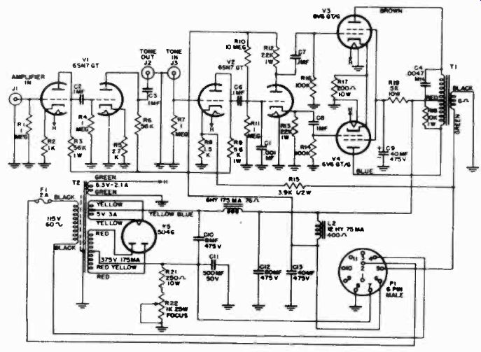
Figure 46. Audio amplifier schematic.
The sound IF amplifier is a three-stage amplifier consisting of V3, V4, and V5, type 6BA6 tubes. The interstage transformers are over-coupled and have uniform response over a 200 khz pass band. After passing through the sound IF amplifiers, the sound signal is fed to two limiter stages, V6 and V7, which are connected in cascade. These tubes remove amplitude modulation from the FM signal. The output of the second limiter is coupled to the discriminator by means of transformer Z5. The discriminator, V8, is a conventional balanced type, and is tuned for zero output voltage at the sound carrier IF frequency of 21.9 Mhz. A tuning meter (similar to the type used with the Scott receiver) is connected to one of the cathodes of the discriminator and registers zero when the FM or television station being received is properly tuned. The output of the discriminator is the audio signal which is fed to the audio amplifier chassis for further amplification.
There are a number of other components located on the RF/ IF chassis. These items are enumerated below.
1. The Contrast Control, R73, varies the video IF amplifier gain by changing the negative bias voltage applied to the grids of the first two video IF amplifiers.
2. The Picture Brightness Control, R97, is located on this chassis. It sets the positive d-c voltage applied to the cathode of the picture tube and so determines the intensity level of the picture.
3. The Sound Volume Control, R17, is also located on this chassis to consolidate all controls on a single chassis. R17, which is a gain control in one of the audio circuits located on the audio chassis, is connected by shielded cable from the RF/ IF chassis to the audio stage.
4. The motor drive switch and the hand vernier tuning mechanism are also included on this chassis for further consolidation of controls on the front panel of the receiver.
7-39 The A-M Tuner Chassis. The AM tuner chassis, which is employed in the Model RA-101, consists of a conventional AM receiver except for the audio output stage. A single RF stage, a converter, IF amplifier, and detector are provided. A 6SA7 serves the function of both oscillator and mixer to convert the RF signal to an intermediate frequency of 456 khz. Another 6SK7 serves as the IF amplifier, which feeds a dual triode 6SN7. The first section of the 6SN7 is connected as a diode and acts as a detector. The other half is operated as a triode cathode follower which couples the audio signal to the audio amplifier chassis.
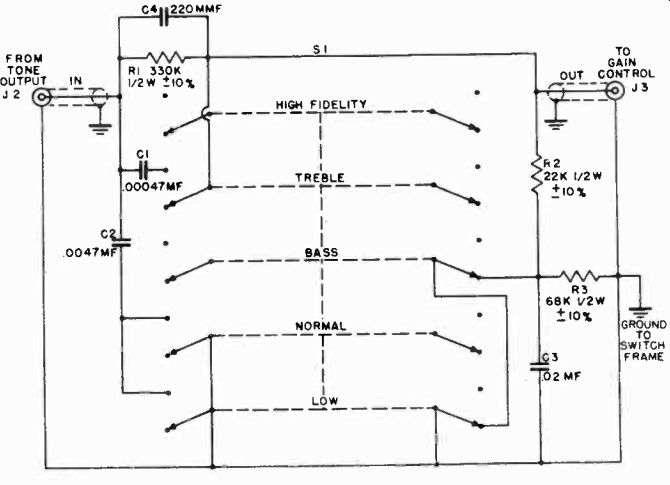
Figure 47. Tone selector schematic.
7-40 The Audio Amplifier Chassis. The audio amplifier (Figure 46) consists of four tubes, two type 6SN7s, and two type 6V6s. All stages in the amplifier are resistance coupled. V1 is a dual triode, both sections of which are connected as voltage amplifiers in cascade. The volume control is connected in the input circuit of the first stage and is located on the RF/ IF chassis. The tone control is connected in the plate circuit of the second half of V1. Any one of five tones may be selected by means of a tone selector switch (Figure 47), connected across J2 and J3 in the plate circuit. The tone selector is a separate assembly with five different RC circuits which vary the response of the amplifier. This separate assembly is located on the front panel of the receiver with the rest of the operating controls.
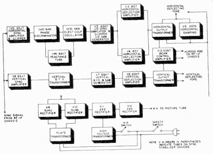
Figure 48. Block diagram of sweep chassis.
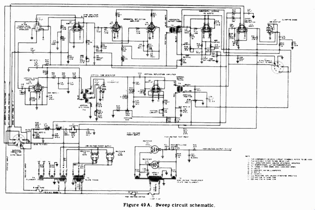
Figure 49.
The output of the tone circuit is fed to the first half of V2, another voltage amplifier. This stage in turn feeds the second half of V2, which is a phase inverter. Since the voltages on the cathode and plate of an amplifier are 180° out of phase, signals may be taken from these points to drive a push-pull circuit.
The plate resistor, R12, and the cathode resistor, R13, are so chosen that the voltage output from the cathode and plate are of the same amplitude. These voltages, which are 180° out of phase, are applied to push-pull 6V6s, V3 and V4. The push-pull output stage is coupled to the speaker through transformer Ti.
7-41 The Sweep Chassis. The sweep chassis contains the power supply which furnishes B+ and bias voltages to the sweep circuits and to the circuits on the RF/ IF chassis. A block diagram of the circuits located on the sweep chassis is shown in Figure 48. The low voltage power supply contains two 5U4G rectifiers, V9 and V10 as shown in Figure 49A. A time delay relay, K1, in this supply prevents B+ from being available for about 30 seconds after the set is turned on. This time delay permits the filament to warm up so that the tubes immediately conduct when the B+ is applied. Otherwise, the load on the power supply would be low when the set is first turned on and the B+ voltage would rise above the safe operating voltage of the filter condensers. The filter section consists of L1, L2, C19, and C33. The voltage between L1 and L2 is higher than the output of the filter. This higher voltage is used for vertical and horizontal sweep amplifier stages while the lower voltage of 300 volts is used for the rest of the receiver.
The sweep chassis also contains the high voltage power supply.
This power supply is of the 60-cycle type and uses two type 2X2 rectifiers, V11 and V12. The rectifier tubes are connected in a voltage doubler circuit to provide 12 kv d-c output. On the negative half of the a-c cycle, V11 conducts and condenser C34 charges to 6 kv. This charge is applied to the plate of V12. On the positive cycle, V12 conducts and charges C35. The voltage on C34 is added to the charge on C35, producing 12 kv across this condenser.
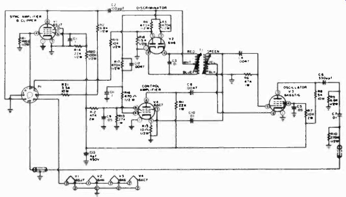
Figure 49B. Sync stabilizer schematic.
The clipped sync signal from the RF/ IF chassis is fed to V6, a 6SJ7. This tube amplifies the vertical sync signal. An integrating circuit (R25, R26, R24, C16, and C17) in the plate circuit of V6 separates the vertical sync pulses from the horizontal sync pulses. The vertical sync signal is applied to the blocking oscillator, one half of V7, through a sync winding on the oscillator transformer. The sync pulse is coupled by the transformer to the grid of V7 and locks the oscillator into synchronism. The oscillator and sawtooth generator functions are combined in this stage.. The charging circuit is located in the plate circuit. C20 is the charging condenser, which is charged through R33 and R30. The vertical sawtooth voltage developed across C20 is fed to deflection amplifier, V8, a dual triode with both halves operating in parallel. The vertical deflection amplifier drives the primary of T4, the vertical output transformer.
The secondary of T4 is coupled to the vertical deflection coil.
Vertical positioning is obtained by means of a potentiometer, R36, which injects a negative d-c voltage into the deflection coil.
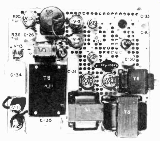
Figure 50. Sweep chassis. (courtesy DuMont)
The horizontal sweep circuit is very similar to the type in the Scott Model 13-A, already described. Flywheel synchronization is employed to stabilize the sync system. The clipped sync signals coming from the RF/ IF chassis are first amplified by V1, a 6SJ7 sync amplifier (Figure 49B). These signals are then fed to the sync discriminator transformer. The flywheel sync circuit is identical in design to that found in the Scott receiver. V3 is the Hartley oscillator, V2 the discriminator, and V4 the reactance tube. A stabilized triggering pulse is obtained from the circuit in the plate of V3. This triggering pulse is applied to the second half of V2, the horizontal sawtooth generator. The remainder of this circuit is again similar to the Scott horizontal sweep circuit. The sawtooth voltage is developed across C5 and applied to two 807 deflection amplifier tubes, operated in parallel. The output of the 807s is coupled to the deflection coil through T2. V5 is a 6AS7G, operated as a triode damper.
The layout of the sweep chassis is shown in Figure 50. Note the holes punched in this chassis to help dissipate the heat generated in the power supply and sweep components.
7-42 The Picture Tube Assembly. The picture tube for the 20-inch versions of the model RA-101 is the type 20BP4. Since the 20-inch tube is about 29 inches long, it is mounted vertically in a cradle. The picture tube, its focusing coil, and its deflection yoke are all mounted in the cradle. This cradle is raised into a horizontal position for viewing by a mechanical driving mechanism. To bring the tube into the horizontal position, the lid on the cabinet is raised. This automatically throws a switch which starts the lift mechanism.
The picture tube used in the 15-inch versions of the model RA-101 is the type 15AP4. It is mounted in a fixed horizontal position in the cabinet and is not provided with a tilt mechanism.
7-43 RCA Victor Model 648 PTK. The RCA model 648PTK is a forty-eight tube projection television, AM/ FM radio, console receiver. The television receiver employs four chassis with a total of thirty-five tubes, plus a five-inch projection tube.
These chassis are:
1. An RF/ IF chassis which includes the RF tuner, the video and sound sections, and the vertical sweep circuits.
2. A chassis on which is mounted the horizontal sweep system and the 27 kv high voltage supply, which is a part of the horizontal sweep circuit.
3. A low voltage power supply chassis which furnishes power to the entire receiver.
4. An audio amplifier which is switched into the sound circuits of either the television, FM or AM sections of the receiver.
The four chassis are located in a large console as shown in Figure 51. The heavy black lines indicate the interconnecting cables. In the lower right hand corner is the optical barrel which houses the projection tube and optical components of the Schmidt reflective system, which is employed in this receiver.
A 15-inch by 20-inch picture is obtained on the screen.
The reader will note in the following description of the 648PTK that the RF and video circuits are similar to those found in direct view receivers which produce smaller pictures. Only in the horizontal deflection circuits and the high voltage power supply are there radical departures from direct view receiver designs. The latter circuits differ only because the projection tube must operate at higher voltages and therefore requires greater deflection power.
A block diagram of the Model 648PTK is shown in Figure 52.
This receiver employs the RCA 13-channel switch type tuner described earlier in this section.
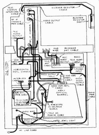
Figure 51. Arrangement of chassis in RCA console Model PTK. (courtesy RCA)
7-44 Video Channel. The picture IF amplifier is of the stagger tuned type. To obtain the necessary wide band characteristic with adequate gain, four stages of IF amplification are employed, as shown in Figure 53. The converter plate and each successive IF transformer utilize one tuned circuit each, and each is tuned to a different frequency. The effective Q of each coil is fixed by the shunt plate load or grid resistor so that the total response of all the stages produces the desired overall pass band. Figure 54 shows the relative gains and selectivities of each coil and the shape of the curve formed by the combination of stages.
In order to obtain this band pass characteristic, the picture IF transformers are tuned as follows:
Converter transformer 21.8 Mhz (T2 primary)
First picture IF transformer. 25.3 Mhz (T4 primary)
Second picture IF transformer 22.3 Mhz (T105 primary)
Third picture IF coil 25.2 Mhz (L104)
Fourth picture IF coil 23.4 Mhz (L106)
In such a stagger tuned system, variations of individual IF amplifier tube gain do not affect the shape of the overall IF response curve if the Qs and center frequencies of the stages remain unchanged. This means that the IF amplifier tubes are non-critical in replacement because variations in Gm do not affect the response curve.
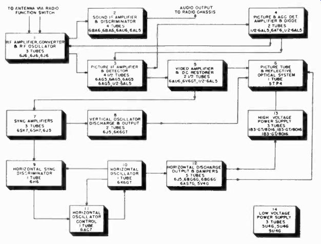
Figure 52. Block diagram of Model 648 PTK.
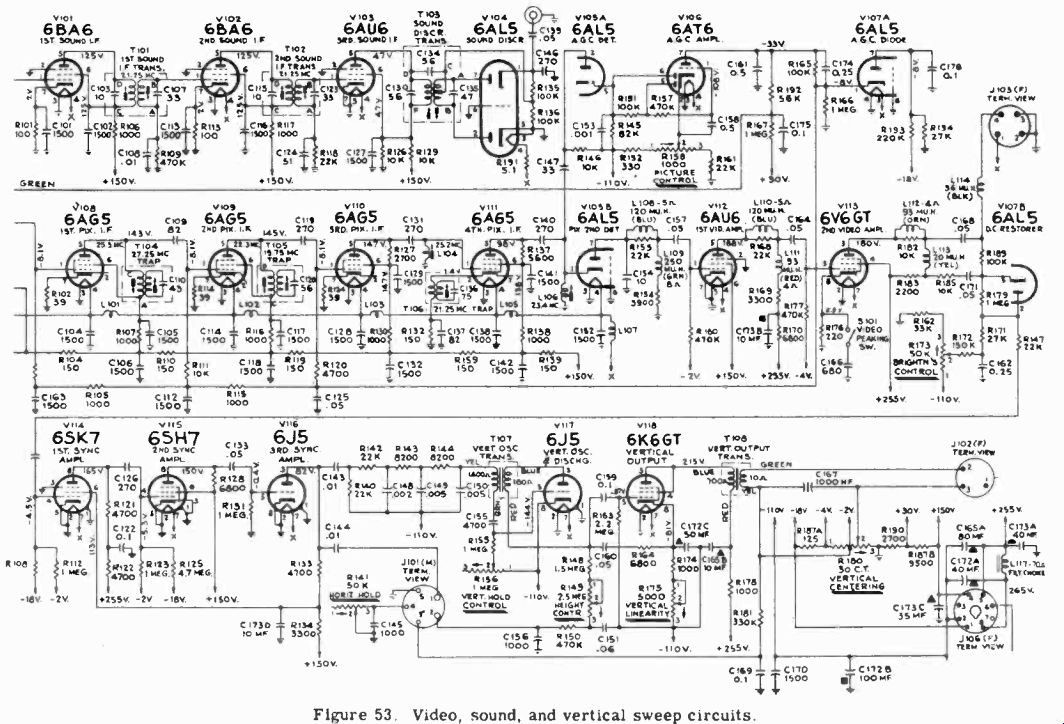
Figure 53.
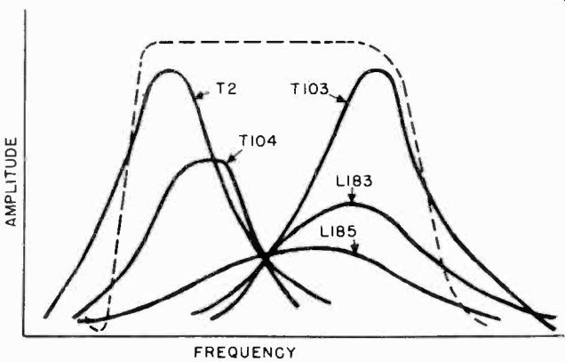
Figure 54. Relative gain and selectivity of each coil in staggered IF amplifier.
Resulting overall response curve is shown dotted in background.
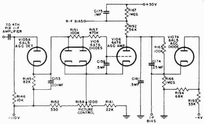
Figure 55. A.G.C. circuit.
Four traps are used to shape the IF response curve and attenuate the sound signals, and the adjacent channel picture carrier. The first trap (T2 secondary) is tuned to the accompanying sound IF frequency. The second trap (T104 secondary) is tuned to the adjacent channel sound frequency. The third trap (T105 secondary) is tuned to the adjacent channel picture carrier frequency. The fourth trap (T106 secondary) is in the cathode circuit of the fourth picture IF amplifier V111, and is tuned to the accompanying sound IF carrier. The primary of T106, in series with C 137, forms a series resonant circuit at the frequency to which L106 is tuned (23.4 Mhz). This provides a low impedance in the cathode circuit at this frequency and the gain of the tube is high. However, at the resonant frequency of the secondary (21.25 Mhz), a high impedance is reflected into the cathode circuit, reducing the gain of the tube. At 21.25 Mhz, therefore, the response curve takes a decided dip.
The 6AL5 detector, V105B, is a conventional half-wave rectifier connected to produce a video signal of negative polarity.
7-45 A.G.C. Circuit. An automatic gain control circuit is employed in connection with the picture IF system to hold the output from the IFs substantially constant over a wide range of signal inputs.
In the a.g.c. system of the picture IF amplifier (shown in Figure 55) a portion of the output from the fourth IF amplifier is fed into V105A, the a.g.c. detector. Since the time constant of the diode load resistor and filter (R145 and C153) is somewhat greater than one horizontal line, the detector is essentially a peak reading voltmeter at sync frequency. The d-c voltage that appears on the cathode of V105A is therefore proportional to the peak strength of the received signal and is substantially independent of the picture content.
Such a system will also tend to read the peak of noise pulses.
To prevent this, R151 and the diodes of V106 are used as a two stage clipper or noise limiting network. For further protection against noise, the d-c output is fed through an integrating network (R157 and C158) which tends to minimize the effect of random noise.
The d-c output from the integrator is less than that required to control the gain, and since it increases in the positive direction with increase in signal strength, it is necessary to amplify and invert it. To accomplish this, the output from the integrator is d-c coupled to the grid of V 106, the a.g.c. amplifier. V106 is operated with approximately minus 110 volts on its cathode, and with its plate at or slightly below ground potential. The voltage available at the plate is suitable for use as a control bias.
With a weak signal input, the bias on V106 (obtained across R152 and 1(158) is sufficient to cause the plate current of V106 to be nearly cut off. The plate of V108 is at approximately ground potential, no bias is applied to the RF and IF grids, and the receiver operates at maximum gain. When a strong signal is applied to the receiver, the d-c output from the a.g.c. detector opposes the fixed bias on V106 and causes more plate current to flow. As a consequence, the plate goes negative with respect to ground and this negative voltage is applied to the RF and IF grids, reducing their gain and maintaining constant output from the IF system.
Since the grid control characteristic of pentode IF amplifiers is different from that of the triode RF amplifier in the tuner, different bias voltages are required and must be taken from different points in the system. The RF bias is taken from the junction of R165 and R166.
In order to obtain the maximum signal-to-noise ratio from the receiver, it is desirable to allow the RF amplifier to run at full gain on any signal which will not cause overloading of the first IF stage. The circuit arrangement of Figure 5.5 including the a.g.c. diode, V107A,permits maximum use of RF gain on weak signals and prevents overloading of the IF amplifier on strong signals. With an input signal of 1000 microvolts (and the picture control set for normal contrast) the plate of V106 is at approximately-2 volts. Since the a.g.c. diode plate is placed at a-2.5 volt tap on the dividers R193 and R194, the diode does not conduct and the-2 volts on the V106 plate is applied to the IF grids. With a signal of 10,000 microvolts, the a.g.c. amplifier plate is at approximately-5 volts. Under this condition, the a.g.c. diode conducts and due to the drop in R165, prevents the IF bias from rising appreciably above-3 volts.
A manual gain control, R158, is also provided since it is necessary to vary the picture contrast because of variations in room lighting, transmitting technique, and to suit personal preference in picture balance. The control varies the IF gain by varying the initial bias on the a.g.c. amplifier, which in turn varies the RF and IF bias.
The detected video signal is fed to two stages (V112 and V113) of video amplification (Figure 53). A noise saturation circuit is incorporated into the video amplifier. The first stage V112 is designed so that with a normal negative signal input level at its grid, the tube will be working over most of its operating range. Any large noise signal above the sync level will drive the grid to cutoff and the noise will be limited. In effect, the signal-to-noise ratio is improved and better synchronization results.
Since the video amplifier is an a-c amplifier, the d-c component of the video signal that represents the average illumination of the original signal will not be passed. The 6AL5 d-c restorer V107B reestablishes the d-c level and provides a bias on the picture tube grid that varies-with the scene.
7-46 Optical System. The picture tube employed in this receiver is a 5TP4, five-inch projection tube, used with a Schmidt reflective system. The tube operates at approximately 27 kv and employs magnetic deflection and electrostatic focusing. The tube and deflection yoke are mounted in an optical barrel.
This barrel also supports a spherical mirror at the bottom, and a corrector lens at the top. The image formed on the picture tube is projected onto a 45° mirror and then onto a translucent screen. The screen is composed of two Lucite sheets, with a partial diffusing layer between them. The back sheet has tiny lenses molded into its rear surface. The front sheet has vertical ribs molded into its outer surface. This combination of lenses and ribs transmits five times more light than a ground glass.
7-47 Sweep Circuits. The signal from the d-c restorer is fed to a sync amplifier, V114 (Figure 53), which is a 6SK7 with a remote cutoff characteristic. The video signal at the grid of V114 is negative, so that any noise signals above sync which remain after the limiting action of the first video grid are further compressed when they drive the grid beyond the cutoff point.
The output of this stage, which is positive in polarity, is fed to the grid of V115, another sync amplifier. The operating voltages applied to the grid and plate of this amplifier are such that the negative portion of the applied signal is cut off. Thus, the video and blanking pulses are removed and only the sync pulses appear at the plate.
The sync pulses are further amplified by V116. Since they are negative in polarity on the grid, they appear positive at the plate. This is the required polarity for triggering the sweep oscillators. The signal at the grid of V116 is sufficient to drive the tube beyond cutoff and the signal is again clipped. This final clipping removes all amplitude variations between sync pulses due to noise, hum, etc.
The vertical sync pulses are separated from the horizontal sync pulses by the integrating network consisting of R142, R143, R144, C148, C149 and C150. A single 6J5 triode, V117, with its associated components, forms a blocking oscillator and discharge circuit. The vertical sync pulse from the integrating network is applied to the grid of V117 and locks the oscillator to the vertical frequency.
On the plate of V117, a sawtooth voltage appears due to the slow charging and rapid discharging of C 160. A sharp negative pulse also occurs during the discharge period because of the peaking resistor R164 in series with C160. C160 charges through R148 and R149. Adjustment of the height control R149 varies the amplitude of the sawtooth voltage on the plate of V117 by controlling the rate at which C160 can charge. The voltage present on the plate of V117 is of the shape required to produce a sawtooth current in the vertical deflection coil. It is now necessary to amplify it in a tube capable of supplying a sufficient amount of power.
A 6K6 is connected as a triode for the output stage, V118. The vertical output transformer T108 matches the resistance of the vertical deflection coils to the plat e impedance of the 6K6. R175 is provided as a vertical sweep linearity control. Since the grid voltage, plate-current curve of V118 is riot a straight line over its entire range, the effect of adjustments of R175 is to produce slight variations in the shape of the sawtooth by shifting the operating point of the tube to different points along the curve. Since the slope of the curve varies at these different points and thus varies the effective gain of the tube, it is apparent that adjustments of linearity affect the picture height, and that such adjustments must be accompanied by readjustments of the height control R149.
The horizontal sweep circuit in the RCA 648PTK is very similar to the flywheel synchronization type described in the Scott Model 13-A receiver. The horizontal sweep circuits are shown in Figure 56. The horizontal oscillator is an extremely stable Hartley oscillator operating at the scanning frequency of 15,750 hz. The primary of T301 (terminals A, B, and C) is the oscillator coil. The coil is closely coupled to the secondary winding (terminals D, E, and F) and thus feeds a sine wave voltage to V301. The sync discriminator V301 is a 6H6 dual diode which produces the d-c output voltage proportional to the phase displacement between the incoming sync pulses and the sine wave horizontal oscillator voltage.
V303 is the reactance tube which controls the oscillator frequency. A change in the d-c output of the sync discriminator produces a change in Gm of V303 which in turn changes the frequency of the oscillator. If the phase of the oscillator shifts with respect to the synchronizing pulse, the corresponding change in output from the sync discriminator causes the oscillator to be brought back into correct phase.
C304 and C306 form a voltage divider to attenuate rapid changes in output from the sync discriminator, such as are produced by the vertical sync pulses or a burst of noise.
The oscillation in V302 takes place between the screen-grid and cathode. Since the peak-to-peak voltage on its grid is as high as 100 volts, overloading takes place and a square wave voltage is produced in the plate circuit. This wave is differentiated by C312 and R314. The pulse so obtained is applied to the grid of the discharge tube V304. The discharge tube is normally cut off during the period that the condenser C318 is charging. Then the pulse from V302 overcomes the cutoff bias and drives the tube into heavy momentary conduction. During this period, C318 charges rapidly. Then, when V304 again becomes non-conducting, the plate voltage rises slowly, and approximately linearly, as C318 charges through R316 and C315.
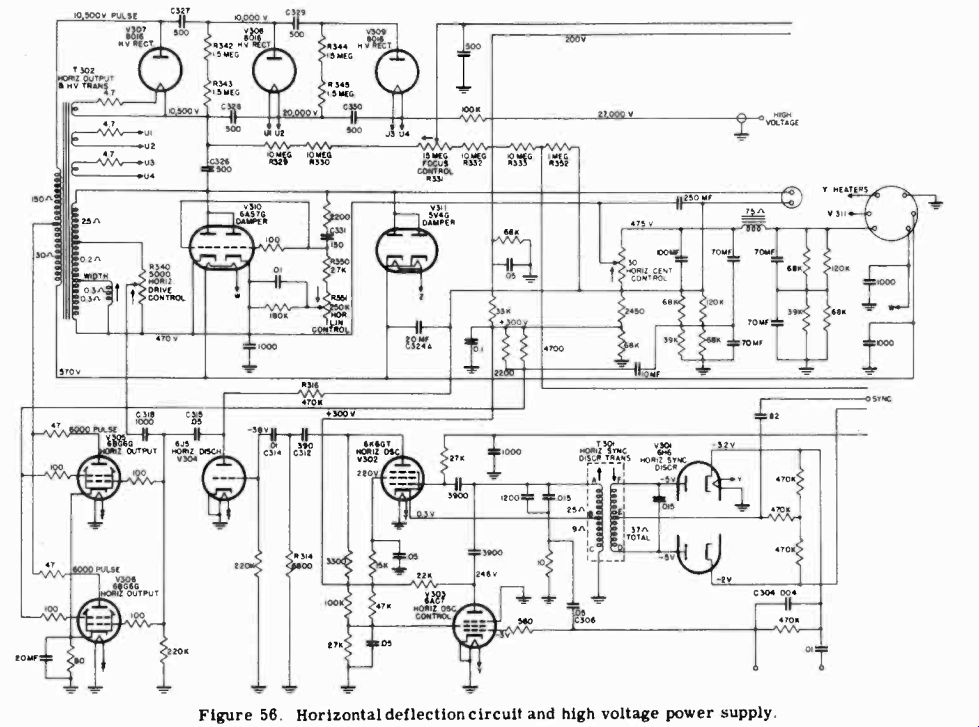
Fig. 56
The output of the discharge circuit is applied to two power amplifier tubes, V305 and V306, connected in parallel. Two such tubes are required to provide sufficient horizontal scanning current in the deflection coil because of the high operating voltage of the 5TP4 projection tube. With 27 kv on the tube, it is more difficult to deflect the electron beam. The horizontal deflection current needed is slightly greater than the capabilities of a single 6BG6 tube. When two horizontal output tubes are employed as in the 648PTK, proper damping cannot be obtained by a single damper tube due to the heavy damping current.
V311, a 5V4G, provides damping action over the entire trace.
V310, a dual triode, is employed to provide the extra damping action during the first portion of the trace when large oscillations occur. When the voltage on the plate of damper tube V310 swings positive during the start of the trace, the differentiating network (C331, R350, and R351) changes this rising voltage to a pulse and feeds it to the grid. This positive pulse lowers the plate resistance of the triodes and permits heavy damping current to flow. Then, due to the short time constant of the grid network, the positive pulse decays and the bias due to the grid rectification of the pulses cuts the triode damper off, leaving the 5V4G to provide the damping for the remainder of the trace.
The 6BG6 plate voltage is supplied through the 5V4G which is conducting over the major portion of the trace. Capacitor C324A is charged during this period and this charge is sufficient to supply the 6BG6 plates when the 5V4G is not conducting. Ordinarily the output amplifier stage is run at 475 volts from the low voltage supply. The charge from capacitor C 324th, however, is added to the d-c power supply voltage. Thus, the output amplifiers are operated at a higher voltage than is obtainable from the receiver power supply and produces an increase in the circuit efficiency by salvaging energy that would otherwise have been wasted.
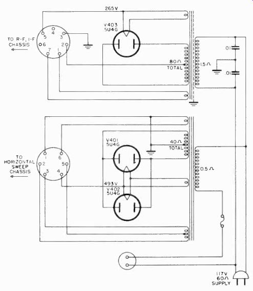
Figure 57. Low voltage power supply.
The output tubes are coupled to the deflection coil through T302. L302 is provided to vary the output and hence the picture width by shunting a portion of the T302 secondary winding.
The horizontal size is also affected by R340 which varies the amount of negative pulse added to the sawtooth voltage that is applied to the grid of the output tubes. The negative pulse is added to the sawtooth by feeding back a portion of the pulse from the secondary of the output transformer. The size of this pulse, which is controlled by R340, affects the point at which the output tubes conduct. This in turn determines the amount of deflection current fed to the yoke, and hence the horizontal size. Clockwise rotation of the control increases the picture width, crowds the right side of the picture, and stretches the left side.
The horizontal linearity control R351 changes the time constant of the differentiation network in the 6AS7G (V310) grid circuit and determines the portion of the trace over which this tube conducts, thus controlling linearity on the left side of the picture. Counterclockwise rotation of the control causes the left side of the picture to stretch. R340 and R351 are adjusted together to set the horizontal size and linearity.
7-48 Low Voltage Power Supply. The low voltage power supply chassis contains two separate power supplies. One supply provides the filament and plate voltages for the RF/ IF chassis, and the other supply provides for voltages for the horizontal deflection circuits. This latter supply employs an interlock cable to the horizontal deflection chassis and a fuse in the power transformer primary to protect the supply in case of short circuits in the horizontal deflection chassis. The supplies employ conventional full wave rectifier circuits. A single 5U4G, V403 (Figure 57), is adequate to furnish the current for the RF/ IF chassis. L117, C173A, C166A, and C172A (Figure 53) provide filtering of the B+ supply. The center of the transformer secondary is grounded through a bleeder consisting of R188A, R187A, R180. Negative voltage is obtained across this bleeder for the positioning circuits and bias voltages on the RF/ IF chassis.
7-49 High Voltage Power Supply. The high voltage power supply which feeds the intensifier of the projection tube is of the kickback type. It is located on the horizontal deflection chassis, and its circuit is shown in Figure 56. When the 6BG6 plate currents are cut off during the flyback time of the horizontal sawtooth voltage, a positive pulse appears on the T302 primary due to the collapsing field in the deflection coil. This pulse of voltage is stepped up by the autotransformer action of T302 and is applied to the plate of the high voltage rectifiers.
Three type 8016 tubes are employed in a voltage trippler circuit which produces approximately 27 kv dc for operation of the projection tube. The pulses are first rectified by V307 and charge capacitor C326 to near peak voltage. Since the cathode of V307 is connected to the plate of V308 by resistors R342 and R343, capacitor C327 will charge to the same voltage as C326.
The charge on C327 is thus added to the incoming pulse, and V308 rectifies the sum of these voltages, thus charging C328 to double the pulse voltage. The cathode of V308 is connected to the plate of V309 through R344 and R345, charging C329 to the same voltage as C328. The charge on C329 is added to the incoming pulse. V309 rectifies the incoming pulse and the d-c charge on C329 to charge C330 to three times the pulse voltage. The initial pulse voltage is about 9 kv, so that approximately 27 kv are obtained at the output of the voltage trippler.
Since the frequency of the supply voltage is high (15,750 cps), relatively little filter capacity is necessary. C330, a 500-mmf capacitor, and the capacitance of the lead to the projection tube are all that are required. A bleeder consisting of R329 through R333 is connected across the first rectifier stage to provide the 4-5 kv for the focus electrode of the electrostatically focused 5TP4.
7-50 Audio Circuits. A portion of the energy absorbed by the trap T2 is fed to the first sound IF amplifier V101, shown in Figure 53. Three stages of amplification V101, V102, and V103 are used to provide adequate sensitivity. A conventional discriminator, V104, is used to demodulate the signal. The discriminator band width is approximately 350 khz between peaks.
This wide frequency response allows for some drift of the oscillator in the RF tuner, for normally only a 50 khz pass band is needed for the television sound. The output from the discriminator is fed into the radio audio system and is controlled by the radio volume and tone control.
The AM/ FM receiver in the 648PTK is comprised of an eight tube AM/ FM tuner unit and a four tube audio amplifier and power supply. The tuner unit employs an RF amplifier on all bands. One 455 khz IF stage and a conventional diode detector are employed on AM. On the FM band, three 10.7 Mhz IF stages and a ratio detector are employed. These circuits are entirely independent of the video sections of the receiver.