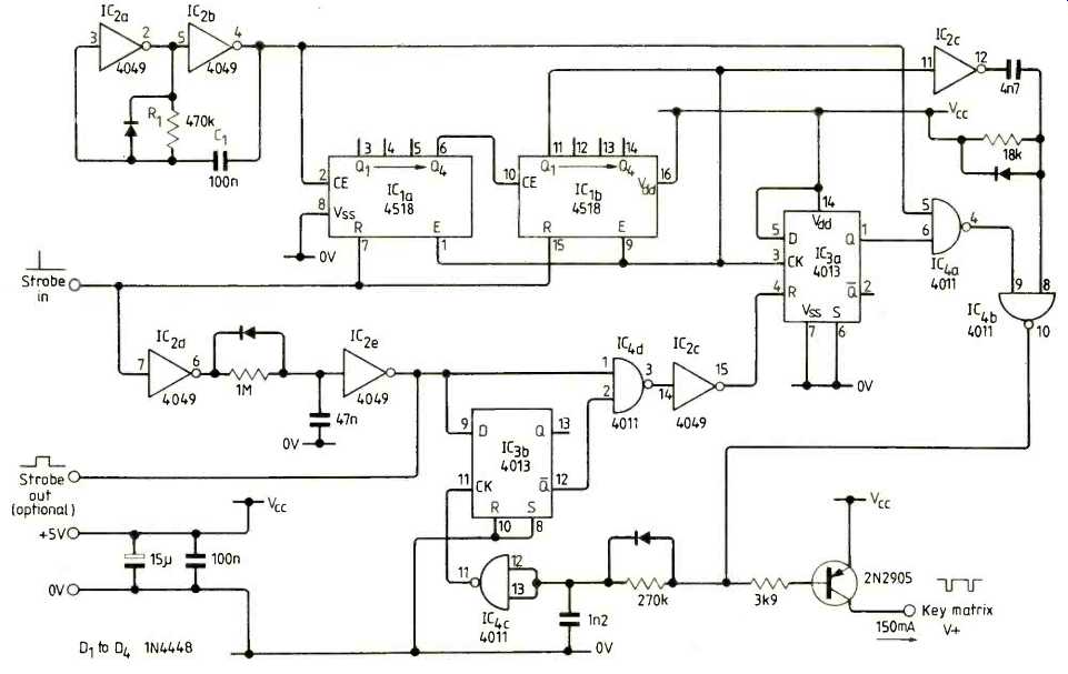
Auto repeat for Hall-effect keys
Surplus Hall-effect keyboards can be obtained cheaply, but they often lack a repeat key or auto-repeat function. Many Hall-effect keys produce a single pulse when pressed, as opposed to a continuous output, and so do not lend themselves to this function. This design provides delayed auto-repeat on such keyboards and requires only three connections to the existing circuit.
The key matrix of a Hall effect keyboard is powered by a d.c. source, usually +5V or +12V. The pulse produced by pressing a key is translated into an Ascii value and a strobe pulse by the keyboard controller.
This additional circuit switches the power supply to the matrix so that while a key is pressed, a pulse is produced each time that the supply goes from low to high, resulting in multiple strobe pulses. Supply to the controller is continuous of course.
Auto repeat at 10Hz starts about is after pressing a key.
Repeat frequency is determined by R1/C1 and delay period by the 4518 dividers; both are adjustable. The only connections between this and the existing circuit are the strobe pulse, power supply and key-matrix supply driver. Keys on which auto-repeat is not required may be connected to the continuous supply.
An extended strobe pulse is available. This is for use in terminals or computers using keyboard polling where the normal strobe pulse may be too short. All i.cs are cmos so adaptation for other supply voltages is easy. Note that the transistor is not intended to switch large capacitive loads, so make sure that there are no large decoupling capacitors in the key-matrix supply circuit.
In steady state or after power up, IC3a is reset and IC pin six is low. Pins eight and nine of IC4b are both high so the transistor is saturated and a continuous current flows through the key matrix.
Pressing a key produces a positive strobe pulse at the input and resets both counters, IC1a,b. After this narrow pulse, both counters count up to 20, output Q1 of IC1b becomes high and the counter stops.
The counter output low-to-high transition generates a pulse to drive the transistor base and clock input of IC3b.
The transistor opens for a short time, producing one pulse in the matrix. If at this point the key is still pressed, a new strobe pulse occurs and restarts the counters; this pulse is stretched to around 10ms by the circuit around IC2d,c. This strobe pulse is fed to the D input of a bistable device, IC3b Clock input of this device is triggered by the delayed matrix pulse through IC4c, IC3b is set and the reset condition of IC3a is removed through IC4d and IC2f. At the next counter time-out, IC3a is set and asymmetrical clock pulses from IC2 are sent through IC b to the transistor.
The matrix is now switched at the clock rate until the key is released. After release, the strobe pulses disappear, IC3b is reset and the circuit returns to its steady state.
---------------
Asynchronous data separator for modems
*Electronic Engineering Association, Leicester House, 8 Leicester Street, London WC2H 7BN.
An economical solution is shown for the asynchronous data separator requirement in modems having a three-to-two frequency ratio.
Timings shown relate to a standard recommended by the EEA* for data transmission over radio systems. At 1200 baud, a logical one is defined as one cycle of 1200Hz and a logical zero as one and a half cycles of 1800Hz, transmitted with phase continuity, Fig. 1.
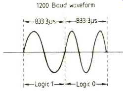
Fig.1. Data format
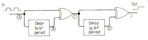
Fig.2. Separator
The signaling rate may also be 600 baud, when a logical one is two cycles of 1200Hz and a logical zero three cycles of 1800Hz.
The system is a synchronous one in that the receiver must be brought into synchronism with the transmitter in order to retrieve the data with the least chance of errors. Since it is necessary to derive the bit rate from the data transitions themselves, a means of asynchronous data separation must be used first, Fig.2.
Received tones are limited to provide a square wave sequence with zero crossings corresponding to those of the input waveform. The sequence is then delayed by one and a half bit periods at 1200 baud and exclusive or'd with itself.
This process is then repeated, but with a delay of one sixth of a bit period, to provide the retrieved data, as shown in the timing diagram. No modification is required for 600 baud operation. The bit pattern used in the example is 110011 at 1200 baud or 101 at 600 baud.
The practical example shown uses a 4731 quad 64-bit shift register as the delay element.
Three of the registers are connected in tandem to provide the half bit-period delay.
Dividing a 3.6864MHz crystal oscillator by eight conveniently provides the 460.8kHz clock.
Since the delay is achieved by a sampling method, a one-bit uncertainty on the 460.8kHz clock exists in the delay value.
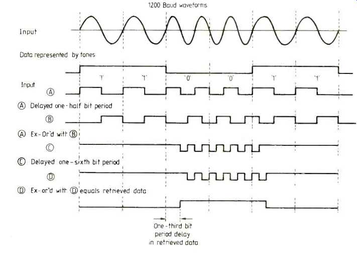
Fig. 3. Timing diagram
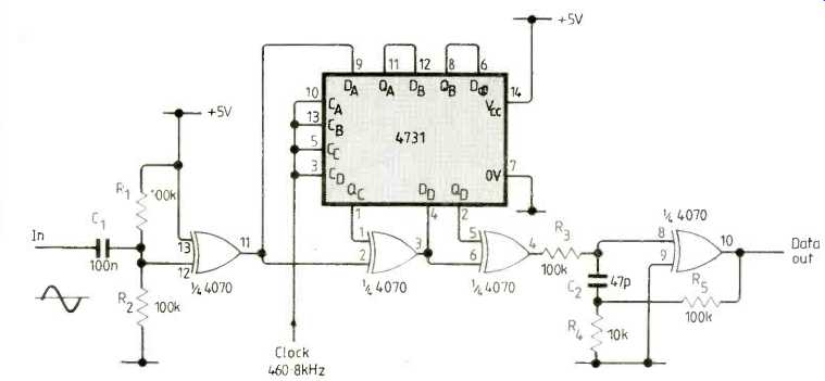
Fig. 4. Practical implementation
This takes the form of glitches varying in width between zero and two microseconds at the output. These are removed by RC filtering at the output gate.
-----------------
Digital distorter
While working on a digital sound processing system, I hit upon the idea of using an eprom to distort the waveform coming into the system. Distortion can vary from simple clipping, which simulates an overdrive pedal, to as complex a nonlinear function as required.
In my system, two eproms provide 16-bit resolution and 16 transfer functions are stored including linear, which has no effect on the signal, and full wave rectify which doubles the frequency of a sinewave input. This circuit is an 8-bit version for simplicity and cheapness. One of 16 functions is selected using four switches.
Capacitors C1 and C2 are chosen to give the required sample rate and conversion times respectively. Input and output low-pass filters are essential and it is also useful to be able to adjust input gain for the best s/n ratio.
----------------
Vectored interrupts on 68 series processors
There is only one IRQ interrupt-request address for all peripherals on 68xx-series microprocessors but eight or more are possible using continuous scanning under control of the processor E clock. When an interrupt signal is detected, it is latched and the counter holds a value corresponding to the interrupting peripheral. The counter content is used by the processor as part of the service address for its interrupt-service routine; note that address line A, is changed to zero. This gives a pair of bytes to each peripheral in the range FFE0 to FFFF_16.
The number of peripherals can be increased to 16 by an extra 74LS150 and gates to make A5 zero when the IRQ service occurs. On the 6809, a dual system can be implemented for IRQ and FIRQ.
==========
(adapted from: Wireless World , Apr. 1985)