Current mirrors and a conventional opamp combine to form an accurate current follower. Its advantages are illustrated in a universal voltage amplifier design exhibiting high gain, bandwidth and stability.
by F.J. Lidgey Ph.D., B.Sc., M.I.E.E. and C. Toumazou B.Sc.
==========
Christofer Toumazou completed an OND in Technology in 1980 from North Gloucestershire College of Technology. He then joined Oxford Polytechnic obtaining a first class honors BSc in Engineering in 1983. Currently he is studying for an M.Phil/Ph.D on opamp circuit design, supervised by the co-author of this article. His research program also includes part-time lecturing at the Polytechnic.
John Lidgey is Principal Lecturer in electronics at Oxford Polytechnic. His teaching and research are both in the area of analogue circuit design and applications. In addition he is actively engaged in industrial electronics consultancy.
==========
This current-follower circuit uses a conventional operational amplifier and two current mirrors. We analyze the circuit to show its most-significant characteristics, and a prototype is shown to perform well in practice. Using this circuit together with two voltage followers we have constructed a universal voltage amplifier. Theoretically, this universal amplifier structure is extremely stable and exhibits high gain and bandwidth simultaneously; experimentation has shown this to be true.
A current follower is the antithesis of a voltage-follower. The ideal current follower has zero input impedance, infinite output impedance and unity current gain. The circuit is effectively a current-buffer enabling the maximum available current to be transferred from a signal source and fed into a nonzero-impedance load. This application together with others has been discussed by Nordholt' and Lidgey [2].
In this article a simple current follower circuit is developed using a conventional opamp and current-mirror circuits. The current-follower produced is then employed in a universal amplifier as described in the second reference. This amplifier uses only voltage and current-follower circuits together with resistors to define the closed-loop gain. The performance of such an amplifier is extremely good. The bandwidth is wide and it is not inversely related to the closed loop gain, and no stability problems exist as there is no direct feedback from output to input.
Improved current-follower circuit
In order to appreciate the final design, it is worthwhile considering the simple current-follower circuit, Fig. 1. One end of the load is held close to zero volts by feedback action of the opamp, however the load is essentially floating as neither side may be connected directly to ground.
Despite this drawback, the circuit does have some interesting features. Input impedance is extremely low as nearly all the input current is drawn through the load by the action of negative feedback. Input current only differs from the load current by the current flowing into the opamp which is extremely small due to the high open-loop voltage gain and input impedance of the op amp.
Most applications require a circuit able to feed a grounded load and so a modified version of Fig.1 is needed, Fig. 2. The feedback path from the inverting input to the opamp output is now a short circuit which further reduces the input impedance compared with the circuit of Fig.1.
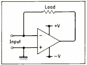
Fig. 1. Simple current follower circuit. Although one end of the load is held
close to zero volts by feedback action, the load is essentially floating and
may not be grounded.
As before, input current is drawn around the feedback path by the opamp. Positive input current flows in a path around the feedback loop into the opamp output and through to the supply lead of the opamp to the negative power supply. Widlar's current mirror current-sink' is used to sense this supply lead current via the diode connected transistor Tr, and then reflect this current in Tr4 to the load. Similarly negative input current results in an equal positive supply current which is reflected into the load by a p-n-p current-mirror current source comprising transistors Tr [1, 3].
The circuit is essentially that of an opamp configured as a trans resistance stage, the output of which is taken through the power supply leads. As the opamp is directly coupled, the output effectively phase splits and the two complementary current mirror source and sink circuits recombine the split phases into a ground connected load.
Accuracy of the current following action is limited by the current mirror performance. As discussed by Lidgey4 the ratio of image to reflected current, K, in the simple Widlar type of current mirror is given by
K =Beta/(Beta+2) (1)
Clearly an accuracy of 2% will result if the current gain, of the mirror transistors is 100. This is not regarded as acceptable and the improved current-mirror developed and analyzed by Wilsons is used to replace the two Widlar type current mirrors.
Figure 3 shows the final current follower circuit design using these improved current mirror circuits.
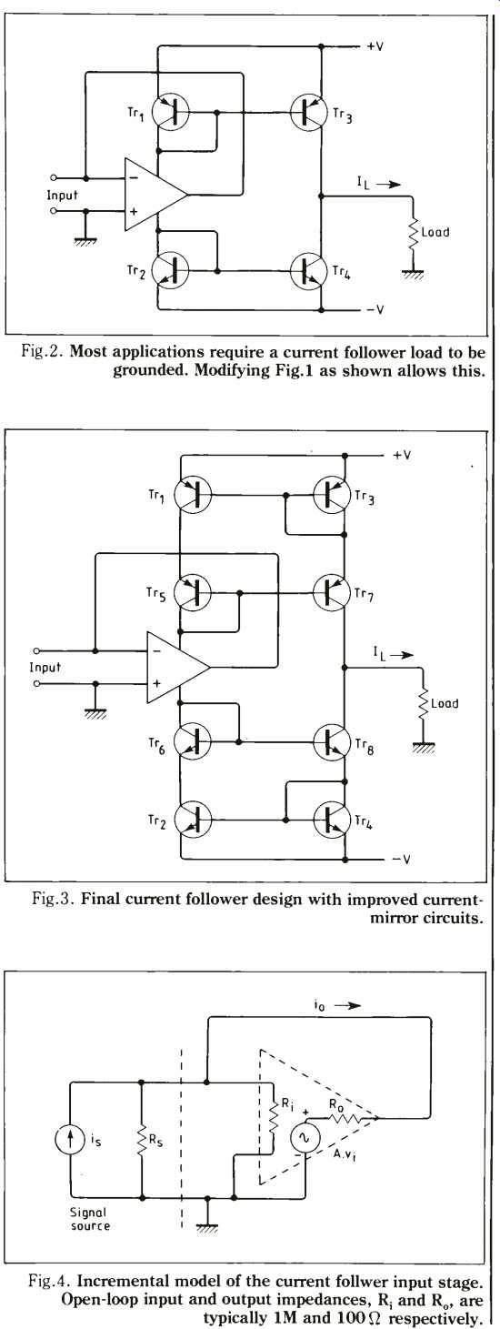
Fig. 2. Most applications require a current follower load to be grounded.
Modifying Fig.1 as shown allows this.
Fig. 3. Final current follower design with improved current mirror circuits.
Fig. 4. Incremental model of the current follower input stage. Open-loop input and output impedances, R1 and R0, are typically 1M and 100 ohm, respectively.
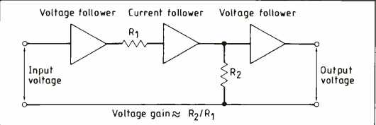
Fig. 5. Universal voltage amplifier using 741 opamps and current mirrors constructed
from bipolar transistor arrays.
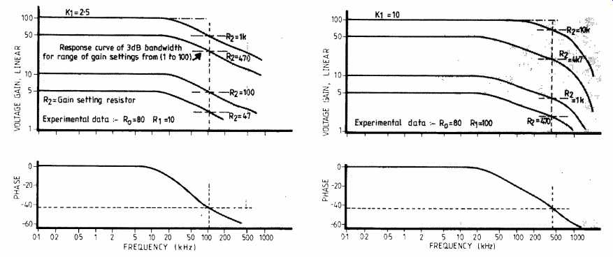
Fig. 6. Frequency response of the voltage amplifier for K1=2.5 (a) and K1=10
(b).
Follower analysis
The incremental model of the op amp is shown in Fig.4. Resistance R1, typically 1M-ohm or so, is the open-loop input impedance and Ro, typically 100 ohm or so, is the open-loop output impedance.
The dependent voltage generator, A. vi represents the high open-loop differential voltage gain of the opamp, where A is of the form
A = Ao/(1+jf/fp) (2)
Factor Ao is typically 10^5 or so and is the d.c. open-loop voltage gain of the opamp. Frequency 4, the upper-3dB cut-off frequency, is typically 10Hz or so. This upper cut-off is introduced by the manufacturer through an internal on-chip frequency compensation network to ensure that the op amp will not oscillate when used with any value of resistive negative feedback.
Analysis of the circuit yields the current transfer ratio io /is of
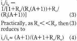
Clearly from (4) the current transfer ratio is close to unity for high values of A. Solving for the small-signal input impedance Z; gives the following equation
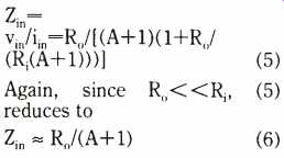
It is interesting to note that load resistance RL is effectively isolated from the opamp output and as a result the effect of changing the load has negligible influence on the closed-loop performance of the opamp. Furthermore compared with Lidgey's follower circuit which gave an input impedance of
Z;=(R+RL)/(A+1) (7)
the follower described here has a lower and therefore more ideal value of input impedance.
Consider now the frequency response of the follower. Substituting for A into (4) using (2) and so obtaining the frequency response of the current transfer ratio, then
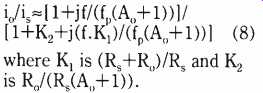
Substituting the symbol GB for the gain-bandwidth product of the opamp, which is equal to ff(A+1), and neglecting KZ as generally Ao>>Ro/R5, then (8) reduces to,
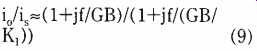
To a first order approximation one may assume that the frequency response of the current mirror section of the circuit is much higher than the remainder and so the frequency response of the follower, dominated by the opamp section, is given by
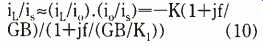
where K is the mirror performance ratio of reflected to image current.
Equation (10) demonstrates that the bandwidth of the follower is essentially independent of the load impedance used.
General purpose voltage amplifier
Any of the four basic amplifier configurations may be constructed using up to two voltage followers and up to two current followers as described by Lidgey. The circuit of Fig. 5 is a voltage amplifier built using two voltage followers cascaded with a central current follower. Resistors R1 and R2 define the voltage gain,
Av = R2/R1 (11)
assuming that each of the three followers has precise unity gain.
A prototype circuit of Fig.5 was built using 741 opamps and current mirrors constructed from two bipolar transistor arrays, these being a 2N3046 and a CA3096. It is essential to use single-chip well matched transistors for current mirror circuits4.
Frequency response of the prototype is shown in Figs. 6a, b for two different values of K1, the voltage gain being set by R2.
One can see from the experimental results that the bandwidth does not alter when R2 is changed to give different values of voltage gain. It is interesting to note that the conflict between gain and bandwidth generally encountered with more conventional designs using internally compensated op amps, does not occur with this structure of amplifier.
Bandwidth of the voltage followers is approximately 1MHz and the frequency response of the circuit is limited mainly by the current follower. Increasing R1 results in a reduction of K1 and hence an increased frequency response of the current follower circuit, as indicated by equation (9). Although bandwidth will tend to increase by increasing R1, to maintain a fixed voltage gain R2 must be increased in proportion.
However there is a limitation on the size of R2 and hence the voltage gain possible due to the finite output impedance of the current follower; measured at 10kHz to be 3M-ohm..
References
1. Nordholt, E.H., Extending Opamp capabilities by using current-source power systems, supply, IEEE Trans. CAS-29, No 6, June 1982, 1t and spp.411- 414.
2. Lidgey, F.J., Current Followers, Electronics and Wireless World, February 1984, pp.40-43.
3. Widlar, RJ., Some circuit design techniques for linear integrated circuits, IEEE Trans. Circuit Theory, Vol.CT-12, December 1965, pp.586-590.
4. Lidgey, F.J., Looking into Current Mirrors, Wireless World, October 1979, pp.57-58.
5. Wilson B., Current Mirrors, Amplifiers and Dumpers, Wireless World, Vol. 78, No. 1551, December 1981, pp. 47-50.
==========
(adapted from: Wireless World , Apr. 1985)