Besides new instructions, the 68020 has additional hardware features- cache memory, dynamic bus sizing and pipeling.
by DAVID BURNS and DAVID JONES
Adding a coprocessor enhances the main general purpose processor by incorporating new instructions, registers and data types into the system without overloading the main processor.
Interfacing between the main processor and coprocessor is not noticed by the user i.e. the programmer need not be aware that a separate piece of hardware is executing some of the program-code sequence. In the 68020 microcode within the device takes care of coprocessor interfacing so that any co processors appear as a natural extension to the main processor architecture.
Using devices without a coprocessor inter face such as the 68008, 68000, 68010 and 68012, communication between the main c.p.u. and coprocessor is possible by observing the correct sequence of coprocessor primitives necessary for the interface. These primitives are a method of passing commands and data between the main processor and coprocessor.
Accessing coprocessors over the co processor interface is straightforward since the interface is implemented using standard M68000 asynchronous bus structure with out the need for any special signals. This not only makes the interface simple; because of the asynchronous nature, the main processor and coprocessor can be operating at different clock frequencies. Designers can therefore optimize a system to make best use of the speed options available.
The coprocessor need not be architecturally similar to the main processor but can be designed so that it best suits its required application. The only requirement is that it adheres to the coprocessor interface protocol. A coprocessor can indeed be implemented as a v.l.s.i. device, as a separate board or even as a separate computer.
When communicating with a coprocessor the MC68020 executes bus cycles in c.p.u. space to access a set of interface registers (cm). The 68020 indicates that it is accessing c.p.u. space by encoding the function-code lines as all high (Fc0_2 =1112). Chip selection of the coprocessor and the relevant register is then performed by the address bus.
Encoding of the address bus during coprocessor communication is shown in Fig. 1a.
This illustration shows that by using the operand data and effective addresses.
'Cp-ID' field on the address bus up to eight separate coprocessors can be interfaced con currently to the MC68020. Figure lb shows how simply this can be done.
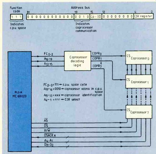
Fig. 1. Address bus coding during coprocessor communication (a) and
an illustration of how up to eight coprocessors can be connected (b)
using the Cp ID field.
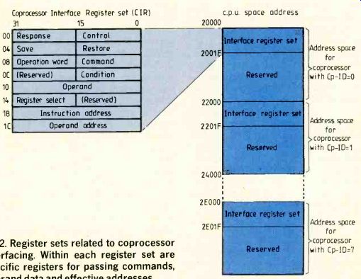
Fig. 2. Register sets related to coprocessor interfacing. Within each
register set are specific registers for passing commands.
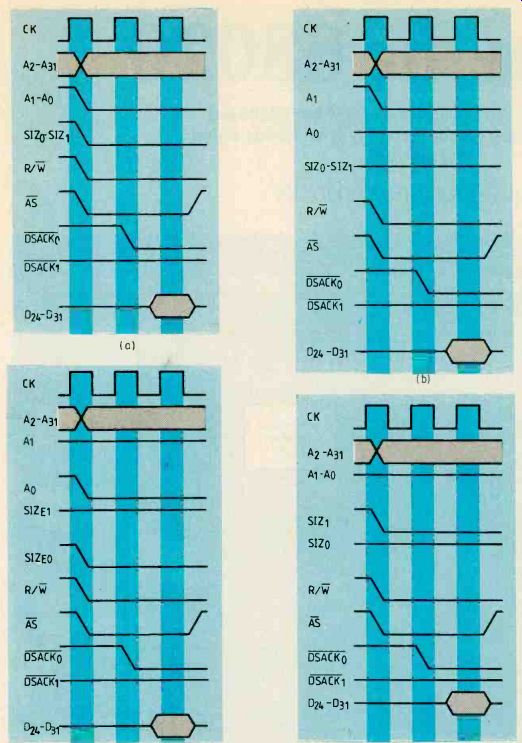
Fig.3. Timing of the four cycles required to write a long word into
an eight-bit memory. In all four diagrams, DSACK0 is zero and DSAcK1
is one, indicating that the memory is eight bits wide. At (a), signals
size 1 are both low to indicate that the processor has four bytes to
transfer and the states of these two signals change from 1,1 to 0,1 to
1,0 in (b), (c) and (d) to indicate three, two and one bytes to transfer
respectively.
You can see that, if required, there could be several 68881 floating point coprocessors operating concurrently in your system to facilitate very fast and complex number crunching. Interfacing to these separate coprocessors is simply a matter of encoding the relevant Cp-ID in the coprocessor instruction, and hence on the c.p.u. space address-bus encoding, so that the MC68020 will communicate with the relevant register set in c.p.u. space.
Figure 2 shows how the separate interface register sets are located in c.p.u. space.
Within this interface register set the various registers are allocated to specific functions required for operating the coprocessor inter face. There are registers specifically for passing information such as commands, operand data and calculated effective addresses (effective address calculations, and associated operand fetches, are performed by the main processor). Other registers are allocated for use during a context switch when the internal state of the coprocessor needs to be saved and then restored.
DYNAMIC BUS SIZING
The 68020 can dynamically change the size of the data bus on each bus cycle. This feature has been included so that the processor can communicate with peripheral devices intended for 32, 16 or 8-bit buses.
Dynamic sizing can also be used to retrofit a 68020 in a 16-bit system and although the full performance increase of a 32-bit processor is not gained, performance improvement can be considerable.
Four signals have been added to support dynamic bus sizing, namely DSACK0,1 and siz0,1. Data transfer and device-size acknowledge signals DSACK01 replace the DTACK (data transfer and acknowledge) asynchronous-bus handshaking on the 68000. As with the 68000, these signals are used to terminate the bus cycle but they also indicate the external size of the data bus. Signals siz0,1 are outputs indicating how many bytes are still to be transferred during a given bus cycle.
To illustrate this principle, consider the 68020 writing a long data word (32 bits) to an eight-bit memory device. (This would have a serious effect on system performance as four write cycles would be needed). Bus timing diagram Fig.3 shows the four cycles required to write the information into memory.
Using dynamic bus sizing, during a write cycle the 68020 always drives the entire 32-bit data bus even though all 32 bits may not be used. If data is transferred as a byte, it is placed on 024-31, if it is transferred as a word it is placed on D16-31 and if it is transferred as a long word D0-31 are used.
A multiplexer within the 68020 routes data to various sections of the data bus depending on bus size. Address lines A0,1 are linked to this multiplexer. Their encoding indicates a one, two or three-byte offset for a long word to be read from or written to memory.
Unlike other 68000-family processors, the 68020 allows you to place data misaligned in memory, including the user and supervisor stacks. As far as the programmer is concerned this misalignment goes unnoticed in the hardware but it affects performance by increasing the number of data transfers. In fact the only limitation on data storage in the 68020 is that the instruction word, or op-code, must lie on a word or long-word boundary. This is to retain upward software compatibility with 68000-family software.
Consider this example illustrating the principle of misaligned data transfers. Data is transferred to memory by the 68020 over a 32-bit data bus, however the memory address has been offset by one byte from a long-word location.
Figure 4, in which the timing diagrams are simplified to show just the signals used to control data flow, clarifies the situation.
Tables summarize decoding of the size and DSACK signals. Also shown is a representation of how the data is organized within the processor.
Since the data is misaligned by one byte the processor needs to make two memory accesses to transfer the long word. During the first cycle, three bytes of data are transferred and the second cycle transfers the last byte.
During the first transfer the processor sets the size pins low to tell the memory that the processor has four data bytes to transfer (a long word). The memory address is odd and offset by one byte from a long-word address so address lines A0,1 are at logic one and zero respectively.
Using DSZK0,1, the memory controller indicates that it is 32 bits wide. Information placed on the data bus, in long-word form displaced by eight bits, is carried on 023-0.
The lower eight bits are not transferred during this cycle. Information placed on D31_24 is just a mirror image of data on D2S_16 and should be ignored by the controller during a write cycle.
During the second transfer, the long-word transfer is completed. Again, DsncK0,1 indicate a 32-bit port but the size pins indicate to the memory controller that only one byte remains to be transferred. Data is transfer red as one byte on address/data lines 024.31.
Inside the processor, data is transferred within the registers on the opposite end of the data bus. The remainder of the data bus carries a mirror image of this data and should be ignored during write cycles to memory.
Figure 5 shows data transfers over a 16-bit port misaligned by one byte. In this example, it takes three data transfers to transfer a long word. These examples illustrate that the 68020 can be designed into systems with 32, 16 or indeed 8-bit data buses and with a large possibility of data being placed in aligned and misaligned memory.
CACHE MEMORY
Increasing the speed of the 68020 from 16.7MHz to 20 and 25MHz has been accompanied by increases in the cost and difficulty of interfacing the device to external memory without using wait states. The device's internal 256-byte instruction cache relieves this problem.
A minimum of three clock cycles is required when the processor accesses external memory. However if the information is held in the cache, which can be thought of as very fast on-chip local memory, then only two clock cycles are required.
Computer simulation tests were carried out for the 68020 based on the 68000 architecture to find out what type and size of cache would be most beneficial; 256 bytes was found to be the best compromise between efficiency and cost. The cache theory rightly assumes that modern computer programming involves the program repeatedly executing small sections of code as opposed to randomly jumping over large linear address spaces.
When the processor fetches an instruction from memory, the processor is redundant since no processing can be performed until the instruction has been decoded (this is not strictly true for the 68020). If this instruction fetch can be performed from the cache then the processor spends less time waiting for information from external memory. This has an even greater effect if there is a memory-management unit (m.m.u.), external bus or magnetic backup storage in the system. In such cases it may not always be possible to access external memory with no wait states.
The cache, Fig. 6, is 'hit' when address field A8-31 and function-code Fc2 (indicating instruction accesses) match the international cache tag field. Cache hit is a term used to describe the condition where the address and any other control information presented on the bus matches information previously placed in the cache tag field.
Some 64 long words are available for storage of cache information. Since the cache is always updated on a long word, maximum throughput is achieved when two instructions in memory are held in the cache. Address lines A2.7 select one of 64 entries, upon reset, the cache is disabled and all entries are made invalid; the y bit in the tag field is also cleared.
Two registers are used with the cache-the cache-control register, CACR, and the cache address register, CACR. Enabling, disabling and clearing of the cache is carried out by the control register. This register can also be used to freeze individual entries in the cache so critical code sequences can be run within the cache.
It is not possible for the programmer to access cache entries directly. Programming the cache registers is performed using the MOVEC instruction and so can only be done in supervisor mode. This ensures that the user cannot accidentally effect the cache operation. Using cache clearing, the operating system can perform a fast context switch in just one instruction.
In addition to the software cache-enable facility, an external hardware cache disable pin, CDIS, can be used to dynamically disable the cache on the next internal cache-access boundary.
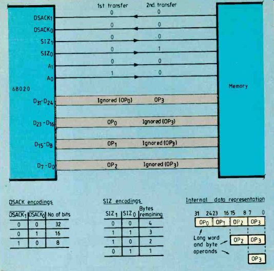
Fig. 4. To send data to memory over a 32-bit address bus when the memory
address is offset by one byte from a long-word location requires two
transfers. The operand is 32 bits and the boundary is one byte.
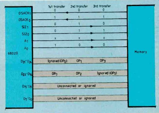
Fig. 5. To transfer a long word over a 16-bit port misaligned by one
byte takes three transactions. The operand is 32 bits and the boundary
odd. Data lines 00.15 are either unconnected or ignored by both the processor
and memory on 16-bit port-sized transfers.
THE PIPELINE
Within the 68020 is a three-stage pipeline used for instruction execution, Fig.7. Instructions enter the pipe either from the external bus or from the instruction cache, also within the processor. These instructions are not the ones currently being executed but are 'prefetched' instructions obtained by the bus-interface unit.
With pre-fetching, long words are always fetched and the cache is arranged as long words. After a prefetch has been requested, the long-word obtained is placed in a 32-bit holding register (stage A) called the cache holding register. This register is used to hold the prefetched long word in the case of a cache miss or to hold the pre-fetched long word from the cache if a hit occurs.
When a cache hit occurs, the external bus performs an aborted cycle with the ecs pin asserted followed by a second assertion of ECS. Address-strobe pin AS is not asserted during a cache hit. If data is prefetched from the external data bus, it is routed directly to the 32-bit arithmetic logic unit, or a.l.u.
This a.l.u., with which is associated a 32-bit barrel shift register, performs arithmetic and logical operations on data registers.
From the cache holding register, instructions pass to stages B, C, and D, where the instruction is executed. Movement through the pipe is governed by the execution time of the instruction at stage D. On reaching stage D of the pipe, the executing instruction corresponds to the program counter.
However the processor needs to know where the extension words, etc, for the instruction are so temporary pointers are set up for each stage of the pipe and holding register. These pointers are used to obtain data from each stage of the pipe to allow completion of the instruction.
Using pipeline architecture, the processor operates much faster since no external bus cycles are needed to fetch extension words, etc. Flow of the temporary pointers is tracked by a 32-bit arithmetic unit. There is a third arithmetic unit in the 68020 for arithmetic operations between address registers such as calculating effective addresses. To produce effective addresses needed by the instruction when it is in stage D of the pipe, stage c can be used for effective address calculation. Stages c and D have inputs for allowing them to control the 32-bit a.l.u’s and a.u’s.
David Burns graduated with an Honors degree in Electronic and Microprocessor Engineering from Strathcylde University in 1983. Since then he has worked for Motorola Semiconductors in East Kilbride. Presently David is working as a 16/32 bit Applications Engineer and has just completed work on a 25MHz high performance MC68020 computer board.
David's hobbies include orienteering, tennis and badminton.
David Jones graduated with an honors degree in Electronic Engineering at Heriot Watt university in 1982. Since then he has worked for Motorola Semiconductors in East Kilbride. After working as an equipment engineer David transferred to the microprocessor applications group, progressing from eight to 16 to 32 bit processor design. He is currently working on a 25MHz high performance MC68020 computer board.
David's hobbies include white-water canoeing (both recreational and competitive), swimming and car maintenance. He enjoys outdoor life.
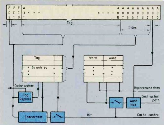
Fig.6. Accessing external memory slows down processing so the 68020
processor has a 256-byte internal cache memory to reduce this problem.
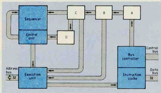
Fig.7. Within the 68020 is a three-stage pipeline which reduces execution
time since external bus cycles are not needed to fetch instruction extension
words, etc. Instructions enter the pipe either from the external bus
or from the instruction cache.
============
MASTER/INTERRUPT STACKS
Most high-performance microprocessors have two stack pointers. One is usually to the system stack, reserved for interrupts, etc., and the other is the user stack for temporary data storage and parameter passing. In the 68020, these stacks are A7 and A7.
During normal operation most code will be executed in user space and programs will use the A7 stack for temporary data storage and parameter passing between software routines. Interrupt stack A7' will only come into use when an exception occurs, such as an external interrupt when control is passed to supervisor mode and the relevant exception processing performed.
In many microprocessors this supervisor stack pointer is the only one accessible during exception processing and all data storage and context switching has to be performed on only one stack. With complex multi-tasking maintaining the main system stack costs processing time; interrupt information for the program counter and status register is interleaved with process-control blocks for various software tasks.
This problem is alleviated in the 68020 by a third stack- the master stack- specifically for holding process-related information for the various tasks. When the master stack is enabled, through bit M in the status register, all non-interrupting exceptions like divide-by-zero, software traps and privilege violation are placed in the user's process-control block on the master stack.
When the first interruption occurs, typically a timer interrupt from a preemptive scheduler, the processor places the program counter, Pc, the status register, SR, and the vector offset on the master stack A7. It then duplicates this information on the interrupt stack A7. The processor is now free to manipulate the processor control block without any further interrupt information being placed on the master stack.
All subsequent interrupts received while performing exception processing are placed only on the interrupt stack A7. An effective context switch can now be performing by simply reloading the master stack pointer and mapping in another task's process-control block. This allows context switching to be performed without any master-stack modification by higher-priority interrupts which may occur during the exception processing for the preemptive scheduler's timer interrupt.
=========
Also see:
=========
(adapted from: Wireless World , Jan. 1987)