32-BIT COMPUTER
Computer boards accessing memory across a non-standard bus designed to suit the microprocessor have advantages over systems using industry-standard buses, according to a note on National Semiconductor ICM332-1 integrated computer modules.
These advantages are that price decreases because there is no need for backplanes and card cages, and performance increases be cause all memory is accessed through a local bus tailored to suit the processor.
Boards described in the note are based on 32-bit Series 32000 processors and peripherals which include the NS32332 c.p.u., 32201 timing controller, 32082 memory manager, 32081 floating-point unit and 32202 interrupt-control unit. These modules are intended for designing into office automation, workstation, graphics and process-control equipment.
The c.p.u. board has 2M-byte of ram with parity checking but can access a further
12M-byte through its 32-bit Maxibus. Further boards provide i/o processing, with s.c.s.i., and memory expansion. National's Unix operating-system port Genix V3 is available for use with the boards.
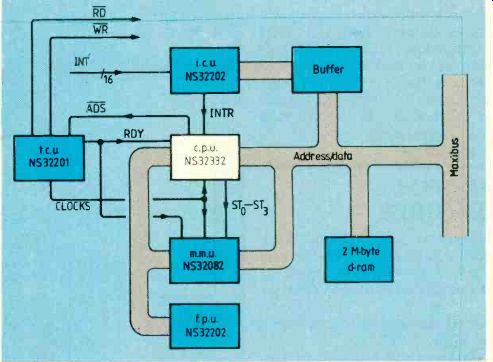
IMAGE SENSING D-RAM
When light falls on a dynamic memory cell its storage capacitor discharges at a rate proportional light intensity and exposure duration. It has been known for some time that with certain types of d-ram, if you can successfully expose the top part of the chip, you can use it as a crude image sensor.
Now an American company is manufacturing specially fabricated dynamic rams with a glass window on top for image sensing.
Unlike ordinary d-rams, these devices can be adjusted for sensitivity by varying voltage on an analog input pin (pin 1 for the d-ram pinout experts).
As with ordinary dynamic rams though, these i.c’s have two or more separate memory matrices on the chip depending on the version. With the 64K-bit device there are two 128-by-256 element matrices for example so a picture sensed using the whole chip has a dead zone either along or down the middle. But the sensors are intended for computerized image sensing, in say robotics applications and process control, so the dead zone becomes less of a problem. Of course just one matrix can produce a lower resolution picture without a dead zone.
In order to achieve high chip density, cells within the chip are staggered so the address matrix does not correspond exactly with the physical matrix. Unless the image representation is rearranged, either in hardware or software, it will lack definition because of the staggering.
There are two possible ways of achieving a grey scale, one by varying the threshold voltage and the second by altering the scan rate. Although varying the threshold voltage seems most obvious, the manufacturer suggests that altering the scan rate is the best method.
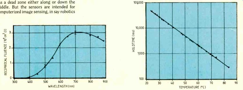
Topology is described in detail in the device data sheets. These graphs come from the IS32 Optic-Ram Spectral data applications note. This note discusses sensitivity, effects of threshold voltage (pin 1), dark current and pixel-to-pixel and chip-to-chip sensitivity. Reciprocal fluence versus wave length illustrated in the first graph shows that peak sensitivity is about 3 x 106cm^2/J between 700 and 800nm. The second graph is of more general interest, showing the maximum hold time for the un-illuminated d-ram against temperature.
Three Optic-Rams are produced by Micron Technology Inc., one with two 128-by-256 image sensing elements, one with four 128-by-512 elements and one with twenty 128-by-256 elements. They are distributed in the UK by Joseph Electronics.
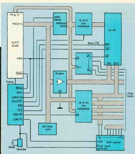
CRT CONTROLLER
Comprehensive design details starting with a comparison between raster and vector graphics are included in Hitachi's 118-page application note for the HD63484 advanced c.r.t. controller. Details of this frame-buffer interface include ram timings and full dot-clocking information. The device's many registers are also explained.
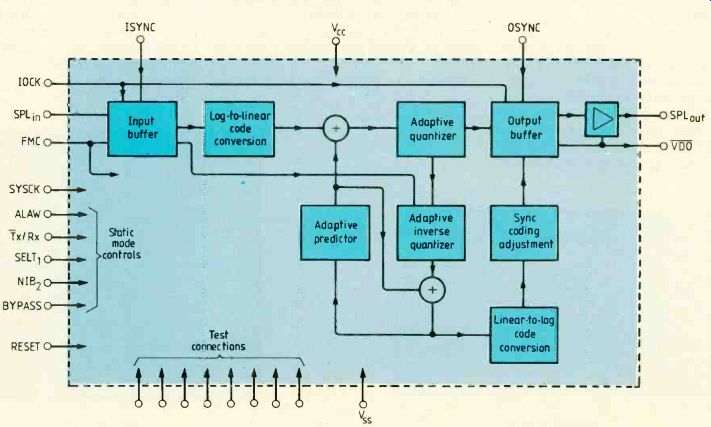
PCM/ADPCM TRANSCODER
Adaptive differential pulse-code modulation, or a.d.p.c.m., increases efficiency in p.c.m. telephone links. The device shown below is a p.c.m./a.d.p.c.m. encoder/decoder called the TEL72.
It has three-state outputs and runs from a single 5V supply.
In conformance with international standards, the c-mos 721 trans-codes 64k-bit/s p.c.m. to 32k-bit/s a.d.p.c.m., or vice versa, on a single speech channel. Switching for either the CCITT G721 or draft UST1Y1 algorithm operation is included and both A-law and µ-law p.c.m. i/o can be handled.
For digital-speech interpolation, the 721 can be operated at lower a.d.p.c.m. rates of 24 or 16k-bit/s.
Several transcoders are shown connected to common input and output buses in the application example. Input in the form of p.c.m. or a.d.p.c.m. is fed to all devices and each device is enabled by a different input strobe so that it responds to only one speech channel. Likewise, each device is enabled by a different output strobe so that it inserts data for one speech channel into the p.c.m. or a.d.p.c.m. output data stream. A nibble selection input assigns the 4-bit a.d.p.c.m. sample to the first or second half of the 8-bit multiplexed time slot.
Currently the 721 complies with G721 1985 recommendations. When pending changes to the C721 and T1Y1 algorithms have been ratified, STC plans to introduce a revised version of the chip.
==========
(adapted from: Wireless World , Jan. 1987)