Discrete-component designs offering up to 500 Vpk output swing, fast stewing and large bandwidth. ‘Modular' approach affords simplicity of design.
By J. BARRON
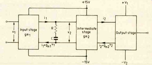
Fig.1. Block diagram of the amplifier. Each stage is considered separately,
the output stage being varied to suit the application.
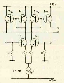
Fig. 2. Circuit of input and intermediate stages. Current mirrors allow
large common-mode signals.
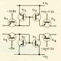
Fig. 3. One version of input to final stage.
Commercially available integrated operational amplifiers are limited to a maximum output of about 80 volts peak to peak, a peak output current of about 25 milliamperes of either polarity, a gain-bandwidth product of about 5MHz and a slew rate of perhaps 50 volts per microsecond.
The output current may usually be increased to the order of 1 ampere by the use of a booster stage, without deterioration of the remaining parameters.
There exist many applications in which outputs exceeding 100 volts and not infrequently output current considerably in excess of 25 milliamperes are required, with a slew rate of several hundred volts per micro second and a large-signal gain-bandwidth product of several megahertz. It is often possible to obtain commercial amplifiers employing thermionic valves to satisfy such requirements, but these are usually expensive.
To design a single amplifier capable of meeting such a wide range of requirements would be a formidable task and, instead of this, a design is suggested in which each stage is unilateral and essentially independent of the following one. This method renders the design of an amplifier to meet a specific requirement systematic and relatively simple. The suggested designs are entirely solid-state though discrete, and offer as economical a solution as is possible within the current state of semiconductor device development.
DESIGN PRINCIPLES
The block diagram of the amplifier is shown in Fig.1. Each stage is designed to be unilateral for all practical purposes, and the output of each of the first two is a high impedance current source, so that each of these stages is characterized by a transconductance and an input admittance. The circuit branch consisting of capacitance C and resistance R in series shown shunting the input of the intermediate stage is a compensating network which will be discussed later. The input and intermediate stages normally require only the 15 volt power supplies which operational amplifiers commonly need.
The output stage is designed to drive the load and may take several forms, dependent upon the performance requirements. It is only this stage which requires high-voltage supplies which are chosen to suit the application, but at the time of writing must satisfy the condition V1+V2<1kV.
Input and intermediate stages. The circuit employed for the input and intermediate stages is shown in essence is Fig.2. In a balanced quiescent state, the achievement of which is assisted by resistors r, each of the six transistors will have an intrinsic trans-conductance gm=20I. The effective trans-conductance of Tri and Tr2 will be modified by the presence of resistance r to gm' =gm/ (1+gmr), so that the greatest voltage gain from an input base to the corresponding collector is -11(1+gmr), whose magnitude is less than unity, Thus the Miller effect at the bases of Tri and Tr2 is reduced.
The admittance seen at the bases of Tri and Tr2 is also decreased by the presence of r.
Since y,'=y/(1+gmr) the effect is to increase r and to decrease C, in the same ratio, so that the input resistance is increased. The intermediate stage is current driven and its bandwidth will be determined by the time constant (C,x'+C,R')/(G+g'), which has been decreased by the presence of r. Thus another effect of r is to increase the bandwidth of the intermediate stage. In designing the overall amplifier circuit, the values of r in the input and intermediate stages are chosen to give the required value of open-loop, low-frequency gain.
A further advantage of the use of current mirrors in the input stage is that it enables a large common mode signal to be accommodated. If the current mirrors employ discrete single, rather than dual transistors, their current ratio may be improved by adding identical resistors in series with each emitter. These resistors should not be of too large a value since they will increase the Miller effect in the emitter coupled pair.
Output stage. One of a variety of circuits may be used for the output stage, depending upon the particular application of the amplifier. The type of device used in this stage is determined by the output voltage and current required by the load. For voltages up to 350 and currents up to several tens of milliamperes, high-voltage video-amplifier bipolar transistors may be employed in the common-base mode, simply to withstand the required voltage, whilst passing current from the intermediate stage to the load.
Where the required voltage exceeds 350 or the current is greater than several tens of milliamperes, power-fets are more suitable because of low current gain in bipolar power transistors, or the lack of p-n-p devices, or both. These may be used either in the same way as the video transistors, or as source followers in order to reduce the standing power dissipation in the amplifier. The output stage may be either single-ended or push-pull, again depending upon the performance required. At the highest voltage rating currently of 1kV. only n-channel fets are available and, if a push-pull system is needed, a type of totem-pole amplifier be comes necessary.
Whatever arrangement of devices is used in directly driving the load, the complete output stage is designed to be current driven by the intermediate stage. The input section of the output stage will usually contain transistors in the common base configuration, at least one of which will serve to translate the d.c. level of an input current to that of one of the high-voltage power-supply lines.
Figure 3 shows a typical version of the input section of the output stage. In this example it is assumed that the intermediate stage uses p-n-p transistors so that its output current may be at the -15V level. One of the intermediate stage collectors connects directly to Tr5, a high-voltage transistor whose function is simply to transmit the current from one output of the intermediate stage of the current mirror formed by Tr6 and Tr7 and thence to Tr8, which is again a high-voltage transistor passing the current to the final driver stage, or in some cases directly to the load. Transistors Tr' to Tr4 perform a similar function for the other output from the intermediate stage. The bias voltage of 1.2V which occurs in three places in Fig.3 is provided to ensure that the output transistor of a current mirror is not saturated.
The simplest form of output stage has the collectors of Tr4 and Tr8 connected together to form the output terminal, the load being connected from this point to ground. This form is suitable for applications in which the current from the intermediate stage is sufficient to drive the load.
A complementary source-follower circuit is shown in Fig.4. In this case the current from the intermediate stage drives the resistor chain, and the source followers provide large currents on demand, enabling heavy loads to be driven.
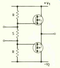
Fig.4. Complementary source follower driven by intermediate stage.
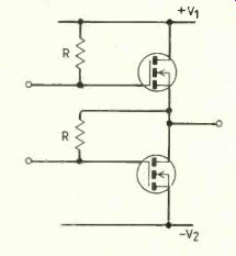
Fig.5. Circuit has similar characteristics to that of Fig. 4, but at
higher voltages.
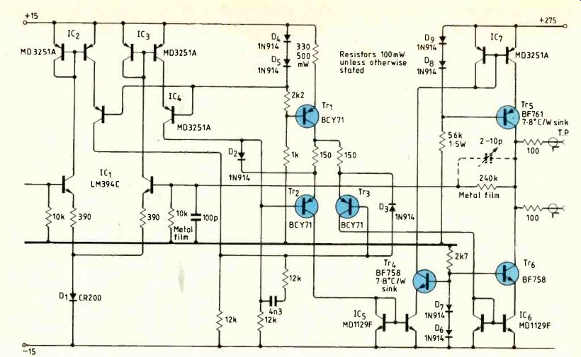
Fig.6. Complete circuit diagram of one version of amplifier.
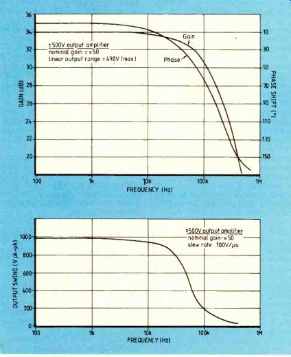
Fig.7. Characteristics of the design arranged to drive a capacitive
load at 20kHz, with a gain of 50 and 1000Vpk-pk swing. This design shown
in the photographs.
Currently the highest rated p-channel power-fet which is available will withstand 500V, so that for outputs of more than 500V the complementary source follower cannot be used. A circuit having similar properties but using only n-channel devices is shown in Fig.5.
Stability and transient response. The design of a feedback amplifier normally commences from a knowledge of the required gain and of the stability of this gain against circuit parameter changes. These two data immediately determine the feedback fraction G3 and the low frequency loop gain Ao, so that the required open loop gain Ao is known. A major advantage of the present method of design is that Ao can be adjusted to the required value, and this has a significant effect upon the problem of achieving a.c. stability and the desired transient response.
To reduce phase shift in this circuit at high frequencies, transistors should be selected whose fT is at least one and prefer ably more orders of magnitude higher than the desired 3 dB frequency of the amplifier.
Transistors in the common-base configuration have a current gain which falls by 3 dB at approximately fT and current mirrors behave in the same way as common-base transistors having transition frequencies of fT/2.
The input stage will have a small input capacitance at each base reduced by the emitter resistors, and one of these capacitances will form a time constant with the feedback potentiometer. This time constant may be compensated in the usual manner in order to make Beta independent of frequency.
Often in order to bring the compensating capacitor to a practical value it will be necessary to add capacitance at the base of the input stage.
Two situations now arise. If the load is current driven, effectively by the output of the intermediate stage, the feedback circuit will form part of the load and the overall time constant will be large compared to 1/wT. If on the other hand the load is driven by a source follower or a totem pole stage, the load time constant will become insignificant compared to that at the input of that stage.
In either case one significant time constant will exist in the output stage. For example in the circuits of Fig. 4 and Fig. 5, the dominant time constant is (Coss-Crss)R. A second significant time constant will usually arise at the input of the intermediate stage.
If the significant time constants are one or two orders of magnitude greater than the remainder, as is often the case, then these latter may be ignored at least to a first approximation, and the amplifier is essentially one with two lagging time constants. If A_Beta 3 >> 1, then for a non-oscillatory step response it is necessary that the ratio of these time constants be at least 4A43. The compensation circuit consisting of C and R at the input to the intermediate stage enables this ratio to be adjusted as shown in the appendix, so that an acceptable transient response may be achieved.
EXAMPLE OF METHOD
As an example of the design method suggested above, an amplifier to meet the following requirements is considered here.
The load is a capacitance of 200 pF in which a non-oscillatory response of 250V is required to an input step of 10V. The output is to reach 99.9% of the final value within 21.r.s, and the gain stability required is 0.1%.
The suggested circuit is shown in Fig.6 and is of the type in which the load is driven by the current from the intermediate stage.
Evidently we need p=1/25 and Ao [3=1000, so that A0=25000. The total current in the intermediate stage must yield a slew rate of at least 125V/0 and thus must be at least 2 x 10^-10 x 250 x 1000/2 x10^-8=25 mA. The total current as designed is 28.5 mA.
The transistors BF758 and BF761 are video devices chosen to withstand 300V, and, with suitable heat sinking, the greatest mean dissipation of 4 W: their fT is 45MHz and minimum hFE is 40. The current mirrors have minimum values of hFE= 100 and fT=200MHz. The BCY71 devices chosen for the intermediate stage have values hFE typical 200 and fT minimum 200MHz, Cµ=5 pF.
Hence for the intermediate stage gm= 1/ 240, S=4.17 ms, gar=gmmFE=20.80, Cn= gm/2arfT=3.32pF, and hence C+G= 1041.1s.
The first significant time constant is hence T1=(5+3.32)x 10^-12/10^4x 10^-6=8x 10^-8s.
For the .LM394C used for accurate balance, low drift and low noise in the input stage, hFE=500, Cµ=15 pF and fT=60 MHz.
Hence gm=1/390, S=2.56 ms, gir=5.13 µs and Grr=6.8 pF.
The input stage will have a differential mode signal only 1/25 of the common mode signal, so that the contributions of g,1 and C,R to the input admittance may be ignored in comparison with that of Cµ. Thus the capacitance loading the feedback potentiometer is 15 pF, requiring about 0.6 pF compensating capacitance. This value is impracticably small, and to make it more reasonable 100pF is added at the feedback base of the input stage, bringing the compensating capacitance to about 4.6 pF.
In this circuit the time constant T2 is that of the load and feedback network: T2= (200+ 115/25) x 10-12/(10-4/25)=51.15x 10-65.
Also Ao=4.17x 10^-3x2.56x 10^-3/(10^-4x 1.04 x 10^-4)=25035, Ao[3=1001, T2/T1=
639.4. The ratio of the time constants is thus too small and correction is needed.
We require CR=51.15x10^-6, T3T4=T1T2 =4.092 x 10^-12 with T3=4004T4, whence C=3.99 nF for which we use the larger preferred value 4.3 nF, leading to R=12 k. The equal time constants in the closed loop are then each 2T4=6.4x 10^-8s.
With this choice of values the rise time to 99.9% of final value is 9.23T=591 ns for small signals. For signals greater than about 10% of maximum the output rise time is determined by the slew rate of 135V/0, giving 1.85µs for 250V output, which is within the specification.
In this example some typical and some minimum parameter values have been used.
Using minimum values of gain parameters will give assurance of adequate open-loop gain and hence of closed-loop gain stability.
In practice, to deal with the question of transient response either a worst case calculation must be performed, or the values of compensation components may be found by trial in a give case, using the mean values as a starting point.
As a further example, Fig.7 shows some characteristics of an amplifier designed to drive a capacitance load of several hundred pF at frequencies up to 20kHz. A gain of 50 was required stable to 0.1% and an output swing of 500V peak was desired. It can be seen that a swing of 450V peak was achieved at 20kHz. The total noise output was 700 µV r.m.s., which could be improved if necessary by attention to the input stage. This amplifier uses an output stage like that shown in Fig.5. Figure 8 is a photograph of this amplifier.
APPENDIX--STEP-RESPONSE CORRECTION
Suppose the amplifier has d.c. gain A,, and two lagging time constants Ti and T2. The differential equation relating output V0 and input V, when the loop is closed with a feedback fraction 3 is then [A0(3+(1+T1D) (1+T2D)]V0=A0V.
The transient response is determined by the complementary function of the equation, whose nature is in turn determined by that of the roots of the auxiliary equation Ao13+ (1+ Tix)(1 +T2 x ) = 0.
For a non-oscillatory solution it is necessary that the roots shall be real and this requires that (T1+T2)2>4(1+A j3)T1T2 or (T1-T2)2>4Ao 13T1T2. Since in practice Ao(3 »1, it follows that one time constant, say T1, must be much greater than the other, whence T1>4 &13T'T2.
Now suppose that the time constant T1 is at the input of the intermediate stage, and is formed by capacitance C1 and resistance R1 in parallel. With the compensating series CR branch connected, the impedance at this point is R1(1+jwCR)/[(1+jwT1)(1+ jwCR)+jwCR1] which takes the place in the gain expression of the impedance R1/(1+jw T1) which obtains in the absence of the CR branch. The additional branch will thus lead to the gain expression Ao(1+jwCR)/[(1 + jw Ti) (1+jwCR)+jwCRi] (1+jwT2).
If we now choose CR=T2, this becomes A,,/[(1+jwTi)(1+jwT2)+jwCRi] which may be written Aá/[(1+jwT3)(1+jwT4)] where T3T4=T1T2 and T3T4=T1T2+CR1. Thus the two time constants T1 and T2 have been replaced by T3 and T4 whose ratio may be adjusted by choice of C whilst keeping CR=T2.
ACKNOWLEDGEMENT
The author would like to acknowledge the contribution of R.R. Thorp, M.A., senior design engineer in the Cambridge University Engineering Department, in the form of constructive criticism, for the design of the second amplifier mentioned and for Figs 7 and 8.
Barron, M.A., graduated from the University of Cambridge, subsequently researching in nuclear physics and electronics for eight years before entering industry. In 1967 he returned to Cambridge as a lecturer in the Department of Engineering.
------------
Also see:
==========
(adapted from: Wireless World , Jan. 1987)