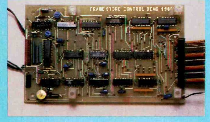
Further details of the control board which, with the memory board described next, is all that is needed to set up a basic system.
by D.E.A. CLARKE
Figure 15 shows the relationship between line sync and the clock. The trailing edge of the sync-derived waveform from Link 2 is differentiated by c103/R106 and the resulting narrow negative-going pulse squared by Schmitt trigger 12.

The resulting pulse, of about 500ns duration, is applied to a n-input of flip-flop Ic103. On the next positive clock transition the output changes state and gates the oscillator, terminating oscillation in the high state. Since there is now no clock to reverse the state of the flip-flop, the trailing edge of the gating pulse is differentiated by c104/ R108 and used to reset IC103 (pin 6) thereby re-enabling the oscillator. After the delay determined by the Lc time constant the clock restarts.
The resulting clock waveform is phase-locked to line with an integral of clock cycles and a short gap when the clock is always high.
DIGITAL SYNC SEPARATOR
In the previous article I described the field sync separator on the analog board. This waveform, designated FS1 in Fig.9, is useful when non-standard video sources are used: but there is an unavoidable tendency to vertical (plus or minus one line) jitter under some circumstances. An alternative sync separator on the control board derives a field sync waveform (Fs2) digitally from the composite (line) sync waveform, and is completely stable. However, this sync separator can normally be used only with standard (CCIR) sync sources. Therefore either field sync waveform can be selected as required by Link 1.
Monostable idol produces a pulse which follows the trailing edge of line sync (Fig.16). For correct operation this pulse must be in the range 4.32 µs: it is also used to provide a horizontal delay for positioning the display window. The pulse is fed to the n-input of flip-flop ic102(2) which is clocked on the negative edge of line sync. In this way the wide pulses during the field sync interval are detected.
ODD/EVEN FIELD DETECTOR
When 512x512 (interlaced) mode is selected it is necessary to identify the order of fields, since the stored frame consists of two. Figure 16 shows that the line sync waveform toggles flip-flop ic102 which is reset during the field sync interval. The output at pin 9 is applied to the n-input of flip-flop íc114(2). The trailing edge of FS2 then clocks ic114(3). The duration of FS2 is critical: it must be 148 ± 16 p.s in order to detect the odd number of lines between successive fields. These lines are identified by the output ic102(9). Duration of FS2 is set by potentiometer P102 and the field identity waveform is available at ic1 14(pin5).
TABLE 1
Link options: all are two way shorting links.
[1] 64K ram. Clock frequency = 5.8MHz approx.
c106=220pF (21256K ram. Clock frequency = 9MHz approx.
c106=0. Connect IC111(10) to íc115(3,4,5.6), not Vcc.
[3] 256K ram. Clock frequency = 11.6MHz approx.
0106=0 Link 1=2
... for non-CCIR interlaced-sync video sources Link 3=1 for increased address hold-time after write (choose to suit ram-chip specification)...
DUAL IMAGE MODE
It is possible to update and display odd and even fields individually in 512 x 512 (inter laced) mode. This is useful for dual-image capture or for 3D display techniques and is achieved most economically by modifying the length of the FS2 monostable pulse by ±32µs (tolerance re mains ±160). The odd/even waveform then remains in a de fined logic state to select permanently one or other of the images. The resulting three modes (odd field select, even field select and interlace select) are determined by switch s2.
Odd/even field identification is available only in 512x512 interlaced mode. For non-interlaced 512x512 mode, ic114(5) is configured as the high order bit of a modulo-512 address counter by links 7,8 and 9 in position 1.
In 256x256 mode, field-detect circuitry is redundant unless required by the host computer for synchronization. Field-sync or field-ident is then avail able to the host via Link 10.
ADDRESS COUNTERS
The major job of the control board is to supply addresses and control signals to the memory. Two counters are employed for this purpose, one to count clock pulses along the line (the horizontal counter), the other to count lines down the screen (the line counter).
Line sync is always the initiator of a horizontal counting cycle (Fig.17), but it is desirable to be able to position the display window horizontally according to the display format and aspect ratio required. To achieve this, monostable ic101(13) delays the start of the counting cycle by an amount determined by potentiometer plop. This start pulse triggers the toggle ic104(3) via the nor gate ic110, the toggle having been reset previously by the last line sync pulse at ic104(1). Clock counters Ic104,105,106 are held in the clear position by 1c104 until this point and are now enabled. For minimum propagation delay ic104 is a 74F74 and it divides the clock by two prior to the address counter ic105/ic106. This is because the memory is configured as 16 bits and two samples are stored per location; more detail will be given later.
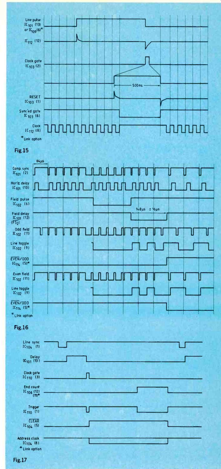
Fig.15 (right): waveforms in the phase-locked clock generator on the
control board.
Fig.16 (middle right): digital field sync timing and odd/even field detection.
Fig.17 (bottom): timing for the horizontal counter.
Link 3 and íc109 provide a selectable delay element concerned with memory write timing. For ic105.106, 74F series devices are used: these are superior to the LS series in that each output is individually buffered and can drive the capacitive load presented by the memory without malfunction. Propagation delay is also considerably reduced, allowing higher sampling rates with slower memories.
Once a count of 128 or 256 (depending on Link 4) is reached, ic104(3) is triggered again and the horizontal display cycle terminated until re-started by the next line-sync pulse.
The counters are inhibited during the field.
The line counter works in an almost identical fashion to the horizontal counter except that the mechanism for positioning the display window vertically is necessarily different (Fig.18).
Line syncs are applied via Ic110 to the binary counter ic115 which is held in the cleared state by field sync. When field sync ends, the counter increments until the inputs of the gate ící11(9,10) are both high (after three lines or 35 lines depending on Link 5), at which time the counter input is inhibited by Ic110 pin 6. The inhibit output ic111(8) then starts the line counter ic1I6 via ic114(8) in a similar manner to the horizontal counter. The terminal count is either 256 or 512 depending on Link 6 and the configuration of IC114.
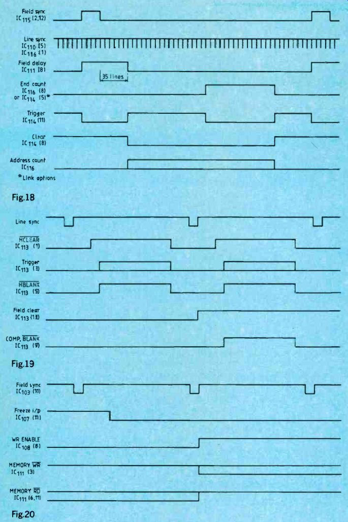
Fig.18 (left): timing for the line counter on the control board.
Fig.19 (middle left): generation of blanking waveforms.
Fig.20 (below, left): memory read-write mode timing.
BLANKING GENERATOR
Blanking is derived from the address counter clear waveforms (Fig.19). The start of horizontal blanking is initiated by the first positive address transition at ic105(12) clocking a logic 1 through flip-flop ic113(3). This delay is necessary because the first few memory locations contain invalid data.
Horizontal blanking generator Ic113(1) is reset at the end of the horizontal counting cycle. The horizontal blanking output ic113(5) is then retimed by Ic113(12) and held in the cleared state by the vertical display window waveform at ic113(13). Composite blanking appears at ic113(9) and is combined with the c.p.u. blanking signal in ic112(3) before being sent to the analog board.
MEMORY CONTROL
The frame store has two operational modes: memory write (continuous display update) and memory read (display freeze).
Switching from one to the other must occur on a field sync transition (Fig.20). This is ensured by D-type flip-flop ic1o3(8,9) which retimes the freeze command from the c.p.u. (if connected) or the freeze switch. When this signal is low the memory is continually updated and live video is seen on the screen: when high, memory is read continually and stored video is seen on the screen.
Memory control waveforms are derived from the clock divider ic104 in conjunction with gates ic111 (3,6,11), and will be discussed in detail in the next article. Wave form LE at ic112 (6) is used to tri-state the a.d.c. latch on the analog board whenever data is read from the memory or c.p.u.
COMPUTER INTERFACE
The computer interface is the simplest possible, consisting of six control inputs applied via the buffer Ic107. Pull-up resistors ensure the correct operating state when the c.p.u. is disconnected, while limiting resistors pre vent latch up. The use of a 74HCT series device results in simpler driving requirements because of its low input current.
The c.p.u. control input Ic107 pin 13 blanks the screen and selects c.p.u. access via the data selector Ic108. Complete control of the store is then gained by emulating the clock, line-sync, field-sync and mode inputs to increment and reset the address counters and select update or freeze mode.
Computer interfacing techniques will be discussed in a later article.
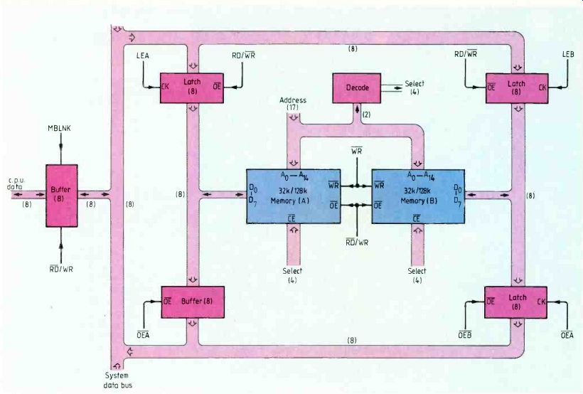
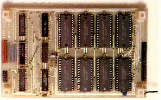
Fig. 21.Outline of the memory board. A choice of ram chips may be used,
for single-field or full-frame storage.
MEMORY BOARD
Next we turn our attention to the memory board and power supply. These two items are all that are now required to get the basic frame store up and running.
Display resolution of the basic unit is 256x256 with 256 grey levels. This translates to a memory requirement of 64K bytes.
Until recently, dynamic ram chips would have been the only option for this amount of storage because the cost of static ram would have been prohibitive: but 64K static rams are now relatively cheap, and although more expensive, bit-for-bit, than dynamic, their advantages outweigh their extra cost.
The advantages of static ram in this application are:
--lower total power consumption because refresh is not required.
--reduced cycle time (equal to access time) compared with dynamic equivalents.
--minimal control circuitry and greatly simplified computer interfacing through the elimination of refresh.
Their increased board area occupancy is more than offset by reduced circuit complexity and chip count.
MEMORY ORGANIZATION
The 256x256 display format results in a pixel rate of 5.8MHz, assuming 44 uS active horizontal display period and 11.6MHz for the 512 x 512 option. The latter is equivalent to an 86 ns memory cycle. Using sub-86ns rams would be very expensive and wasteful, since by storing two samples/pixels per memory location (by organizing the memory as 16 bits per address location), the memory cycle-time can be doubled to 172 ns and cheap 150 ns rams used. A minor penalty is the requirement for latches to hold data temporarily as it is written to and read from the memory. The overall arrangement is shown in the block diagram. Fig.21.
The ram is split into two blocks, A and B, but only the data i/o pins are separate: all other inputs, address, RDIWR and chip enable are commoned, so that data is read and written simultaneously as a 16-bit quantity Latches are shown for holding input data during write-mode and a latch-buffer for holding-steering output data in read-mode. There are four 16-bit memory banks (eight ram chips in total). The two high-order address bits from the line counter are decoded to select the appropriate bank.
To enable an external computer to access the memory, a bi-directional buffer is also on this board.
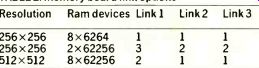
TABLE 2: memory board link options
MEMORY CIRCUITRY
The memory circuit is shown in Fig.22.
Links are provided to configure the board for eight 64K or two 256K devices (256x256 display) or eight 256K devices (512 x 512 display).
Address decoding (Ic208) takes place on line boundaries, when access time is least critical. Access to the c.p.u. is via ic207 which is a 74HCT245 with pull-up resistors. The series resistors are to prevent latch-up and should be shorted when driving non-mos ports etc. on the host computer. Output data from block A does not require latching and an 8-bit buffer Ic201 suffices.
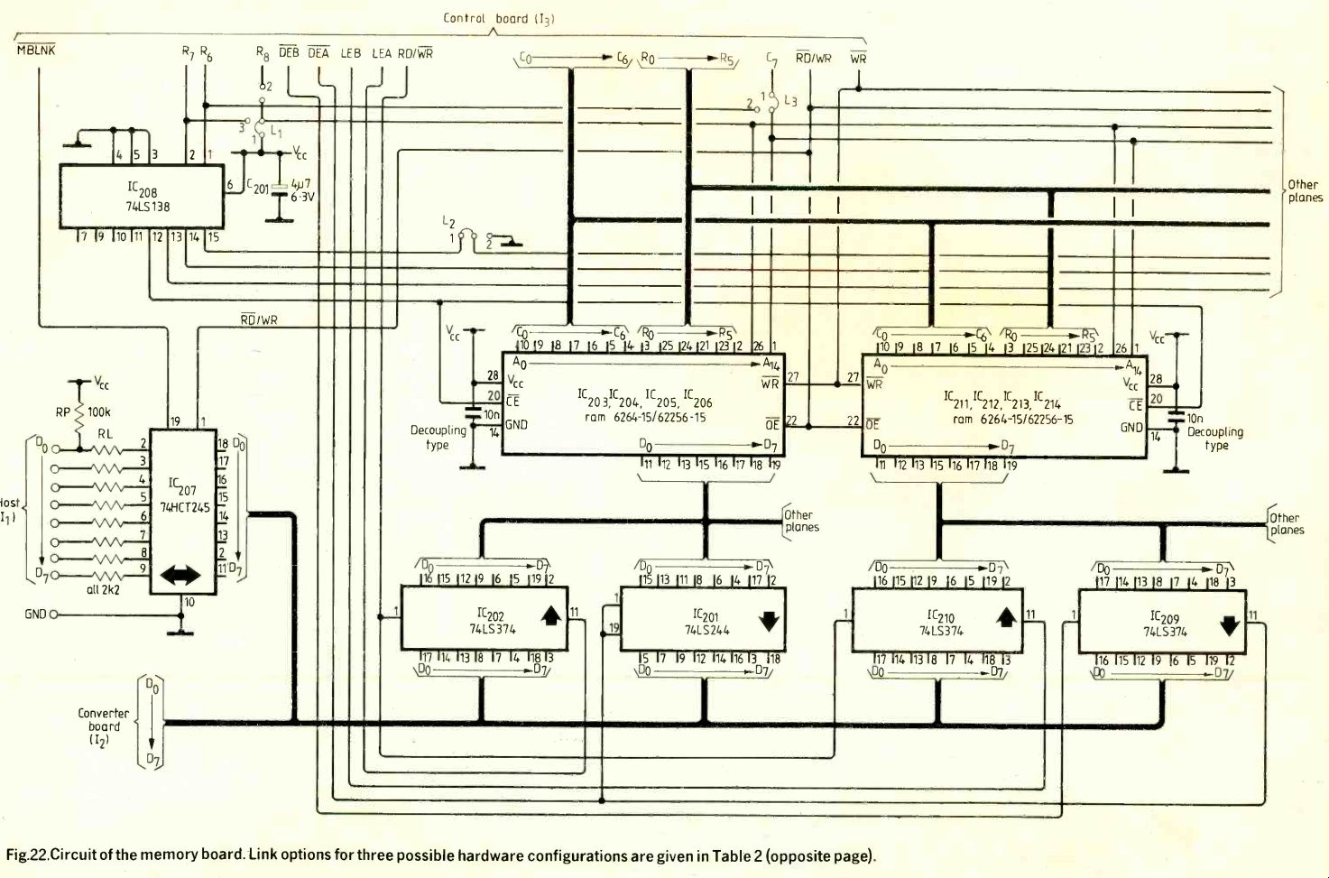
Fig. 22. Circuit of the memory board. Link options for three possible
hardware configurations are given in Table 2 (opposite page).
MEMORY OPERATION
The memory operates in two distinct modes (controlled by the freeze signal), read-mode and write-mode, RD/WR determines which mode is active. During memory write, live digitized video is displayed on the screen.
To be continued ...
------------
Also see:
==========
(adapted from: Wireless World , Jan. 1987)