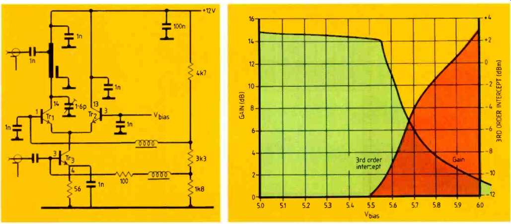
900MHz gain-controlled amplifier
Transistors in this 900MHz amplifier with voltage-controlled gain are all from one i.c. Plessey's SL2364/5 arrays consist of two long-tail pairs whose tail transistors are internally current-mirrored to similar transistors. Typical ft of the bipolar devices is 5GHz.
Collector load in the amplifier is a 14mm length of 7551 stripline resonated with a 1-6pF capacitor. A small loop of stiff wire grounded at one end and located a few millimeters above the stripline forms the transformer secondary winding. Graphs for gain and third-order intercept versus voltage bias are shown. At full gain, noise is 9dB.
Other circuits in the SL2364/5 application note are a 150-300MHz frequency doubler, a 100-300MHz frequency tripler and a single-balanced mixer. These circuits have neither coil winding details nor explanatory text.
-----------------
Mixer design using admittance parameters
Using small-signal admittance parameters simplifies transistor mixer design. Note AN238 from Motorola details the technique and presents three design examples including this mixer for converting 30MHz r.f. to 5MHz i.f. using a 35MHz local oscillator.
Both local oscillator and r.f. signals are base injected. For the 2N2221A working at 2mA collector current and 10V collector-emitter voltage,
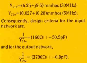
Full equations for obtaining component values are included in the note. Characteristics of two further mixer circuits, both for 250MHz conversion to 50MHz output, are also given.
----------------------
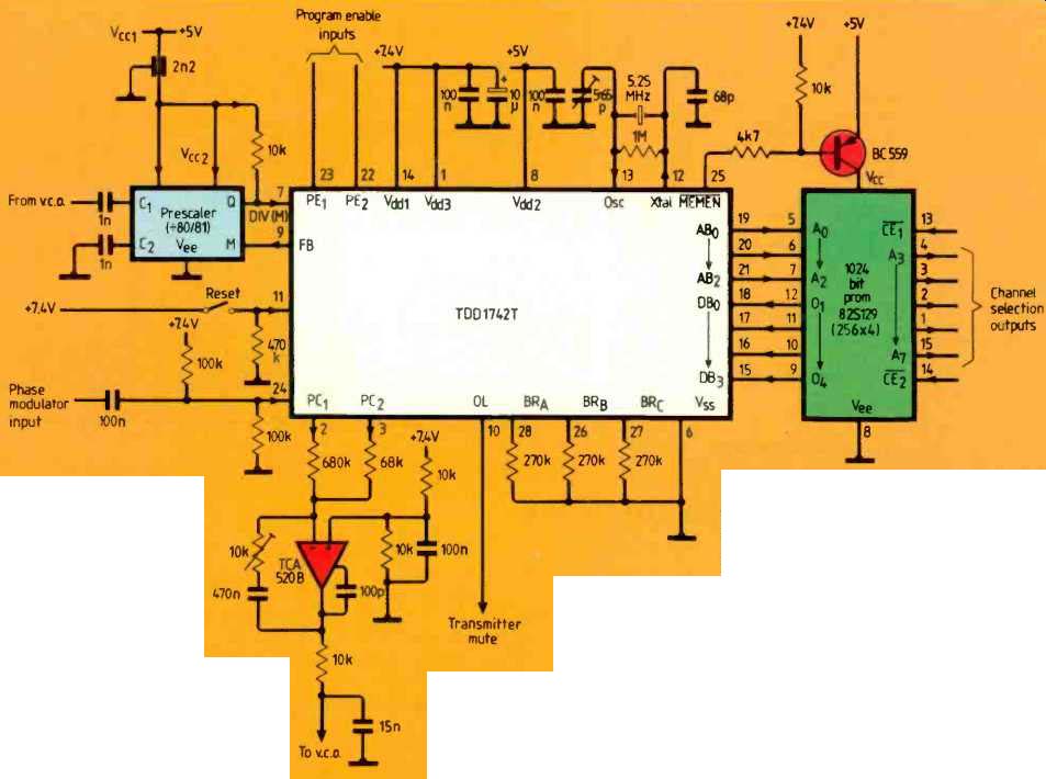
Low-power frequency synthesizer
Features from both the 4750 frequency synthesizer and 4751 universal divider are included in one bus-programmable frequency synthesizer designated TDD1742. Designed for low-power v.h.f./u.h.f. synthesis, 1742 is suitable for portable and mobile radio applications. It has a high-gain phase comparator with sample-and-hold capacitor and phase-modulation circuits.
Frequency range of this application circuit from Mullard's TDD1742 development data sheet is 150-155MHz. Input frequency is reduced to less than the device's 8.5MHz limit by an external prescaler. Fixed and programmable dividers reduce 5.25MHz crystal frequency to a 12.5kHz reference which feeds the device's two phase comparators. Sensitivity of the v.c.o. is 1MHzN and loop bandwidth is 300Hz.
At power up, pin 25 being high determines that the device will operate in memory mode, i.e. programming data is read from rom. For operation directly from a micro-controller, pin 25 is held high and programming data is strobed into the device externally. With the phase modulator off, supply current is less than 1.5mA; minimum supply voltage is 7V.
---------------
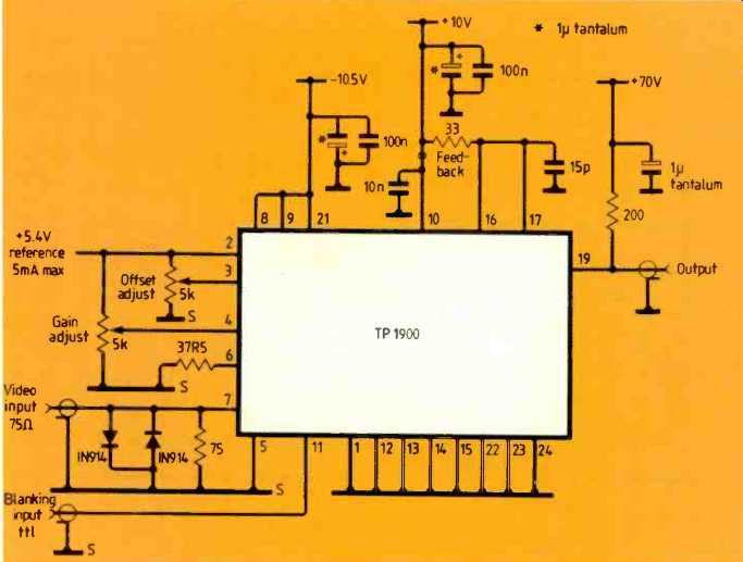
175MHz video amplifier/driver
A differential preamplifier, variable-gain stage and class-A output stage within the TP1900 convert 75 ohm video input at 714mV (RS170) to c.r.t. cathode drive. For a 55V swing into 200 ohm and 6pF, output rise time is 2.5ns so the device is suitable for high resolution monitors; gain is variable from 0-85V/V.
Here the device is shown connected for 0.5V common-mode input, and output from a 5.4V buffered zener reference feeds gain and offset potentiometers. Blanking input sets output to 2V below the black-level, which is set using the offset control. This circuit is from the preliminary data sheet for he Teledyne TP1900.
==========
(adapted from: Wireless World , Oct. 1987)