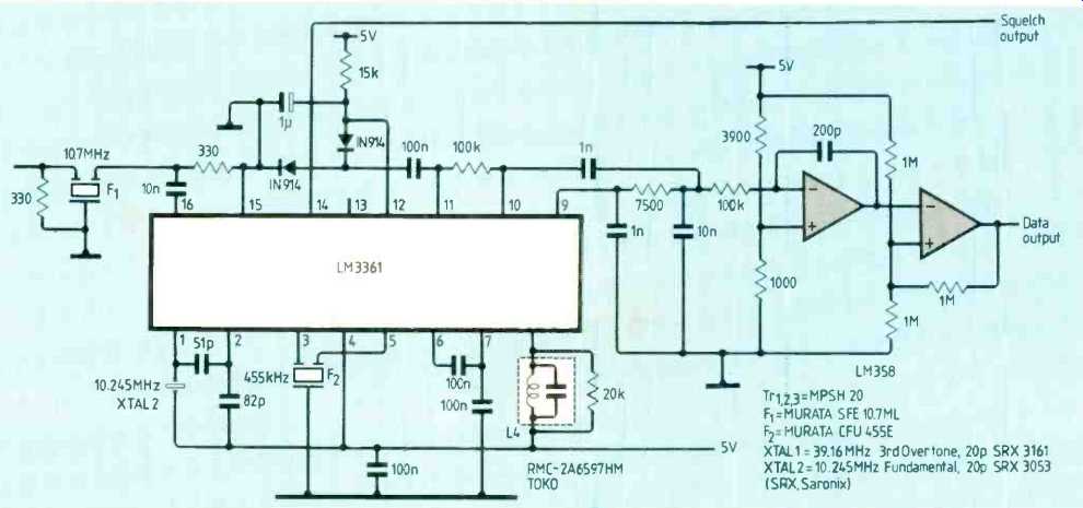
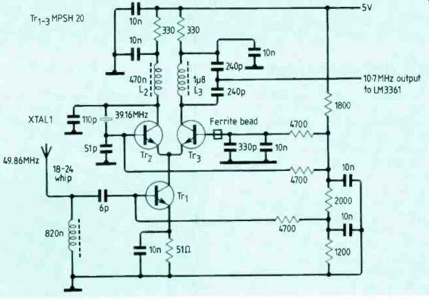
FSK data receiver
Digital communications and telemetry are popular uses of the American 49.82 to 49.9MHz band* for low-power devices operating up to about 30m. A simple yet effective f.s.k. receiver for this band can be made from an LM3361 narrow-band FM i.f. amplifier/detector.
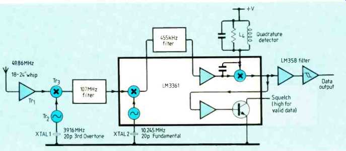
Incoming carrier centered at 49.86MHz is converted to two intermediate frequencies of 10.7MHz and 455kHz. Both i.f’s include readily available ceramic filters to increase selectivity while reducing coil count. Base band data is recovered using quadrature detection and an integrator/Schmitt-trigger filter demodulates output. The squelch circuit also functions as a status indicator; when signal is present, its open-collector output switches high.
Consumption of the 3361 is 4mA at 5V--the entire circuit consumes about 10mA.
With components shown, typical detector conversion gain is 150mV for each kilohertz of carrier shift. Frequency shift of 3.3kHz results in 500mV pk-pk detected output at pin 9. Increasing the Q-setting resistor at pin eight gives higher gain.
Many transmitters have a 16.62MHz master oscillator tripled to 49.85MHz. Modulation is carried out by pulling the 16.62MHz fundamental crystal: pulling of more than 1 kHz is possible, which gives 3kHz when tripled. By comparison, a 49.86MHz third overtone crystal could only be pulled by a few hundred hertz because crystal Q increases as the square of the harmonic order.
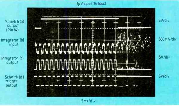
Significant baseband filtering is illustrated in the first (lower) oscillogram.
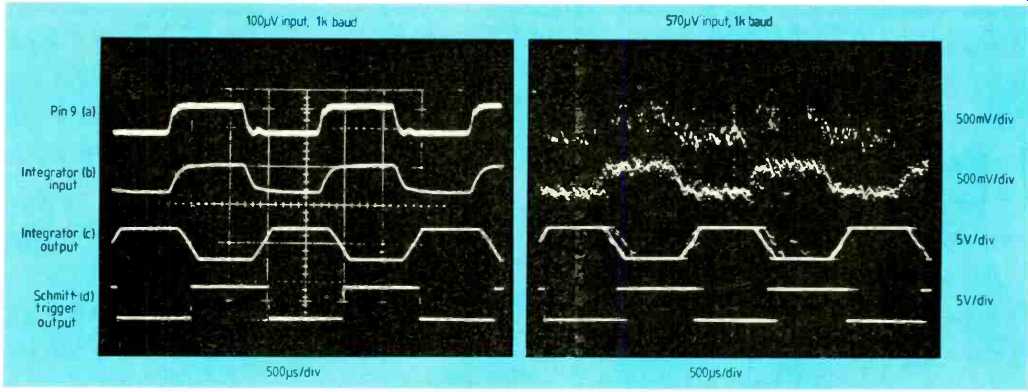
Twice-i.f. product of the quadrature detector, evident in the top trace. is removed by RC filtering at pin nine. Weak-signal performance is shown in the second oscillogram. Input of slightly less than 570nV results in about 10% jitter at 1 k-baud. At 500nV, the occasional bit is lost and at 300nV the squelch line goes low. although data is still visible at the output. On and off times of the squelch switch are 3 and 1ms respectively. Despite the squelch on time, data at pin nine appears almost immediately. as shown in the top oscillogram. Correction of the d.c. output shift occurs within 1 or 2ms.
Bandwidth limitations of the 455kHz filter, integrator, transmitted signal and L4 limit the data rate to 1.2kbaud. Long strings of ones and zeros are not a problem since the circuit is d.c. coupled. When testing the circuit note that r.f. generators with FM input, like the Boonton 103/1020. cannot produce f.s.k. because their FM input is a.c. coupled.
A relatively short whip antenna of 460 to 610mm, is matched to r.f. amplifier Tr1 by an 'L' network of 4-6pF and 50-100 ohm in series. It is a common misconception that a short 49MHz whip exhibits just a few ohms.
While this may be true, impedance measured from the base of the whip to ground is 50 to mon in series with a capacitive reactance of about 4-6pF. High driving--point resistance is a result of a lossy ground, not the whip.
To tune the circuit, connect a carrier of <2p.V modulated by alternating ones and zeros and adjust the quadrature coil while observing integrator output. Tune L4 for symmetrical trapezoidal waveform at the integrator output. With crystal tolerances of 0.005%, no other adjustments are necessary. Receiver sensitivity can be peaked by adjusting L1.
Mitchell Lee; National Semiconductor; Santa Clara
-------------------
Frequency control in Wien-bridge oscillators
Adding an op-amp inverter to the conventional Wien bridge oscillator provides frequency control.
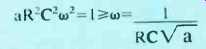
For a normal Wien bridge oscillator, the condition for oscillation is R iCiR2C2= I. By adding an inverter it is possible to change current through one of the bridge resistors.
If inverter gain is 1/a then the left part of the expression, the condition for oscillation, is multiplied by factor a.
In this oscillator, R1=R2=R, C1=C2=C and the condition for oscillation is
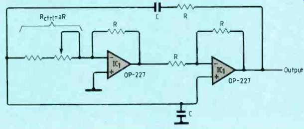
Frantisek Michele; Brno, Czechoslovakia
==========
(adapted from: Wireless World , Oct. 1987)