By CHARLES YAGER and HARLAN OHARA
This highly-integrated device offers better performance than board-level systems and cuts the workload of the controlling CPU to manageable proportions.
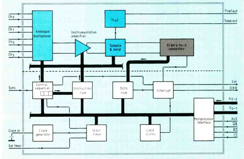
Fig. 1. The ML2200 data acquisition peripheral is a complete data acquisition
subsystem on a single low power chip. It offers high performance at a lower
overall than for board-level systems cost.
Until now, designing a data acquisition subsystem has called for a design engineer experienced in both analog and digital circuitry. Usually the task begins with the selection of the a-to-d converter; however, with 12 to 13 bit a-to-d converters, little system support is provided other than the converter itself. A myriad of both analog and digital components still needs to be added to complete the interface.
Designing the analog section of a data acquisition system requires several ICs and in many cases a number of precision discrete components. A typical analog section consists of an input multiplexer, a sample-and-
hold amplifier, a programmable-gain instrumentation amplifier and a voltage reference, in addition to the converter. While several 12 to 13 bit a-to-d converters offer some combinations of the above capabilities. none offers them all. This leaves the designer with the formidable task of matching the right analog components with the converter and the thorny task of achieving a low noise layout.
Once the analog components of the system have been matched, stability must be considered. Generally, the current crop of converters requires external trimming for both bipolar offset and full-scale error. While external trimming does improve the offset, recalibration is needed periodically during the life of the system. Schemes have been devised for self-calibrating bipolar offset and full-scale error, but they come at the cost of special calibration software and additional board space for the extra circuitry. Even the addition of gain and offset auto-calibration circuitry cannot improve linearity specifications, which are inherent in the converter and subject to temperature and time variations.
Currently, 12 to 13 bit a-to-d converters provide little digital capability other than a double-buffered generic microprocessor interface. With this low level of digital capability at high sampling rates, a considerable load is placed on the microprocessor, exhausting it with the i/o task and effectively rendering it useless for application processing. Additional digital logic can be designed into the subsystem to offload the micro processor: however, again, this requires extra circuitry.
---------
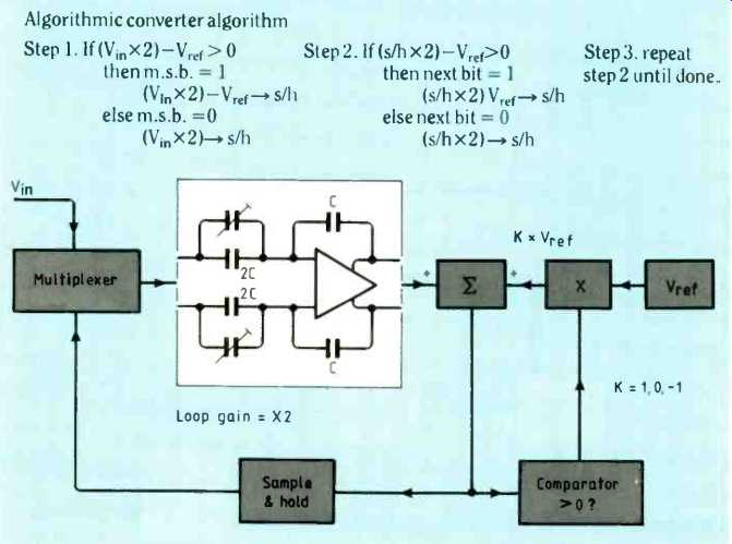
Self-calibrating algorithmic a-to-d converter
Algorithmic a-to-d conversion is one of many successive approximation techniques. One popular technique uses a DAC to feed back the approximated signal. The difference between the approximated signal and the original signal is used to convert the next bit This solution requires more circuitry since each bit in the DAC requires two resistors, and the resistor values need to be matched to within the accuracy of the number of bits of the a-to-d converter.
The algorithmic converter only uses a 2 , amplifier (using input and feedback capacitors to realize the gain of 2) and a sample-and-hold amplifier. The algorithm employed is basically binary division where the input voltage is divided by the reference voltage (V,./V-1).
Conversion begins by multiplying the input signal by two. The reference is then subtracted from this signal and the difference is compared to 0V. If it is greater, the MSB is 1 and the difference is stored in the sample-and-hold circuit If the difference is less than 0V, the MSB is 0 and the reference voltage is added back to the difference and stored in the sample-and-hold circuit During the second and subsequent times around the loop. the sample-and-hold voltage is multiplied by two and the reference is subtracted from it. The algorithm is a slightly modified for negative input voltages.
----------
TWO-IN-ONE CHIP
These design problems have found a solution in a single, integrated component that uses a systems-oriented approach to data acquisition. Micro Linear's ML2200 data acquisition peripheral (d.a.p.) offers an entire 13-bit data acquisition subsystem on a single c-mos chip which provides higher throughput and better analog specifications than conventional designs (Fig. 1).
At the heart of the d.a.p. is a 13 bit self-calibrating a-to-d converter (12 bit plus sign). Complete conversions, including the sample and hold, run at 40kHz for 13 bits, and 50kHz for eight bits. The ML2200 requires no external components--including trimming devices--which can drift over temperature and time.
The four-channel differential input multiplexer feeds the input signal into a high-precision, programmable gain, instrumentation amplifier. Each channel can have a different gain selection, which is automatically controlled by the on-chip processor.
Completing the analog section is a sample-and-hold amplifier and an on-chip voltage reference. The sample-and-hold amplifier allows programmable acquisition time for high-impedance input signals. However, with only a 2 uS acquisition time--the default--output impedances of up to 10k-ohm can be accommodated while still maintaining 13 bit accuracy.
Following transfer of the input sample, this same amplifier samples the reference source selected in software. Since both the reference and the signal pass through the same sample-and-hold, there is no gain error between the source and reference: thus full-scale accuracy is guaranteed by design.
The internal voltage reference is a 2.5 volt bandgap reference with an accuracy at room temperature of ±5mV and a maximum temperature coefficient of 50 p.p.m. per degree Celsius. When performing a conversion, the ML2200 provides the option of using the internal source or one of the four external channels as a voltage reference.
This allows ratiometric conversion between any two of the four channels. Ratiometric measurements can also be taken without sacrificing an input channel using the Vref output pin. For example, Vref could be used as the supply voltage for a resistive bridge type of sensor, such as an i.c. pressure transducer.
The Vref circuit also produces a TEMP OUT signal, a voltage proportional to the die temperature. Because of the low chip power dissipation, the die temperature is only 10-15°C above ambient. Therefore TEMP OUT could be fed into one of the input channels, informing the microprocessor of the system temperature. If excessive temperature conditions are important to know, the ML2200 could detect this condition via the on-chip level alarm and generate an interrupt for the microprocessor.
A-to-D CONVERTER
Choosing an algorithmic converter for the 13 bit a-to-d was a critical part of the ML2200's design. There are several advantages to using an algorithmic converter (see box):
--it uses relatively little die area, therefore allowing room for other functions
--it is easily made fully differential, removing the effects of power supply coupling
--linearity of the converter depends on only two parameters: the gain error in the loop and the offset error in the loop. The offset error is eliminated by the auto-zeroing circuits in the sample-and-hold and 2x operational amplifiers: this is done at the beginning of each conversion. The 2 x gain of the loop is precisely controlled by the self calibration circuitry.
Once the offsets have been nulled, the algorithmic converter is calibrated by measuring the 2 x gain of the loop and adjusting it. Cain can be measured by converting the internal voltage reference.
The result, in the ideal case, is all Is. If the loop gain is slightly less than 2. the resulting l.s.b. of the conversion will be 0. If the resulting conversion is all Is, the gain may be too great and is reduced until the threshold of the l.s.b. is reached.
Adjusting the gain of the loop is done by tuning the binary-weighted trim capacitor array for each of the 2C input capacitors.
This must be used differentially so that it can either increase or decrease the 2C value by being connected as positive or negative feedback.
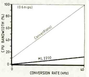
Fig. 2. A conventionally double-buffered a-to-d converter requires an order
of magnitude more CPU bandwidth then the ML2200. For a standard 0.6 mips micro-controller
at a conversion rate of 40kHz, the entire bandwidth is consumed by the overhead
of interrupt processing.
Calibrating the a-to-d converter is a simple matter of programming. Once the ML2200 has been powered up, the CPU sets the cm. bit in the control register and the device goes into its self-calibration mode.
Since calibration takes 2ms to perform, the ML2200 generates an interrupt when it is complete, allowing the CPU to execute other tasks while calibration is executing.
Self-calibration should always be executed on power-up before the chip is placed in the run mode. Re-executing self-calibration can be done at any time.
ON-CHIP DIAGNOSTICS
The d.a.p.'s built-in diagnostics provide a way for the system to ensure that the chip is fully operational and meeting specification.
To test the digital paths within the chip a digital loopback is provided, guaranteeing that the internal data paths and registers are fully functional. The analog section provides several diagnostic features testing linearity, bipolar offset, full-scale error and common mode rejection ratio. To ensure that the self-calibration circuitry is functional, the user can read the calibration code result. This code informs the system that the calibration circuitry was able to adjust the linearity to within ± ½ l.s.b. at 13 bits.
Converting with the inputs shorted to ground provides system offset values, ensuring bipolar offset is within specification. Converting the internal voltage reference provides the full scale error. Converting with both inputs shorted to Vrd provides a common mode test. No external circuitry is required to support diagnostics.
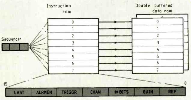
Fig 3. Each instruction from the instruction ram causes an a-to-d conversion.
Up to eight conversions can be stored on chip before a request to read the
buffer is issued. The double buffered architecture allows up to eight more
conversions while the previous series of conversions is being read.
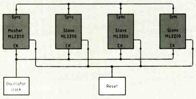
Fig. 4. Several ML2200s are easily synchronized by tying the sync pins together
and running them off of the same clock. The CPU can internally program the
sync pin to be an output (master) or an input (slave). One application of this
technique is to achieve higher order sampling. The master d.a.p. issues a sync
pulse which triggers the slaves to sample the same signal. Each slave uses
the internal 16 bit timer to delay the appropriate amount before sampling the
input signal.
DIGITAL SECTION
The digital section of the ML2200 was designed with three basic goals in mind: to offload the microprocessor, provide a high performance standard peripheral interface requiring no external support circuitry, and offer a highly-programmable solution for maximum flexibility.
To accomplish these goals a programmable processor is integrated into the nucleus of the chip. autonomously controlling the entire operation of the d.a.p. The on-chip processor contains eight instruction ram locations, or operations. Upon system power-up, the microprocessor loads the ML2200's instruction ram with a particular system configuration. The microprocessor can dynamically change the instruction ram to adapt the ML2200 to changing environments or system configurations.
Once the d.a.p. has been initialized, it can run autonomously without CPU intervention. As conversions are completed, data is buffered in the on-chip data ram. Up to eight conversions can be buffered before the chip notifies the CPU, through an interrupt or d.m.a. request, that the buffer is full. The double-buffered architecture allows eight more conversions to be taken while the previous series of conversions is being read.
On-chip limit alarms provide even more opportunity to off-load the CPU These can generate interrupts based on two programmable voltage levels as well as in-range and out-of-range detection. Interrupts can also be generated if the a-to-d converter goes into over-range or under-range. Having the ML2200 automatically scan for a-to-d saturation or programmable voltage levels frees the microprocessor from having to scan each converted data word for these conditions.
Programmable timing control is achieved using the on-chip 16 bit timer: this can be used for a variety of data acquisition functions. In one of its modes it acts as a programmable sampling clock, generating precise sampling rates independent of microprocessor control. Programmable sample-and-hold acquisition times are another feature of the 16 bit timer--this feature is handy when input channels coming from a high-impedance source require longer acquisition times.
The 16 bit timer can receive its clocking source from either the internal clock, running at 4MHz, or an external input pin (TCLK). Therefore, if the internal clock cannot provide an exact enough frequency, or if the timer must be synchronized from an external source, the TCLK pin is available. This pin can also be used as an event counter, counting n events before triggering a con version.
CPU OFFLOADING
The combination of autonomous operation, eight word double buffering, level alarms, and the 16 bit timer dramatically reduces CPU loading, freeing the microprocessor for other tasks.
As an example, consider a design using a single-chip microprocessor for the CPU of a data acquisition system. Typical performance of a standard single chip micro processor is about 0.6 million instructions per second (mips). Conventional a-to-d converters provide only double buffering: there fore an interrupt would be generated for each sample. Since the ML2200 contains an eight-word double-buffered data ram, the interrupt frequency is reduced by a factor of eight.
A typical interrupt service routine would take 9-15 instructions, not including the time taken to read the data and store it, which is equal in both cases. Assuming an alarm feature is incorporated, another 3-5 instructions would be required with a conventional a-to-d. The ML2200 handles this automatically. Thus. using a 40kHz sampling rate, a conventional converter would take between 0.48 and 0.8 mips (40kHz x9-15 instructions). which is 80% of the CPU's bandwidth. The ML2200 requires 0.045-0.075 mips (Fig.2).
Considering the amount of CPU band width consumed by i/o for a conventional a-to-d converter, it is plain to see that no capacity remains for application processing.
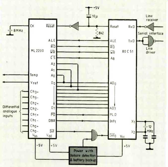
Fig. 5. A direct interface to standard microcontroller provides a highly-integrated
solution for a remote data acquisition system. Since both chips are in cmos.
this application consumes very little power and can even accommodate a power-down
mode.
CPU INTERFACE
As the frequency of peripheral interrupts increases, so does the value of a high performance bus interface. Adding wait states to i/o cycles wastes CPU time and slows overall throughput. Micro Linear's d.a.p. provides an 8MHz no-wait-state inter face, which maintains system performance and eliminates the need for wait state glue logic.
Other ways to enhance system performance via the microprocessor interface include a variety of high-performance i/o methods. The three standard types of i/o, from the lowest to highest performers, are polling, interrupts and d.m.a. The ML2200 offers all three.
Polling is by far the most inefficient i/o method, consuming the most CPU band width: however it also requires the least amount of logic. Interrupts provide the next level of performance, because the CPU is relieved of polling on-chip registers, but the CPU still needs to do a fair amount of processing for each interrupt request.
One of the tasks involved in interrupt processing is determining the source of each interrupt request. Since the d.a.p. contains seven internal interrupt requests, the CPU would have to read the interrupt status register and execute a routine to resolve which interrupt was being requested.
However, the routine would have to be executed every time an interrupt occurs. By far the highest frequency of interrupt re quests comes from the data.
For this reason, the d.a.p. has two interrupt request i/o pins: one for data (data buffer ready--on) and another for the less frequent interrupt requests (INT). If the system cannot afford two separate interrupts, the data buffer ready request can be mapped into the INT pin.
Direct memory access provides the highest performance i/o. When the ML2200 is placed in d.m.a. mode, the DBR pin serves as the d.m.a. request while the INT pin serves as the interrupt request. The DIM pin is activated when the data ram is full and remains active until the data buffer is empty, thus allowing burst-mode d.m.a. (back-to-back cycles).
The peripheral interface on the ML2200 is no different from any other microprocessor peripheral such as a u.a.r.t. or a floppy disc controller. The only external component required is a crystal, which can be substituted for a TTL-compatible clock input.
Saving external logic is the main reason for including an address latch enable (ALE pin.) The ML2200 has the ability to operate on multiplexed or non-multiplexed buses with no additional glue logic. When the d.a.p. is used with multiplexed buses, ALE removes the need for an external latch.
Address information is latched on the address pins on the falling edge of ALE. For non-multiplexed buses, ALE is simply tied high.
Another cost-reducing feature of the ML2200 is its power consumption, which is about a quarter of a watt, or less than one eighth of the power of equivalent discrete solutions. In addition, the chip can be placed in a power-down mode, by pulling the pl) pin low, which consumes less than 1mW. All register contents are retained. even without a clock input. Restoring the power fully restores and operation of the chip without the need to reinitialize it.
PROGRAMMABLE PROCESSOR
In the d.a.p.'s programmable processor is a sequencer that sequentially executes instructions from the on-chip instruction ram. There are eight programmable instruction ram locations where each is an operation (Fig. 3). On initialization the micro processor loads the instruction ram with the desired operations by writing to the on-chip instruction ram registers.
After the ML2200 has been initialized, it is placed in run mode where the sequencer cycles through the instruction ram. decoding and executing the operations. Each operation stores converted data in the corresponding data ram location.
The eight instruction ram locations are 16 bits wide and are broken up into seven different fields:
LAST: indicates that this is the last operation.
ALRMEN: arm the limit alarm for this operation.
TRIGGR: start conversion criteria-immediate execute (full speed mode)
pause and wait for microprocessor to initiate start
start on next timer timeout
preset timer and wait for timeout
wait for external sync signal
preset timer by sync signal and wait for timeout CHAN: channel to be converted.
BITS: number of bits to convert-8 bits (7 bits plus sign) or 13 bits (12 bits plus sign).
GAIN: gain select: 1, 2, 4, 8.
REF: reference to be used--internal V, (2.5V) or external channels 0 to 3.
The rate at which the sequencer cycles through the instruction ram is a multiple of the channel sampling rate. If a channel is sampled only once per cycle, then the cycle frequency is also the sampling frequency. However, the same channel can be sampled more than once per cycle, which is important when channels have different band width requirements.
When the sequencer is free-running at its maximum speed (immediate execute), several signals can gate or inhibit the sequencer from executing the next operation, which effectively lowers the sampling rate even though the conversion time remains the same.
One of these is the external sync pin. This feature allows the d.a.p. to synchronize conversions to an external event. The pin can be programmed to be an output or input.
When SYNC is an output, the ML2200 becomes the master and a positive going pulse is activated just before the beginning of each operation. As a slave, the ML2200 waits for the SYNC input before executing the next operation.
MULTI-CHIP SYNCHRONIZATION
Several ML2200s can be synchronized by tying their SYNC pins together (Fig. 4). In this wiring scheme. all the devices should he running off the same clock and the same reset pin. The reset signal initializes this synchronization.
Two types of synchronization can be accomplished. Several ML2200s can be triggered to sample at the same time, or they can be sequentially triggered to sample. The first method calls for the MUCK field (in the instruction word) to be set to 'wait for external sync signal'. Sequential sampling requires the instruction set 'preset timer by SYNC signal' and 'wait for timeout'.
One application of sequentially-synchronized sampling is higher-order sampling of the same signal, thus achieving sampling rates higher than 40kHz. The internal 16 bit timers are individually programmed to delay the appropriate amount.
For example, if four ML2200s are used. the second chip should delay taking a sample from the master sync pulse for a quarter of 25µs: the third chip should delay half of 25µs. and the fourth chip should delay three quarters of 25µs. In this example a sampling rate of 160kHz is achieved.
Charles Yager is technical marketing manager for Micro Linear's data acquisition pro ducts. He spent eight years at Intel in d.s.p. and datacom developments including the 2920 d.s.p. program. He holds a BSEE from Arizona State University and an MSEE from the University of Santa Clara.
Harlan Ohara is the project leader for the ML2200. Before joining Micro Linear he worked at Intel designing memories and telecommunication devices. Harlan holds a BSEE and an MSEE from the University 01 Washington.
Micro Linear Corporation is at 2092 Concourse Drive, San Jose, California. 95131, tel. (408) 262-5200. The company, founded in 1983. produces a variety of standard and custom devices in c-mos and bipolar technologies. It also offers c.a.d. packages for the IBM p.c. for designing semi-custom linear ICs.
Also see: Data Acquisition (DAQ)
==========
(adapted from: Wireless World , Oct. 1987)