By P.M. WEBB, N.E. SANDERSON.
G.d.m.s. offers the semiconductor industry a method of bulk analysis with uniform sensitivity and no-standards operation
Glow discharge mass spectrometry (g.d.m.s.) has stimulated consider able interest in the ultra-high purity material and semiconductor industries in recent years. The technique has been seen as a natural successor to spark source mass spectrometry (s.s.m.s.) for the bulk analysis of solids due to the considerable benefits imparted by the glow discharge source. The features of particular note are good, uniform sensitivity across the periodic table and an inherent lack of matrix effects, resulting in an excellent capability for no-standards analysis. This feature is of key importance in the semiconductor industry, where there is a lack of well characterized, multi-element standards available to the analyst.
In this article, the significance of g.d.m.s. to the semiconductor industry will be discussed, with reference to the only commercial instrument capable of attaining the required sensitivities for semiconductor materials characterization, the VG 9000 from the Elemental Analysis Division of VG Isotopes.
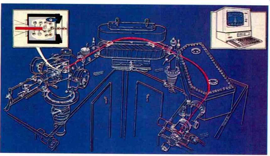
Fig. 1. The major components of the system: from left to right, glow discharge
source, analyzer and detector.
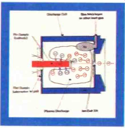
Fig. 2. Section through the glow discharge source.
PRINCIPAL COMPONENTS OF A GDMS SYSTEM
The system can be considered to consist of four major components, the glow discharge source, a mass analyzer, detector system and control computer as shown in Fig 1. The source produces a stream of ions which are subsequently separated on the basis of their mass to charge ratio by a double focusing mass spectrometer. Electronic detection of the ions is by a Faraday/Daly dual detector system.
Operation of the instrument is accomplished by a powerful PC-based system which also serves to acquire data and perform the data reduction and formatting.
The glow discharge source. The sample serves as a cathode in a low pressure (0.5m bar) argon plasma in a small tantalum discharge cell (the anode). The sample is inserted into the cell and several hundred volts potential applied between the sample (cathode) and the cell (anode) causing the breakdown of the argon gas to form a plasma. Argon ions impact upon the surface of the sample, resulting in the generation of sputtered neutral species of the sample atoms. Any positive ions produced are attracted back to the sample surface, whilst the neutral atoms diffuse into the central column of the plasma where they are subsequently ionized by collision with metastable argon atoms or electron impact. (Fig.2) The reaction with metastable argon atoms is termed Penning exchange, and leads to a uniform ionization sensitivity (within a factor of 3) over the periodic table; hence true multi-elemental analysis is attained even in the absence of calibration standards. The separation of the sputtering and ionization process has considerable benefits over direct ionization at the sample surface (e.g. secondary-iron mass spectrometry or laser-ionization mass spectrometry), giving a response almost totally independent of the matrix. Hence, the combined effect provides for a powerful no-standards analysis.
The mass analyzer. The output from the glow discharge source consists mainly of singly charged analyte ions, with some back ground of doubly charged ions and singly charged molecular species. These potentially interfering ions range from a few parts per billion to around 100 parts per million in concentration relative to the matrix.
To ensure that none of these potentially interfering ions cause problems, the mass analyzer of the VG 9000 is double focusing:
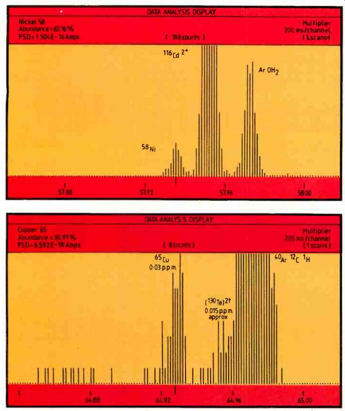
It consists of a combination of magnetic and electrostatic analyzers producing high re solution. Without this geometry, certain determinations would be background limited by the presence of one or more interfering ions. Figures 3 and 4 illustrate the analyzer’s ability to separate these species from the singly charged ion of analytical interest.
Thus, the molecular species, whilst they are obviously present, do not hamper the correct identification and determination of trace impurities. However, without a double-focusing geometry analyzer, a glow discharge source coupled to a low resolving-power (e.g. quadrupole mass filter analyzer) would be subject to background limitations at levels of a few p.p.m. and lower.
The detection system. The instrument uses a unique Faraday/Daly dual-detection system, having a combined linear dynamic range of more than 10 orders of magnitude. Since the Daly detector has a background of 1 count per second, p.p.b. concentration measurements are obtained in short integration times simply by direct ratio of the ion-beam intensity to the matrix. Typically, the Faraday is used to monitor the major components above 1000 p.p.m, whilst the Daly measures minor and trace components down to sub-p.p.b. concentration levels. Switching between the detectors is under computer control, enabling all measurements to be ratioed to the matrix signal in a single analytical cycle.
SAMPLE PREPARATION AND ANALYTICAL CONDITIONS
The g.d.m.s. source will accept conducting and semiconducting samples directly, with provision for accepting pelletized non conductors or powders. Surface contamination can be removed by a combination of chemical etching prior to loading the sample and pre-sputtering in the discharge cell. The rapid analysis and real-time data display enable the operator to track or profile compositional changes from the surface to the bulk of the material, as successive layers of material are sputtering away. In the normal bulk analysis mode of operation, this erosion rate is of the order of 1um/min, but adjustment of the source pressure enables this to be controlled down to around 0.1 um/min for quantitative depth profiling studies.
G.D.M.S. IN THE SEMICONDUCTOR INDUSTRY
Impurities in semiconductor materials can be classified into two categories, those deliberately introduced, as in the case of dopants such as boron or phosphorus, and those arising from impure raw materials or contamination from processing chemicals and equipment.
When studying the profile of a deliberately introduced dopant, it is essential to be able accurately to monitor the concentration of single elements (usually in the 1-40+ p.p.m. range). However, in the analysis for inadvertent contamination it is essential not only to maintain accuracy but also to do this across the entire periodic table. This comprehensive elemental coverage is a major advantage of g.d.m.s. over other techniques such as s.i.m.s., where not only is coverage much reduced but the sensitivity from element to element may vary by as much as three orders of magnitude. The other major technique for bulk analysis, spark source mass spectrometry (s.s.m.s.), is much slower in operation than g.d.m.s., shows less precision and provides inferior detection limits.
The capability of g.d.m.s. can be illustrated by a study of trace level determinations of transition elements in cadmium telluride, silicon and depth-profiling of gallium arsenide.
CADMIUM TELLURIDE
Cadmium telluride is used extensively in the electronics industry, either directly as a gamma-ray detector or as a raw material in the production of cadmium mercury telluride (CMT) which is used as an infra-red detector. In both these roles, the trace element composition is vital to the performance of the device and the transition element concentration is of particular importance.
The elements Fe, Ni and Cu have been difficult to determine by traditional techniques such as s.s.m.s. The reason for this is the high-level of doubly charged matrix ions (-10--20%) produced in s.s.m.s. Thus the Cd2+ and Te2+ peaks swamp the Fe, Ni and Cu peaks, making analysis difficult or impossible. A similar difficulty is seen with s.i.m.s., so that the effective limit of detection with this technique for these elements will be around the p.p.m. level.
Determination of trace levels of transition elements in cadmium telluride by g.d.m.s. is made practical due to the ionization process employed, which produces very low levels of doubly charged ions (typically <100 p.p.m. of the singly charged level) in combination with uniform element-relative sensitivity factors and small matrix effects.
Table 1 illustrates the results of g.d.m.s. in the determination of transition elements in the cadmium telluride sample as well as the concentration of the major components.
Element identification confirmation is illustrated by isotope ratio checks for Ni and Cu.
In general, detection limits of around 10 p.p.b. are obtained, based on 10 seconds integration time per peak.
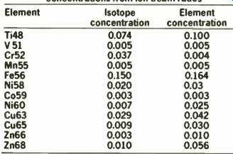
TABLE 1: Analysis of cadmium telluride by VG 9000 g.d.m.s. concentrations from
ion-beam ratios
Figures 3 and 4 illustrate the value of the excellent resolution obtainable by the high performance mass spectrometer. The element ions of 58Ni and 65Cu are clearly resolved from adjacent doubly charged species, oxides and other molecular species. In all cases it can be seen that the doubly charged species are less than 1 p.p.m. in concentration, thereby enabling precise identification and measurement of the transition metal isotopes at a nominal 4000 resolving power.
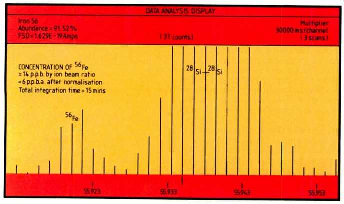
Fig. 5. Showing 56Fe at the 6p.p.b.a. level after normalization and the 28Si-28Si
dimer at the same nominal mass.
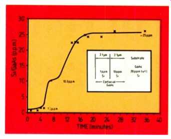
Fig. 6. Analysis of silicon surface films on GaAs substrate.
IRON AND OTHER TRANSITION METALS IN A SILICON MATRIX
In the analysis of a silicon matrix, a similar problem arises, as is shown with cadmium telluride, whereby transition elements can
be overlapped by neighboring species. In this case the problem is caused by the high relative concentration of the dimers (species formed by the union of two like atoms) of silicon 28, 29 and 30 at the same nominal mass as 56Fe, 58Ni and 60Ni, making analysis difficult by s.s.m.s and s.i.m.s.
In the analysis of silicon by g.d.m.s. the silicon dimers are at a level as low as 1 p.p.m. and when a resolution of 6000 is used it is more than adequate to resolve these dimers from the associated isotopes of interest.
Figure 5 shows 56Fe at the 6p.p.b.a. level after normalization, clearly resolved from the 28Si-28Si dimer at the same nominal mass; this was produced using an integration time of approximately 15 minutes.
Similar detection limits of a few p.p.b.a. parts per billion (atomic) have been achieved for other transition elements namely Cr, Mn, Co, Ni and Zn.
DEPTH PROFILING ANALYSIS
The controlled precise sputtering of the g.d.m.s. source enables both surface and bulk analysis of silicon. Table 2 shows the results of the analysis of another silicon sample where column 1 indicates the surface composition immediately after introduction and column 2 the bulk of the material after a period of sputter etching. This ability to determine trace composition at certain depth resolution in the sample is of consider-able interest and recent advances in the technique herald its increasing importance in depth profiling studies.
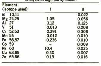
TABLE 2 Analysis of high purity silicon
All concentration parts per million:
Run I was acquired immediately after starting the discharge and is representative of the surface.
Run II was acquired after a sputter-etch period and is representative of the bulk of the sample.
The bulk analysis determinations de scribed above have been carried out using the standard pin sample configuration (15mm x 2mm diameter) and a pressure of around 0.5 to 1 tort of argon in the discharge cell. This results in an erosion rate of around 1 p.m per minute.
Using an alternative cell geometry, flat samples, for example semiconductor wafers around 10-25mm diameter, can be run directly. By reducing the argon pressure in the discharge cell the erosion rate can be controlled to below 0.1 µm per minute. This enables the analysis of thin surface films for impurity determinations and depth profiling analysis.
A sample of GaAs was doped with silicon in two epi-layers:
(a) at 1 ppm for a depth of 2.1 p.m;
(b) at 10 ppm for a further 2.1 p.m;
and (c) at 20 ppm approximately in the substrate.
The results in Fig. 6 show excel lent agreement between the VG 9000 and the quoted values.
CONCLUSIONS
Glow-discharge mass spectrometry possesses several unique properties and shows considerable benefits over other techniques for the analysis of semiconductor materials.
These major benefits are:
Full element coverage with approximately equal sensitivity for metals and non-metals
* Freedom from spectral interferences allowing determinations at trace levels which are impossible with other techniques
Excellent limits of detection (p.p.b.) Minimum matrix effects
Good semi-quantitative analysis without the need for standards
* Quantitative depth profiling.
This comprehensive range of attributes should see g.d.m.s. becoming more wide spread in both manufacturing processes and QA laboratories and it can be expected that further new applications will arise.
The authors are with VC Elemental--a division of VG Isotopes, Ltd.
==========
(adapted from: Wireless World , Oct. 1987)