By MARTIN GEORGE
This article looks at some of the areas that cause problems in analog circuit design, and urges that education gives more emphasis to training Britain's electronic engineers of the future in coping with them. With the help of low-cost, computer-aided design tools, this will help electronics companies compete successfully for business in many applications areas of increasing importance.
An understanding of fundamental analog design principles is vital to the design of cost-effective and reliable electronic circuits. In the final analysis, such understanding also has a significant effect on competitiveness of products designed, and therefore on profitability.
So much emphasis has been put on digital techniques in recent years, both in industry and in education, that 'analog' has almost become synonymous with 'obsolete'. Yet even digital circuits are affected by analog processes. For example, propagation delay is an analog effect.
UNDERSTANDING BEHAVIOR
A major obstacle to understanding the behavior of analog circuits is that they don't behave in black and white, or 1s and 0s.
They are distinctly grey with an infinite variety of shades, and with a highly inter dependent set of elements, any changes to which may have extensive ramifications in the final performance specification of the design.
Even relatively simple circuit designs need considerable work with a calculator, or a "design-by-soldering-iron" approach, wasteful of components and still not giving any real insight to prevent the same problems occurring again in the next design.
Expensive test and measuring equipment is then needed to check the design performance for gain and phase/frequency response, and input and output impedance at each stage. If designs that use integrated circuit building blocks such as operational amplifiers give rise to complex calculations of performance, those that use discrete components are positively fraught with traps for the unwary.
GREEN-FINGERED ELITE
There exists of course an elite of analog designers who seem to be able to bypass these problems, producing consistently effective analog circuit designs in many applications areas. Their 'green-fingered' experience has been hard fought for in the days when there was no alternative to the slog, but sadly that experience is not being replenished.
Help is at hand, though, because the complex matrix maths required to solve analog circuit design problems can be handled readily by any reasonable personal computer, and there are now some inexpensive programs on the market to assist and to help demonstrate the art of analog circuit design.
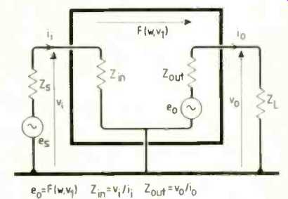
Fig.1. Block representation of circuit transfer function. Large circuits can
be broken down for analysis by chaining several such blocks, perhaps with a
simpler transfer function.
============
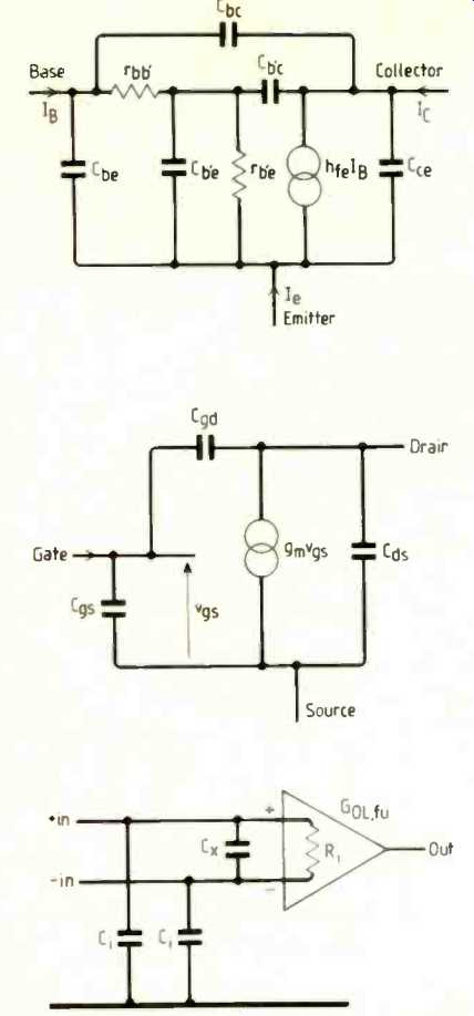
Fig. 2. Active component models used with in Analyzer. Hybrid-pi bipolar-transistor
model (a), field-effect-transistor model (b), and operational-amplifier model
(c).
COMPUTER-AIDED DESIGN AND THE ELECTRONICS ENGINEER
Computer-aided design was originally used to denote computer-controlled drawing systems and these could equally be used by any draughtsman to replace conventional drawing boards in architecture and mechanical engineering as well as electronics designs. Systems became specialized when they could store in memory regularly-used images of the elements used in specific systems so that an electronics circuit design drawing program would include images (icons) of transistors, capacitors, integrated circuits and the like. A PCB design program would include tracks of different widths and ions of connector pad patterns, such as dual-in-line or 'fingers' for edge connectors.
When 'intelligence' is introduced to such systems it is possible to connect separate programs. So that the system car translate the circuit diagram into a PCB pattern, or check that after such translation the correct components are connected.
Regularly used parts of circuits can be stored in a computer as 'macros' so that when another memory block, for instance, is needed it can he called up in its complete form and added to the circuit or layout. The next step is for a program to analyze a design and simulate its function. This can provide a full theoretical test which can indicate the operating speed, bandwidth or frequency response, without building the circuit at all Integrated-circuit designs also need rule-checking software to make sure that conductors are correctly spaced, and that components do not adversely affect each other by stray capacitance or inductance.
Simulation software needs to run a test pattern on the design to verify its function. Such patterns can also be used to generate a test program for the manufactured IC Various levels of design are needed for integrated circuits, from complete IC designs to metal overlays to connect ready-built cells in logic-array or application-specific IC’s.
With the emergence of 'fifth-generation' computers more of these processes are becoming integrated so that it becomes possible for a computer to design an IC in response to a list of required functions. Ultimately there could be the Hitchhikers Guide prediction of a computer that can design another computer better than itself!
============
FREQUENCY RESPONSE OF AC LINEAR CIRCUITS
In designing linear AC analog circuits, which make up the great majority of analogue applications, frequency response is the primary subject of interest, and in particular four parameters that vary with frequency (and other factors). These four are gain, phase, input impedance and output impedance.
Thus a design can be expressed as a circuit block with an input signal (voltage or current) and an output signal (voltage or current), whose transfer function (how the output signal varies with changes in the input signal) can be described in terms of these four parameters (see Fig.1). Note that the input signal will not be an ideal source, and any impedance associated with it must be taken into account by the circuit analysis.
The same applies for any impedance associated with the output load which the circuit drives.
The overall circuit block will almost certainly be too complex to analyze as a whole.
Traditional methods of design break it down into several simpler stages, which are manageable. This means that the interaction between the blocks caused by non-ideal input and output impedances of each stage must be minimized, usually by rule-of-thumb methods which ensure that the input impedance of one stage is 'very large' (e.g. a factor of 10 000) compared to the output impedance of the previous stage, at all frequencies. The result is that the overall design cannot really be optimized.
GAIN BLOCK OR DISCRETE COMPONENT DESIGN
So this technique is not ideal, and has encouraged designers to opt for gain (amplifier) blocks, which can be realised as ICs, in developing circuits. While more predictable, use of ICs does not necessarily encourage the most cost-effective or even the highest performance design, as evidenced by the intensive use of discretes in Far-East produced radios and hi-fi equipment. Indeed, for many high-frequency applications the use of discrete components may be the only way to design successfully, and in other applications too can result in a simpler design with lower component count and greater inherent reliability.
In any circuit block, the designer will normally set out to achieve a specific transfer function, such as in the case of a filter design, where, say, a peak in gain at a particular frequency is required, with gain falling away to below specified values at either side of the peak. The basic circuit design can be chosen from standard text book sources if required, leaving the designer to work out component values to meet the required performance.
DC CONDITIONS AND COMPONENT VALUES
Once the basic circuit design has been established, the really time-consuming pro cess of analysis and refining can begin.
If a standard textbook design has been chosen, component values can be calculated from formulae given to provide a first approximation of the required performance. In a design from scratch, the designer will have to use his own experience to calculate or estimate values from first principles or rule-of-thumb methods. Any components that affect DC conditions must first be set to satisfy these before calculating the values of other components, since all may interact to affect AC performance.
BREADBOARDING TO REFINE PERFORMANCE
Now the fun really starts! The next step is to breadboard the circuit, and apply suitable input signals from a test source that simulates as nearly as possible the impedance and signal level of the real-life source. Output signals are measured across a load that again simulates the real one (or using the real load if available).
Readings may also be taken with open circuit output, and with varying loads, to assess impedance. Tedious enough if you have a phase-meter and a decent AC milli-voltmeter, but with only an oscilloscope...
COMPUTER CIRCUIT-ANALYSIS TO THE RESCUE
Contrast this procedure with that required when using a computer-aided circuit design tool such as Analyzer, produced by Number One Systems Ltd., which runs on popular computers such as IBM compatibles, Re search Machines Nimbus and BBC.
The first stages of producing the basic circuit design are the same, and any required DC conditions in the circuit must be established. It will help, but it is not essential, to know a first approximation of the values of other passive components in the circuit.
Active components are entered from a library of types whose specifications (rbb, Cb’c, Cb’e, Cce., for bipolar transistors; Cg, Cgd, Cds and gm for fets; and Ri , fu, Gol, fu, Ci, and Cx for operational amplifiers) are held within the program, but which can be edited by the user to cope with different types.
Bipolar transistors use the well-proven hybrid-pi model, but a simpler model with just Cb’e is also available within Analyzer (Fig. 2).
NO NEED TO SPLIT UP COMPLEX CIRCUITS
Circuits will almost certainly not need to be broken up into smaller blocks, since Analyzer can cope with circuits containing up to 60 nodes and 180 components, immediately removing a source of error and allowing the designer to deal with highly complex circuits.
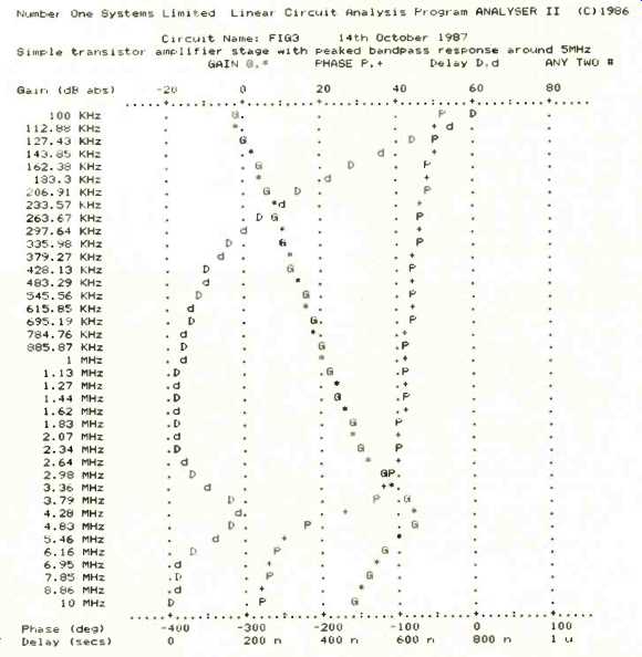
The circuit is labeled up by numbering all the node points where components inter connect, including the input node, the output node and the common node. Components are entered into Analyzer by specifying their identification number and type (e.g. R3, QB2, etc), the node numbers they connect to, and the component value (see Fig.3). In the case of bipolar transistors, the user specifies DC collector current Ic, and the gain hfe and transition frequency fT, of the transistor at this collector current. This method takes into account variations in performance of the device at differing collector currents.
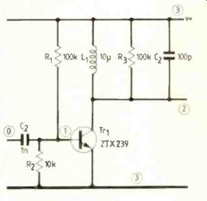
Fig. 3. Simple transistor amplifier with tuned output circuit. It has a peaked
band pass response with Fo around 5MHz (analysis example in the text) Note
the numbering of circuit nodes from 0 to 3, and for AC purposes, both supply
rails are treated as ground. Capacitance and resistance could be added to simulate
a more practical circuit.
ANALYSIS WITH TABULATED AND GRAPHIC RESULTS
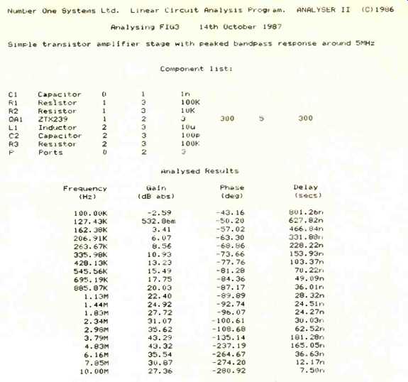
When all the components are entered, Analyzer gives a summary of the circuit so that correct entry of components can be checked.
At this point, analysis of the circuit can begin. The user has a choice of voltage gain and phase, or input impedance or output impedance analysis over any specified number of linear or logarithmic frequency steps.
Results can be calculated in real and imaginary (Cartesian) co-ordinates, or magnitude and angle (polar) forms. Values can be given as direct numeric or decibel (dB), absolute or relative to a specified reference value.
These calculated forms allow Analyzer to preset results in any convenient way, for example to show dB/decade response roll-off.
Calculation of group delay (rate of change of phase with frequency) is also available.
This parameter is very awkward to calculate manually, since it requires a second set of calculations at a slightly shifted frequency from the first set. It provides an important measure of the different delays in propagation of different frequencies in, for example, communications signal paths.
Analyzer first tabulates the calculated results on screen, and then allows options to print the results, to display them graphically on screen, and to print the graph. This graph shows the gain and phase (or impedance) performance of the circuit at a glance, and shows up, within a few tens of seconds of starting the analysis, if changes to the circuit design need to be made.
CHANGING COMPONENTS WITHOUT SOLDERING
Component changes can be entered by simply editing the necessary component(s) with in the component list. Re-evaluation of the circuit is a repeat of the first analysis, and is again completed within a few tens of seconds. This repetitive process to fine-tune a circuit to the required performance, or to show 'what if effects, can be followed from the engineer's or student's desk without the need to wield a soldering iron or oscilloscope probe in anger at any stage! Moreover, it can be done very quickly.
Not that I am advocating abandoning these worthy tools-the circuit design (if it is to become a real design) will need to be tested at some point. But the use of Analyzer will make it possible to test the circuit at a prototype PCB stage rather than through a tedious breadboard development process.
Because of Analyzer's clear and logical menu-driven operation, the user will quickly achieve this degree of confidence, eliminating the traditional rat's-nest problems of breadboarding. For education, the need for the soldering iron and measuring equipment is greatly reduced, since circuit simulation is all that is required for many teaching purposes. This will save a considerable amount out of tightly-squeezed teaching budgets.
Of course, you may still want to check that Analyzer's results do really mean what they say. Number One Systems tell me of a user al one particular University who entered a circuit from a text book to check up on Analyzer, only to discover that the textbook gave the wrong circuit analysis formulae!
HELP FOR THE HIGH FREQUENCY DESIGNER
Analyzer takes into account the effects of inter-electrode capacitances in bipolar and field-effect transistors, and input to input and ground capacitances in operational amplifiers. A parasitic capacitance of 0.2pF is added across resistors to allow for what is the case in practice. These hidden elements can affect circuit performance in ways that the designer may not realize without the aid of a tool such as Analyzer, especially at higher frequencies.
A recent revision allows designers to analyze circuits that contain microwave striplines and transmission lines, to make Analyzer an invaluable tool for the r.f. designer, whose job without such aids is a very difficult one.
FUN ON A LOW BUDGET
It is hoped that the use of cad tools such as Analyzer will encourage designers to rediscover the joys of designing with discrete components, and enable them to produce more cost-effective and reliable designs, in a shorter space of time. For students, and teachers of electronics, Analyzer should help dispel the mystique of AC circuit theory by allowing simple and obvious demonstrations of their behavior, and of the effects of changing each element in the circuit. And that can only be for the good of the British electronics industry!
Further information on Analyzer is available from Number One Systems Ltd., St. Ives. Cambs.
Martin George is a freelance consultant, interested in furthering the role of electronics and technical computing in British industry through the co-operation of industry and education.
==========
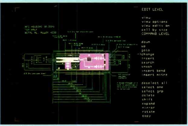
TeMCAD-MICROWAVE CIRCUIT LAYOUT
British Telecom has been exploring new circuit technologies which, unlike the traditional bulky and expensive waveguide, allow components to be built cheaply on circuit boards similar to the PCBs used at low frequencies. The requirements of high accuracy, fast turn-round, and easily modifiable designs demanded a cad process.
Such a cad tool for microwave applications would have to deal with little circuit complexity compared to, say, LSI design, but would need to deal with a wide range of the new circuit technologies such as microstrip and finline. It would therefore have to provide for instance microstrip track all of different widths, and curved taper sections for waveguide-to-finline transitions. Library designs would need to be such much more complex than simple pick-and-place because component topology varies non-linearly with parameters such as operating frequency and substrate material properties. Software should run on a laboratory PC rather than require an expensive workstation but nevertheless be powerful enough to be tailored to individual company practice.
TeMCAD was written to meet these needs. Most of the flexibility is in the cell library, which can be modified and added to by the user to meet his specific requirements. Because designs stored in the library can include the electrical design equations, the software is capable of handling a wide range of circuit technologies and microwave components. Even coordinate data can be entered in the form of a calculation, bypassing the stage where an engineer keeps a pocket calculator alongside the computer. The editing commands also have, with microwave use in mind, the ability to radius or mitre bends, rotate through arbitrary angles, include taper sections, and incorporate experimental data into component designs.
The system is used by BT in the design of radio systems operating in frequency bands up to 100GHz. Further details can be obtained from BT's Business operations division, Martlesham Research Laboratories, Ipswich.
==========
==========
(adapted from: Wireless World , Dec. 1987)