The digital system (also known as the binary system) is based on counting in 1's. Thus it has only two digits (known as "bits") -- 0 (zero) and 1 (one) -- which are very easy to manipulate electronically. It only needs a simple on-off switch, for example, to count in this manner. The switch is either "off" (showing zero as far as the circuit is concerned) or "on" (representing a count of 1). It can continue to count in l's, or even multiply, divide, etc, in association with other simple types of switches. The fast-as-light speed at which electronic devices can count makes the digital system very suitable for building computer circuits, particularly as only a few basic operations have to be performed. The fact that these operations, using simple logic circuits or gates in suitable combinations, may have to be repeated very many times is no problem either.
The decimal system expresses a number in powers of 10. In other words individual digits, depending on their order represent the digit value x 10°, digit value x 10, digit value x 10^2, etc, reading from right to left.
Putting this the correct way round, and taking an actual number--say 124:
124 = 1 x 10^2 + 2 x 10^1 + 4 x 10^0 = 100 + 20 + 4
The binary system expresses a number in powers of 2 using only the two digits 1 and 0.
Thus 1011 = 1 x 2^3 + 0 x 2^2 + 0 x 2^1 + 1 x 2°= 8 + 0 + 2 + 1= 11
Thus a binary number is longer, written down, than its corresponding decimal number, and can get very long indeed with large decimal numbers (e.g., 10,000 = 1010100010000) but this does not matter at all as far as electronics "counting" is concerned. It only makes it difficult for people to convert decimal numbers to binary numbers, and vice versa. Here are two basic rules.
CONVERTING DECIMAL TO BINARY
Write the decimal number on the right-hand side, divide by two and write down the result, placing the remainder (0 or 1) underneath this number. Divide the number obtained in the top line by 2 and carry the remainder (0 or 1) down to make a next step to the left. Repeat this operation, progressing further to the left each time, until you are left with a 0 in the top line. For example, convert the decimal number 19 to binary.
19/2 = 9, remainder 1, 9/2 = 4, remainder 1 4/2 = 2, remainder 0 2/2 = 1, remainder 0 1/2 = 0, remainder 1 Written as described above, we have: decimal numbers: 0 1 2 4 9 19 remainders: 1 0 0 1 1 and the remainders put together gives us the number 19 converted to binary, 10011.
CONVERTING BINARY TO DECIMAL
Write down progressively from right to left as many powers of 2 as there are digits in the binary number. Write the binary num be underneath. Determine the powers of 2 in each column where a 1 appears under the heading and then add all these up. Example Binary number 10101, which has 5 digits, so write down five stages of powers of 2 starting with 2° and reading from right to left.
Powers of two 2^4 2^3 2^2 2^1 2° Write down binary number 1 0 1 0 1 Convert to decimal 16 0 4 0 1 Add 16 + 4 + 1 = 21
LOGIC
Logic systems also work on the binary number process, commonly based on the difference between two dc voltage levels. If the more positive voltage signifies 1, then the system employs positive logic. If the more negative voltage signifies 1, then the system employs negative logic.
It should be noted that in both cases, al though the lower or higher voltage respectively signifies 0, this is not necessarily a zero voltage level, so the actual voltage values have no real significance.
There is another system, known as pulse-logic, where a "bit" is recognized by the presence or absence of a pulse (positive pulse in the case of a positive-logic system and negative pulse in the case of a negative-logic system).
GATES
Logic functions are performed by logic gates.
The three basic logic functions are OR, AND, and NOT. All are designed to accept two or more input signals and have a single output lead. The presence of a signal is signaled by 1 and the absence of a signal by 0.
The four possible states of an OR gate with two inputs (A and B) are shown in Fig. 1. There is an output signal whenever there is an input signal applied to input A OR input B (and also with in put at A and B simultaneously). This applies regardless of the actual number of inputs the gate is designed to accept.
The behavior of an OR gate (again written for only two inputs) is expressed by the following truth table:
A B output(Y)
0 0 0
0 1 1
1 0 1
1 1 1
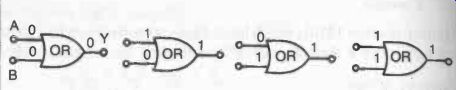
Fig. 1. The four states of an OR gate.
It can also be expressed in terms of Boolean algebra, calling the output Y Y=A+B+...+N where N is the number of gates The important thing to remember is that in Boolean algebra the sign + does not mean "plus" but OR.
The AND gate again has two or more inputs and one output, but this time the output is 1 only if all the inputs are also 1. The truth table in this case is quite different--Fig. 2. The corresponding equation of an AND gate is:
Y=AB...N or Y=AxB...xN
This time the or x sign does not mean "multiplied by" as in conventional arithmetic, but AND.
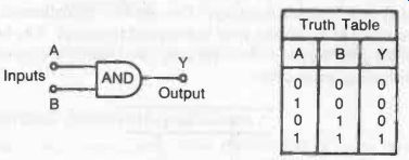
Fig. 2. An AND gate and corresponding truth table.
The NOT gate has a single input and a single output-Fig. 10-3, with output always opposite to the input, i.e., if A = 1, Y = 0 and if A = 0, Y = 1.
In other words it inverts the sense of the output with respect to the input and is thus commonly called an inverter.
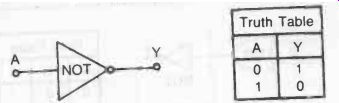
Fig. 3. A NOT gate and corresponding truth table.
Its Boolean equation is:
Y = (Y equals NOT A)
Inverting the output of an AND gate gives us a NAND (Not AND) gate. A NAND gate is illustrated in Fig. 10-4. It is just the opposite of an AND gate. The output of a NAND gate is 0 if, and only if, both of the inputs are 1's.
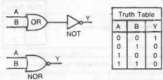
Similarly, inverting the output of an OR gate results in a NOR gate, as shown
in Fig. 5.
Another variation on the OR gate is the XOR (eXclusive OR) gate, which is illustrated in Fig. 6.
The output is a 1 when only one of the inputs is a 1. This gate could also be considered a logical difference detector. If the two inputs are equal, the output is 0. If the inputs are at different logic levels, the output will be a 1.
Diode-logic (DL) circuits for an OR gate and an AND gate are shown in Fig. 7.
Both are shown for negative logic and are identical except for the polarity of the diodes. In fact, a positive-logic DL or OR gate becomes a negative-logic AND gate; and a positive-logic AND gate a negative-logic OR gate.
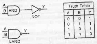
Fig. 4. Inverting the output of an AND gate creates a NAND gate.
Fig. 5. Inverting the output of an OR gate creates a NOR gate.
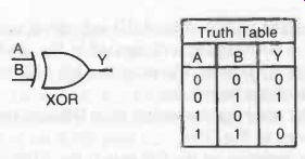
Fig. 6. A variation on the basic OR gate is the XOR (eXclusive OR) gate.
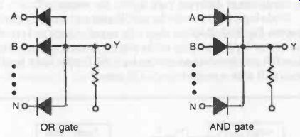
Fig. 7. A Diode Logic (DL) negative logic OR circuit (left) and a DL negative
logic AND gate (right).
The simple NOT gate or inverter shown in Fig. 10-8 is based on a transistor logic-an NPN transistor for positive-logic and a PNP transistor for negative-logic. The capacitor across the input resistance is added to improve the transient response.
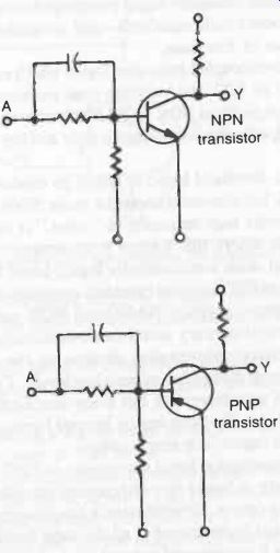
Fig. 8. Transistor Logic (TL) positive logic inverter circuit (top) and
a TL negative logic NOT circuit (bottom).
PRACTICAL GATES
Most logic gates are produced in the form of integrated circuits, from which various "family" names are derived. NAND and NOR gates, for example, are a combination of AND or, OR gates, respectively, with a NOT gate inverter. From the basic circuits just described, such functions can be performed by diode-transistor logic or DTL gates.
Faster and better performance can be realized with transistor-transistor-logic gates (TTL). During the early 1970's DTL and TTL represented the bulk of the IC digital productions, but since then various other IC families have appeared, each offering specific advantages and more functions for particular applications. These are:
RTL (resistor-transistor logic) which can be made very small even by microelectronic standards-and is capable of performing a large number of functions.
DCTL (direct-coupled-transistor logic), which employs the same type of circuit as RTL but with the base resistors omitted. This gate, which can perform NOR or NAND functions, has the advantage of needing only one low voltage supply and has low-power classification.
HTL (high threshold logic) is based on diode-transistor logic similar to DTL but also incorporates a zener diode to stabilize the circuit and provide high immunity to "noise." It is usually chosen for applications where this feature is important.
MOS (metal oxide semiconductor logic), based entirely on field effect transistors (FETs) to the complete exclusion of diodes, resistors and capacitors, yielding NAND and NOR gates.
CMOS (complementary metal-oxide-semiconductor logic) using complementary enhancement devices on the same IC chip, reducing the power dissipation to very low levels. The basic CMOS circuit is a NOT gate (inverter), but more complicated NAND and NOR gates and also flip-flops can be formed from combinations of smaller circuits (again in a single chip).
ECL (emitter-coupled logic) also known as CML (current-mode logic). This family is based on a differential amplifier which is basically an analog device. Nevertheless it has important application in digital logic and is the fastest of all the logic families with delay times as low as 1 nanosecond per gate.
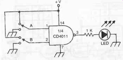
Fig. 9. This simple circuit demonstrates the operation of a NAND gate.
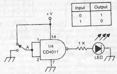
Fig. 10. Tying the inputs of a NAND gate together creates an inverter.
GATE DEMONSTRATION CIRCUITS
To give you a better understanding of how digital gates work, we will present several demonstration circuits built around the CD4011 quad NAND gate. Any digital gate can be constructed from NAND gates.
In Fig. 9 we have the basic NAND circuit. The LED will be lit (logic 1) if one or both inputs (A or B) are grounded (logic 0). If both of the switches is moved to the + V line (logic 1), the LED will be dark (logic 0).
By shorting the two inputs together into a single input line, as shown in Fig. 10 we have a simple inverter demonstrator. If the input is logic 1 (V + ), the output will be logic 0 (LED dark). If the input is logic 0 (ground), then the output will be logic 1 (LED lit). Inverting the output of a NAND gate produces an AND gate.
This can be done with two NAND gate stages, as illustrated in Fig. 11.
On the other hand, inverting the inputs of a NAND gate simulates an OR gate. A demonstration circuit for this is shown in Fig. 12.
Simply adding a fourth stage (as an inverter) creates a NOR gate, as illustrated in Fig. 13.
A number of non-standard gating schemes can also be created.
For example, the circuit shown in Fig. 10-14 is a combined AND/OR gate. The output is a logic 1 if A and B are 1's or C and D are 1's.
If all four inputs are l's, the output will also be a 1.
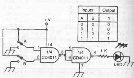
Fig. 11. An AND gate can be built from two NAND gate stages.
Fig. 12. This circuit demonstrates how an OR gate can be created from three NAND gates.
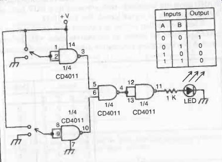
Fig. 13. Adding an inverter stage to the OR gate circuit of Fig. 10-12
turns it into a NOR gate.
Digital gates can be used for more than simple logic switching applications. The circuit in Fig. 10-15 is a simple low frequency square wave oscillator. When the input is a logic 1 (connected to V + ), the circuit will oscillate. The LED will blink on and off once or twice a second. A logic 0 at the input (grounded) disables the oscillator.
Try different capacitor values to create other frequencies. If the frequency is too high, the eye will not be able to distinguish between the separate blinks. The LED will appear to stay continuously lit when the oscillator is enabled.
Try routing the output to a small speaker when using a smaller capacitor. (A 0.1 µF capacitor would be a good choice.) You will hear a tone from the speaker when the oscillator is enabled.
FLIP-FLOPS
A flip-flop is a bistable circuit and another important element in digital logic. Since it is capable of storing one bit of information it is functionally a 1-bit memory unit. Because this information is locked or "latched" in place, a flip-flop is also known as a latch.
A combination of n flip-flops can thus store an n-bit word, such a unit being referred to as a register.
A basic flip-flop circuit is formed by cross-coupling two NOT gates, the output of each gate being connected back to the input of the other gate. The NOT gates can be created from NAND gates as described earlier, and the final circuit will look like Fig. 16.
However, to be able to preset or clear the state of the flip-flop, two NAND gates are necessary, each preceded by a NOT gate, or a NAND gate with its inputs joined. See Fig. 17.
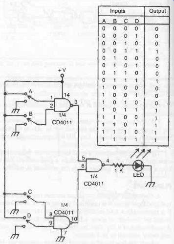
Fig. 14. This circuit demonstrates how basic gates can be combined into
non-standard gating arrangements.
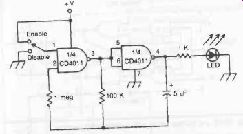
Fig. 15. Digital gates can be used for more than just simple switching
circuits. This is a gated digital square wave oscillator.
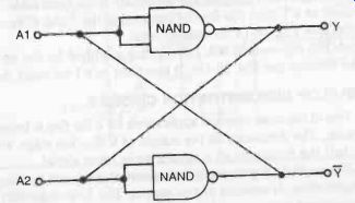
Fig. 16. A 1 bit memory or latch circuit is obtained by cross-coupling
two NOT gates, or two NAND gates with their inputs shorted.
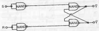
Fig. 17. Flip-flop circuit with preset using four NOT gates.
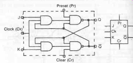
Fig. 18. J-K flip-flop circuit with corresponding symbol.
When the flip-flop is used in a pulsed or clocked system the preceding gates are known as the steering gates with the cross-coupled two-input gates forming the latch. This particular configuration is also known as a S-R or R-S flip-flop. Two other variations of the flip-flop are also produced as integrated circuits:
PK flip-flop-which is an S-R flip-flop preceded by two AND gates.
This configuration removes any ambiguity in the truth table. It can be used as a T-type flip-flop by connecting the J and K inputs together (see Fig. 18 for connections).
D-type flip-flop-which is a J-K flip-flop modified by the addition of an inverter (see Fig. 19). It functions as a 1-bit delay device.
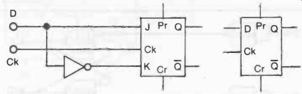
Fig. 19. A D-type flip-flop circuit is provided by a J-K flip-flop allied
with an inverter.
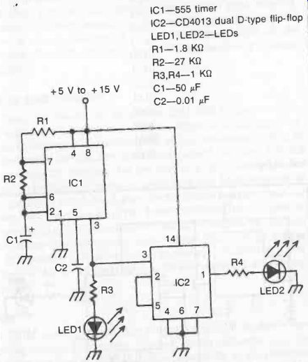
Fig. 20. This circuit demonstrates how a flip-flop can be used for frequency
division.
FLIP-FLOP DEMONSTRATION CIRCUITS
One of the most common applications for a flip-flop is frequency division. The frequency at the output of a flip-flop stage will be one half the frequency of a square wave input signal.
Figure 10-20 shows a simple demonstration circuit for this type of application. It consists of two stages. The first stage (IC1 and its associated components) is a simple 555 astable multivibrator (see Section 7). With the component values listed, it will produce a near square wave with a frequency of about 1 Hz. The second stage (IC2) is one half a dual D type flip-flop IC (CD4013). The frequency is divided by two in this stage.
LED1 will blink on and off approximately once a second, while LED2 (the output) will blink once every other time LED1 (the in put) blinks.
Any number of flip-flop stages can be strung together. By looking at each stage output, a binary counter can be created. A simple modulo-8 counter circuit is shown in Fig. 21. This circuit will count from 0 (0000) to 8 (1000), then cycle back to 0 and start over. That is:
0001
0010
0011
0100
0101
0110
0111
1000
0000
0001
0010
… and so forth.
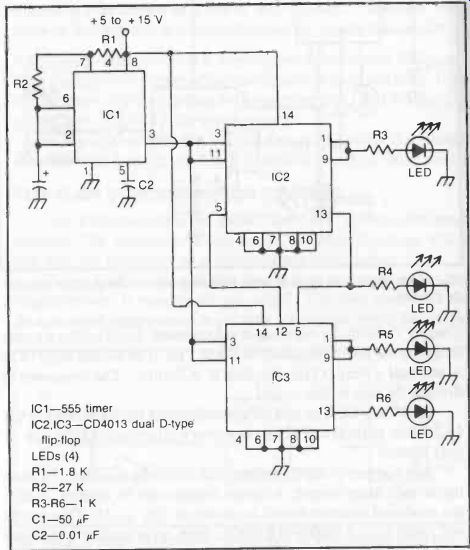
Fig. 21. Flip-flop stages can be combined to create binary counters.
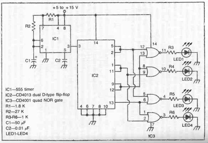
Fig. 22
See Fig. 22. Here only one LED will be lit (logic 1) at any given moment.
The circuit will step through the four outputs repeatedly, activating one at a time. This type of circuit is sometimes called a 1-of-4 sequencer.
It can be extended to include as many output stages as desired.
FAN-IN AND FAN-OUT
The terms fan-in and fan-out are used with IC logic devices.
Fan-in refers to the number of separate inputs to a logic gate. Fan-out is the number of circuit loads the output can accommodate, or in other words the number of separate outputs provided. Fan-out is commonly 10, meaning that the output of the gate can be connected to 10 standard inputs on matching gates.
Each separate in put represents a load, the higher the number of separate loads the higher the current output of the device providing fan-out needs to be in order to provide the standard load on each input, i.e., passing enough current to drop each input voltage to the design figure.
It is possible to increase fan-out by replacing diode(s) with transistor(s) in the device concerned, so 10 is by no means a maximum number.
ROM
ROM stands for Read-Only-Memory, a system capable of converting one code into another. The best known application is to convert the reading of a digital instrument such as an electronic calculator into a numerical read-out via an LED (light emitting di ode) display. The advantage of a ROM is that it is programmable and thus adaptable to different read-out systems.
It does not follow, however, that it uses the minimum number of components to match a particular application.
Special IC chips designed for a specific application may be more economic in this respect, but not necessarily in cost, unless there is a very large demand for that particular IC. The calculator market is a case in point where a special chip can offer advantages over a ROM.
RAM
RAM stands for Random-Access Memory and is basically a collection of flip-flops or similar devices capable of memorizing information in binary form.
Information can be written-in or read out in a random manner.
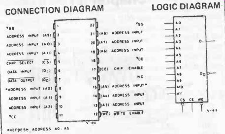
Fig. 23. Example of a Random Access Memory integrated circuit with connection
diagram.
THE SHAPE OF DIGITAL ICs
In physical appearance, most digital ICs look like any other dual in-line (or sometimes quad in-line) IC package, or ceramic flat pack ages. They are not readily identified as digital ICs, therefore, (except by type number) although their function is quite specific. The more complicated digital ICs may, however, have considerably more pins than usual. It is also common practice to give pin dia grams which not only define the pin positions but also their specific function (Fig. 23).