Op-amps (operational amplifiers) are a particular class of integrated circuit comprising a directly-coupled high-gain amplifier with overall response characteristics controlled by feedback. The op-amp gets its name from the fact that it can be made to perform numerous mathematical operations. An op-amp is the basic building block in many analog systems and is also known as a linear integrated circuit because of its response.
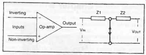
Fig. 1. A basic op-amp is a three terminal device with the corresponding
circuit as shown.
It has an extremely high gain (theoretically approaching infinity), the actual value of which can be set by the feedback. The introduction of capacitors or inductors in the feedback network can give gain varying with frequency and thus determine the operating condition of the whole integrated circuit.
The basic op-amp is a three-terminal device with two inputs and one output--Fig. 1. The input terminals are described as "inverting" and "non-inverting." At the input there is a virtual "short circuit," although the feedback keeps the voltage across these points at zero so that no current flows across the "short." The simple circuit equivalent is also shown in Fig. 1, when the voltage gain is given by a ratio of the impedances Z2/Z1.
OP-AMP PARAMETERS
The ideal op-amp is perfectly balanced so that if fed with equal inputs, output is zero, i.e. VIN 1 = VIN 2 gives VOUT = 0
In a practical op-amp the input is not perfectly balanced so that unequal bias currents flow through the input terminal. Thus an in put offset voltage must be applied between the two input terminals to balance the amplifier output.
The input bias current (IB) is one half the sum of the separate currents entering the two input terminals when the output is balanced, i.e., V_OUT = 0. It is usually a small value, e.g., a typical value is 1B = 100 nA.
The input offset current (I_io) is the difference between the separate currents entering the input terminals. Again it is usually of a very small order, e.g., a typical value is I_io = 10 nA.
The input offset voltage V_io is a voltage which must be applied across the input terminal, to balance the amplifier. Typical value, V_io = 1 mV.
Both I_io and V_io. are subject to change with temperature, this change being known as I_Iio drift and V_io. drift, respectively.
The Power Supply Rejection Ratio (PSRR) is the ratio of the change in input offset voltage to the corresponding change in one power supply voltage. Typically this is of the order of 10- 20 µV /V.
Other parameters which may be quoted for op-amps are:
Open-loop gain-usually designated A_d.
Common-mode rejection ratio-designated CMRR. This is the ratio of the difference signal to the common-mode signal and represents a figure of merit for a differential amplifier. This ratio is expressed in decibels (dB).
Slew rate-or the rate of change of amplifier output voltage under large-signal conditions. It is expressed in terms of V/uS.
Some examples of the versatility of the op-amp are given in the following simple circuits:
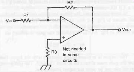
Fig. 2. One of the most basic of op-amp circuits is the inverting amplifier.
AMPLIFIER OR BUFFER
Figure 2 shows the circuit for an inverting amplifier, or inverter. The gain is equal to:
Av =- R2/R1
Notice that if the two resistances are equal (i.e., R1 = R2), the gain is negative one, meaning that the circuit works as a phase inverting voltage follower. The output will be the same as the input, except the polarity will be reversed.
In fact, for unity gain, the resistors can be eliminated and re placed with direct connections, as illustrated in Fig. 3. This works because in this circuit R1 = R2 = 0. R3 is usually eliminated in the inverting voltage follower circuit.
If R1 is smaller than R2, the input signal will be amplified at the output. For example, if R1 is 2.2 K-O and R1 is 22 K-o, the gain will be:
Av =- 22,000/2,200 =-10
The minus sign indicates phase inversion. The output polarity is reversed from the input.
The same circuit can also attenuate (reduce the level of) the input signal by making R1 larger than R2. For example, if R1 is 120 K-o, and R2 is 47 K-O, the circuit gain will be approximately:
Av = 47,000/120,000 =- 0.4
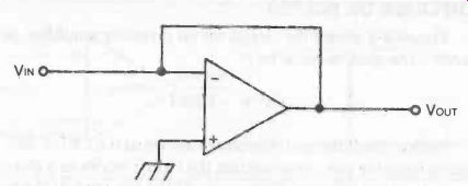
Fig. 3. If the input and feedback resistors are eliminated, the gain of
an inverting amplifier will be 1.
Once again, the output's polarity is the opposite of the input's polarity.
The value of R3 is not terribly critical, but it should be approximately equal to the parallel combination of R1 and R2. That is:
R3 = (R1 x R2)/(R1 + R2)
To illustrate this, let's return to our earlier example, in which R1 = 2.2 KO and R2 = 22 KO. In this case, the value of R3 should be about:
R3 = (2200 x 22000)/(2200 + 22000) = 48,400,000/24,200 = 2000 ohm
Since the exact value is not critical, we can use the nearest standard resistance value for R3. In this example, either a 1.8 K-O or a 2.2 K-o resistor may be used.
In some applications, the phase inversion produced by the circuit shown in Fig. 2 may be undesirable. To have the op-amp work as a non-inverting amplifier (buffer), the connections are made as shown in Fig. 4. In this circuit, the gain is defined as:
Av = 1 + R2/R1
The output is in phase (same polarity) with the input. Notice that the gain must always be at least 1 (unity). The non-inverting circuit can not be used for signal attenuation.
If R2 is considerably larger than R1, the gain will be relatively large. […] gain works out to:
Av = 1 + 470,000/10,000 = 1 + 47 = 48
If, on the other hand, R1 is considerably larger than R2, the gain will be just slightly greater than unity. For instance, if R1 = 100 K ohm and R2 = 22 K-O the gain will be:
Av = 1 + 22,000/100,000 = 1 + 0.22 = 1.22
If the two resistances are equal (R1 = R2), the gain will al ways be 2. Try a few examples using the gain equation to prove this to yourself.
A special case is when both resistances are made equal to 0.
That is, the resistors are replaced by direct connections, as shown in Fig. 5. Here, the gain is exactly unity.
This is in keeping with the gain formula:
Av = 1 + R2/R1 = 1 + 0/0 = 1 + 0 = 1
The output is identical to the input. This non-inverting voltage follower circuit is used for buffer, isolation, and impedance matching applications.
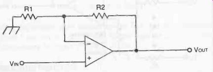
Fig. 4. An op-amp can also be used as a non-inverting amplifier.
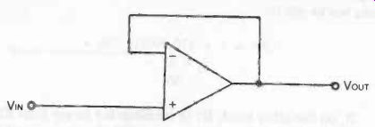
Fig. 5. A unity gain non-inverting amplifier can be used for buffer applications.
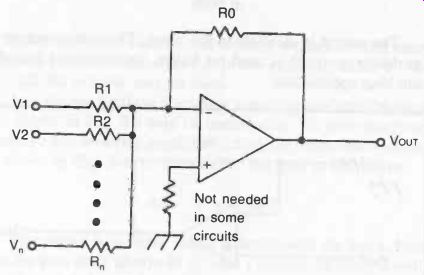
Fig. 6. Adder circuit based on an op
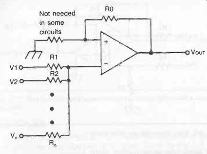
Fig. 7. Non-inverting adder circuit, i.e., the input and output have the
same polarity of signal and are thus in phase.
ADDER
An op-amp can be used to add multiple input voltages. Input signals V1, V2, . .. Vn are applied to the op-amp through resistors R1, R2, . .. Rn, as shown in Fig. 6. The output signal is then a combination of these signals, giving the sum of the inputs.
The actual performance of the op-amp as an adder can be calculated with this formula:
VOUT =- Ro ((V1/R1) + (V2/R2) . . . + (Vn/Rn))
Note the minus sign. This indicates that the output is inverted (the polarity is reversed). That is, this circuit is an inverting adder.
By changing the connections to the inverting and non-inverting inputs of the op-amp, as shown in Fig. 7, the circuit can be converted to a non-inverting adder.
If all of the input resistors have equal values, the output equation can be simplified to:
VOUT =- Ro ((V1 + V2 . . . + Vn)/R)
DIFFERENTIAL AMPLIFIER
A basic circuit for a differential amplifier is shown in Fig. 8.
Component values are chosen so that R1 = R2 and R3 = R4. Performance is then given by:
V_OUT = V_IN 2- V_IN 1
Provided the op-amp used can accept the fact that the impedance for input 1 and input 2 is different (impedance for input 1 = R1; and impedance for input 2 = R1 + R3).
ADDER/SUBTRACTOR
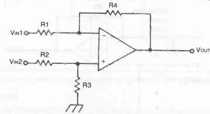
Fig. 8. Basic differential amplifier circuit.
Connections for an adder/subtractor circuit are shown in Fig. 9. If R1 and R2 are the same value; and R3 and R4 are also made the same value as each other, then:
V_OUT = V3 + V4- V1- V2 In other words, inputs to V3 and V4 give a summed output (V_out = V3 + V4). Inputs V1 and V2 subtract from the output voltage.
Values for R1, R2, and R3 and R4 are chosen to suit the opamp characteristics. R5 should be the same value as R3 and R4; and R6 should be the same value as R1 and R2.
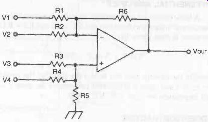
Fig. 9. Adder/subtractor circuit. See text for calculation of component
values.
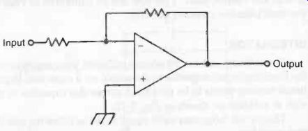
Fig. 10. This circuit is used to perform simple multiplication with a constant
multiplier.
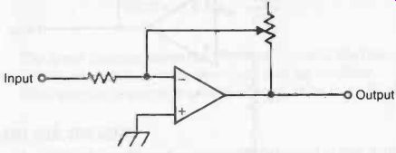
Fig. 11. Using a potentiometer as the feedback resistor allows the circuit
to be used with a variable multiplier.
MULTIPLIER
The circuit shown in Fig. 10 can be used to perform simple multiplication. Note that this is the same circuit as Fig. 2. For accurate results, precision resistors of the specified values for R1 and R2 should be used to give a constant gain (and thus multiplication of input voltage in the ratio R2/R1). Note that this circuit inverts the phase of the output.
The output voltage will be equal to:
VOUT =- (VIN x Av)
...where VOUT is the output voltage, VIN is the input voltage, and Av is the gain as defined by R1 and R2.
If a variable resistance (potentiometer) is used for R2, as shown in Fig. 11, the multiplication constant can be varied. A calibration dial with markings for various typical gains should be placed around the control shaft. This dial can be calibrated to read out the multiplication constant directly.
INTEGRATOR
Theoretically, at least, an op-amp will work as an integrator with the inverting input connected to the output via a capacitor. In practice, a resistor needs to be paralleled across this capacitor to provide de stability as shown in Fig. 12.
This circuit integrates input signal with the following relation ship applying:
VOUT- R1 1 C J VIN dt
* The value of R2 should be chosen to match the op-amp characteristics so that:
VOUT = R2 VIN R1
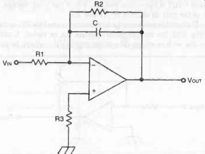
Fig. 12. Op-amp integrator circuit.
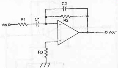
Fig. 13. Practical circuit for an op-amp differentiator.
DIFFERENTIATOR
The differentiator circuit has a capacitor in the input line connecting to the inverting input, and a resistor connecting this input to output. Again this circuit has practical limitations, so a better configuration is to parallel the resistor with a capacitor as shown in Fig. 13.
The performance of this circuit is given by:
VOUT =- R2 C1 dVIN dt
LOG AMPLIFIERS
The basic circuit (Fig. 14) uses an NPN transistor in conjunction with an op-amp to produce an output proportional to the log of the input:
VOUT =-k log 10 VIN RI.
The lower diagram shows the "inverted" circuit, this time using a PNP transistor, to work as a basic anti-log amplifier.
The capacitor required is usually of small value (e.g., 20 pF).
LOG MULTIPLIERS
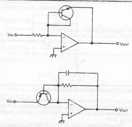
Fig. 14. Basic log amplifier circuits using a transistor in conjunction
with an op-amp.
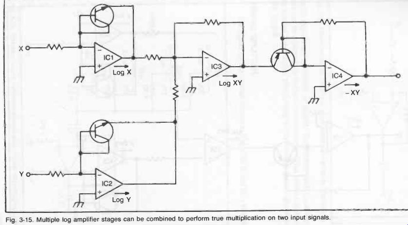
Fig. 15
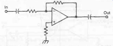
Fig. 17. Op-amps can be used for ac applications, as well as dc applications.
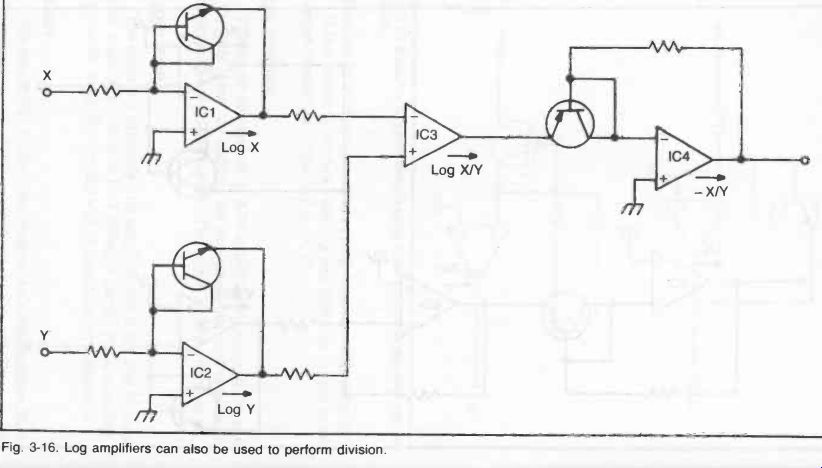
Fig. 16
Fig. 18. This mixer circuit combines multiple audio inputs into a single
output.
Fig. 19. A signal splitter is just the opposite of a mixer.
Logarithmic working of an op-amp is extended in Fig. 15 to give a log multiplier. Input X to one log amplifier gives log X output; and input Y to the second log amplifier gives log Y output.
These are fed as inputs to a third op-amp to give an output log X Y.
If this output is fed to an anti-log amplifier, the output is the inverted product of X and Y (i.e., X. Y).
LOG DIVIDER
The circuit shown in Fig. 16 is just the opposite of the one in Fig. 15. Here log and anti-log amp stages are used to perform division on the two input signals. The output is proportional to x/y.
AUDIO AMP
The op-amp is primarily a dc amplifier, but it can also be used for ac applications. Figure 3-17 shows a simple audio amplifier.
More audio amplifier circuits will be presented in Section 4.
MIXER
This circuit (Fig. 18) is a variation on the audio amplifier. Note the similarity to the adder circuit shown in Fig. 6. The various input signals are combined, or mixed. The level of each input signal can be adjusted via its input potentiometer. This allows the user to control the relative proportions of the various input signals in the output.
SIGNAL SPLITTER
The signal splitter circuit shown in Fig. 19 is just the reverse of a mixer. A single output signal is split off into multiple identical outputs to feed different inputs. This circuit is used to isolate the various signal paths from each other. Each output line has its own individual potentiometer to set the desired level.
VOLTAGE-TO-CURRENT CONVERTER
The circuit configuration shown in Fig. 20 will result in the same current flowing through R1 and the load impedance R2, the value of this current being independent of the load and proportional to the signal voltage, although it will be of relatively low value be cause of the high input resistance presented by the non-inverting terminal. The value of this current is directly proportional to VIN/R1.
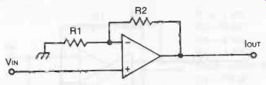
Fig. 20. Voltage-to-current converter using an op-amp.
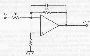
Fig. 21. Current-to-voltage converter using an op-amp.
CURRENT-TO-VOLTAGE CONVERTER
This configuration (Fig. 21) enables the input signal current to flow directly through the feedback resistor R2 when the output voltage is equal to IIN x R2. In other words, input current is converted into a proportional output voltage. No current flows through R2, the lower limit of current flow being established by the bias circuit generated at the inverting input.
A capacitor may be added to this circuit, as shown in the dia gram, to reduce "noise."
CURRENT SOURCE
Use of an op-amp as a current source is shown in Fig. 22.
Resistor values are selected as follows:
R1 = R2 R3 = R4 + R5
Current output is given by:
IOUT R3 VIN R1 R5
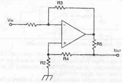
Fig. 22. Circuit for using an op-amp as a current source. See text for component
values required.
MULTIVIBRATOR
An op-amp can be made to work as a multivibrator. Two basic circuits are shown in Fig. 23. The one on the top left is a free running (astable) multivibrator, the frequency of which is determined by:
f- 1 2C R1 loge 2R3 + 1 R2
The lower right hand diagram shows a monostable multivibrator circuit which can be triggered by a square wave pulse input.
Component values given are for a CA741 op-amp. See also separate section on "Multivibrators."
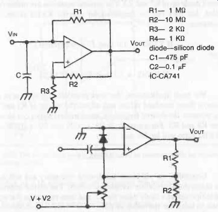
Fig. 23. Two basic circuits for a multivibrator, based on op-amps.
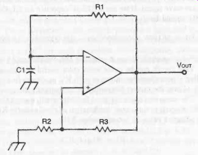
Fig. 24. This is perhaps the simplest possible square wave generator circuit.
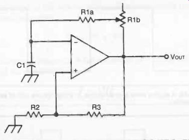
Fig. 25. The basic square wave generator can be adapted easily for variable
frequency output.
SQUARE WAVE GENERATOR
A practical square wave generator circuit built around an op-amp is shown in Fig. 24. This is perhaps the simplest possible square wave generator circuit. Besides the op-amp itself, only three external resistors and a single capacitor are required.
Resistor R1 and capacitor C1 are the primary components in defining the time constant (output frequency) of the circuit. But the output frequency is also affected by the positive feedback net-work made up of R2 and R3. The general equations are rather complex, but they can be simplified for specific R3/R2 ratios. For instance:
or:
If R3/R2 = 1.0 then F .--..- 0.5/(R1/C1)
If R3/R2 . 10 then F . 5/(R1/C1)
For most applications, the most practical approach is to use one of these standard ratios, and adjust the values of R1 and C1 to generate the desired frequency. Standardized values can be used for R2 and R3. For example, if R2 = 10K and R3 = 100K, the R3/R2 ratio will be 10, so:
F = 5/(R1/C1)
Generally, we will know the desired frequency and will need to select the appropriate component values. The easiest approach is to first select a likely value for C1, and then rearrange the equation to solve for the value of R1:
R1 = 5/(FC1)
Let's try a typical example. We want to generate a 1200 Hz square wave signal. If we use a 0.22 µF capacitor for C1, the value of R1 should be:
R1 = 5/(1200 x 0.00000022) = 5/0.000264 = 18,940 it
For most applications, a standard 18K resistor could be used.
This circuit can be made even more useful and versatile by adding a potentiometer in series with R1, as shown in Fig. 25.
This allows the output frequency to be manually changed.
The same equations are used for this circuit, except the value of R1 is equal to the series combination of fixed resistor R1a, and the adjusted value of potentiometer R1b;
R1 = R1a + R1b
The fixed resistor is included to prevent the value of R1 from ever becoming zero. The fixed value of R1a and the maximum resistance of R 1b sets the range of output frequencies.
VARIABLE PULSE WIDTH GENERATOR
A square wave is perfectly symmetrical. That is, it is in its high state for exactly one half of each cycle, as illustrated in Fig. 26.
The ratio of the high level time to the total cycle time is called the duty cycle of the signal. The duty cycle of a square wave is, by definition, 1:2.
Closely related to square waves are rectangle waves and pulse waves. These waveforms also switch between a high and a low state, but have different duty cycles. The terms "rectangle wave" and "pulse wave" are used somewhat interchangeably, although usually, a pulse wave is considered to have a relatively short high level time.
Figure 27 shows a rectangle wave with a duty cycle of 1:3.
The output level is high for one third of each cycle. The rectangle wave illustrated in Fig. 28 has a duty cycle of 1:4.
We can convert the square-wave generator described in the preceding section into a rectangle wave generator by adding just two components. The revised circuit is shown in Fig. 29.
On negative half-cycles, diode D1 blocks flow of current through R4. The time constant is comprised of R1 and C1:
T1 = 5/(2C1 R1)
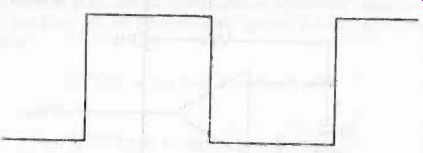
Fig. 26. A square wave is symmetrical. It is high for one half of each complete
cycle.
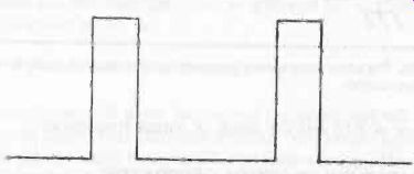
Fig. 27. A rectangle wave with a 1:3 duty cycle is high for one third of
each complete cycle.

Fig. 28. A rectangle wave with a 1:4 duty cycle is high for one fourth of
each complete cycle.
On positive half-cycles, however, the diode conducts and the time constant is defined by C1 and the parallel combination of R1 and R4:
T2 = 5/(201 ((R1 R4)/(R1 + R4)))
The length of the total cycle is simply the sum of the two half-cycle time constants:
Tt = T1 + T2
The output frequency is the reciprocal of the total time constant of the complete cycle:
F = 1/Tt
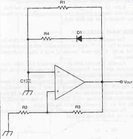
Fig. 29. This circuit generates asymmetrical rectangle waves
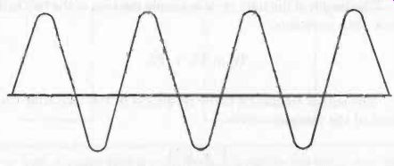
Fig. 30. The sine wave is the simplest ac signal.
Since the time constant will be different for the high and low level portions of the cycle, the duty cycle will be something other than 1:2. The output waveform becomes asymmetrical.
Either R1 or R4, or both, may be made variable, but bear in mind that changing either of these resistances affects both the output frequency and the duty cycle.
SINE WAVE OSCILLATOR
The simplest of all ac signals is the sine wave, which is illustrated in Fig. 30. This is a very pure signal with no harmonic con tent at all. A sine wave consists of only a single fundamental frequency.
Actually, it is quite difficult to generate a truly pure, distortion free, sine wave. Fortunately, we can come close to the ideal with an oscillator circuit built around an op-amp.
A typical sine wave oscillator circuit using an op-amp is shown in Fig. 31. The feedback network is a twin-T circuit, which functions as a band-reject (or notch) Filter. Resistors R1 and R2 along with capacitor C1 form one T. The other T is made up of C2, C3, R3, and R4. It is upside down in the schematic.
For this circuit to function properly, the component values must have the following relationships:
R2 = R1
R3 = R1/4
R4 = R1/2 (approximate)
C1 = 2C2
C3 = C2
The output frequency is determined by this formula:
F = 1/(6.28 R1 C2)
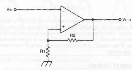
Fig. 32. Schmitt trigger which gives an output once a precise value of varying
input voltage is reached. An application of this circuit is a dc voltage level
sensor.
The twin-T feedback network is detuned slightly by adjusting the value of R4. This will usually be a miniature trimmer potentiometer. The potentiometer is set for its maximum resistance, then slowly decreased, until the circuit just begins to break into oscillation. If the resistance is set low, the sine wave will be distorted at the output.
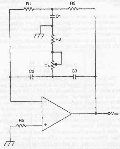
Fig. 31. A fair sine wave can be produced with this oscillator circuit.
SCHMITT TRIGGER
A Schmitt trigger is known technically as a regenerative comparator. Its main use is to convert a slowly varying input voltage into an output signal at a precise value of input voltage. In other words it acts as a voltage "trigger" with a "backlash" feature, called hysteresis.
The op-amp is a simple basis for a Schmitt trigger (see Fig. 32). The triggering or trip voltage is determined by:
V trip-
VOUT R1 R1 + R2
The hysteresis of such a circuit is twice the trip voltage.
Another Schmitt trigger circuit is shown in Fig. 33, the triggering point being approximately one-fifth of the supply voltage, i.e., there is a "triggered" output once the dc input reaches one-fifth the value of the supply voltage. The supply voltage can range from 6 to 15 volts, thus the trigger can be made to work at any thing from 1.2 to 3 volts, depending on the supply voltage used.
The actual triggering point can also be adjusted by using different values for R4, if required.
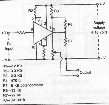
Fig. 33. A more complicated Schmitt trigger circuit for general use.
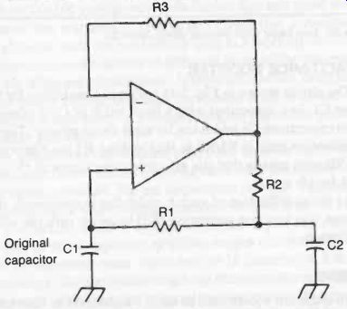
Fig. 34. Capacitance multiplier circuit. The effective capacitance Ce is
equal to the value of C1 multiplied by R-1 /R2.
Once triggered, the output will be equal to that of the supply voltage. If output is connected to a filament bulb or LED (with bal last resistor in series), the bulb (or LED) will light once the input voltage has risen to the triggering voltage and thus indicate that this specific voltage level has been reached at the input.
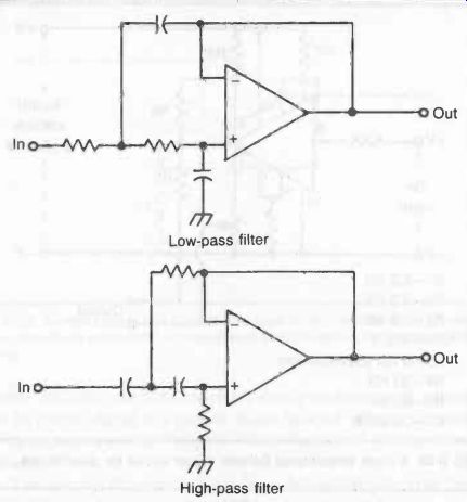
Fig. 35. Two basic filter circuits using op-amps.
CAPACITANCE BOOSTER
The circuit shown in Fig. 34 works as a multiplier for the capacitor C1, i.e., associated with a fixed value of C1 it gives an effective capacitance Ce which can be many times greater. The actual multiplication ratio is R 1/R2 so that making R1 ten times greater than R2, say, means that the effective capacitance of this circuit would be 10 x C1.
As far as utilization of such a multiplier is concerned, the circuit now also contains resistance (R2) in series with the effective capacitance.
FILTERS
Op-amps are widely used as basic components in filter circuits.
Two basic circuits are shown in Fig. 35. (See also separate section on Filters.)