Quite a number of linear ICs are designed as audio amplifiers for use in radio receivers, record players, etc. Again these are used with external components, but physical layout and the length of leads is relatively unimportant-unlike circuits carrying radio frequencies. The "packaging" of such ICs can vary from cans (usually TO-5 to TO-100 configuration) to dual-in-line and quad-in-line. In all cases they will usually have 12 or 14 leads (but sometimes less).
Not all these leads are necessarily used in a working circuit. They are there to provide access to different parts of the integrated circuit for different applications. Integrated circuits designed with higher power ratings may also incorporate a tab or tabs to be connected to a heat sink; or a copper slug on top of the package for a similar purpose.
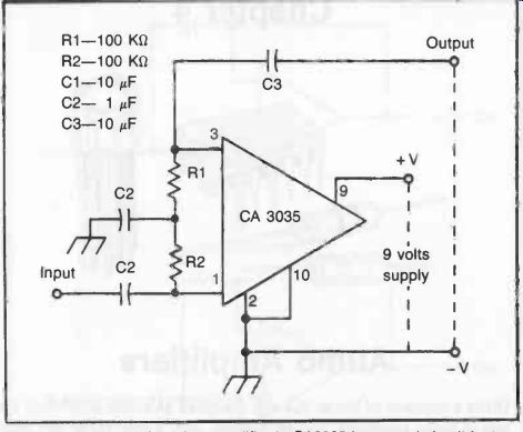
Fig. 1. Utilization of the first amplifier in CA3035 integrated circuit
by tap ping pins 1, 2, 3, 9 and 10. This circuit gives a voltage gain of 100-160
with an input resistance of 50 K-O and an output resistance of 270-Ohm.
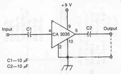
Fig. 2. Utilization of the second amplifier in CA3035 integrated circuit
by tap ping pins 2, 4, 5, 9 and 10. This circuit gives a voltage gain of 100-120
with an input resistance of 2 it and an output resistance of 170 Ohm.
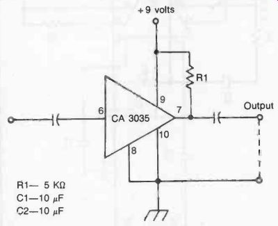
Fig. 3. Utilization of the third amplifier in CA3035 integrated circuit
by tap ping pins 6, 7, 8, 9 and 10. This circuit gives a voltage gain of 80-120
with an input resistance of 670 n and an output resistance of 5 K-ohm.
A single chip can contain one, two, three or more amplifier stages interconnected and following each other (technically referred to as being in cascade). Pin-out connections provide "tapping" points for using one or more stages separately or in cascade as required.
The (RCA) CA3035 integrated circuit is just one example. It consists of three separate amplifier stages connected in cascade with a component count equivalent to 10 transistors, 1 diode and 15 resistors. Each amplifier stage has different characteristics. The first stage, which can be selected by connections to pins 1, 2, 3, 9 and 10 (see Fig. 1), is a wide band amplifier characterized by high input resistance (i.e., ideally suited to connecting to a preceding transistor stage). The working circuit using this stage in Fig. 1. It has a gain of the order of 160 (44 dB).
The second amplifier in the CA3035 has a lower input resistance (2 K-Ohm) and a low output resistance of 170-Ohm. The gain is similar to the first stage (about 45 dB). A working circuit with tapping points is shown in Fig. 2.
The third amplifier is a wide band amplifier with a low input resistance (670 1) and a high output resistance (5 K-ohm). It offers a voltage gain of 100 (40 dB). A working circuit is shown in Fig. 3.
Amplifiers 1 and 2 can be cascaded; or amplifiers 2 and 3; or amplifiers 1, 2 and 3. Figure 4 shows the external connections and components required to cascade amplifiers 1 and 2.
Using all three amplifiers in cascade results in a gain of approximately 110 dB. The circuit in this case is shown in Fig. 5.
MODIFYING AMPLIFIER PERFORMANCE
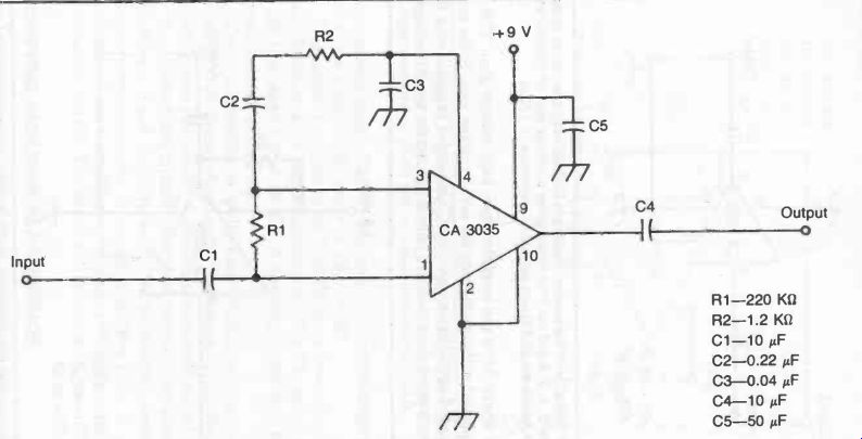
Fig. 4. Circuit for using first and second amplifiers contained in CA3035
in cascade. This circuit gives a voltage gain of about 7001 with an input of
50 ohm and an output resistance of 170 ohm.
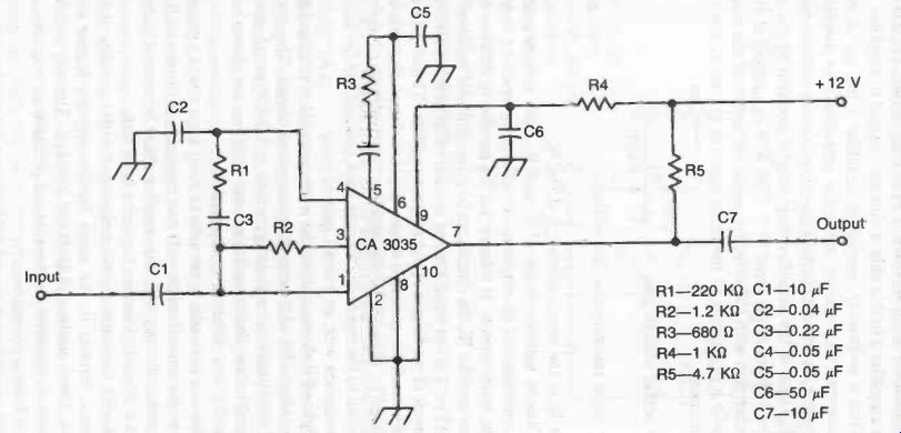
Fig. 5. This circuit shows all three amplifiers in CA3035 cascaded to give
a voltage gain of about 200,000.
The output impedance of an amplifier stage can be modified by connecting R1 to provide a negative feedback from output to input. This has the effect of reducing the working value of R1 and R1/Av where Av is the amplifier open loop voltage gain. This is accomplished without affecting the actual voltage gain. In the case of cascaded amplifiers a capacitor C2 is needed in series with R1 to act as a block to dc (i.e., R1 only is needed for amplifier 1 part [...].
Since amplifier 2 in this chip is directly coupled to amplifier 1 and amplifier 2 is directly coupled to amplifier 3 the use of an impedance-matching resistor applied to amplifier 2 (or amplifier 3) will require the use of a blocking capacitor in series with the resistor.
The gain of the amplifier stage can be modified by the use of a series resistor in the input (R1). This acts as a potential divider in conjunction with the effective input resistance of the stage so that only a proportion of the input signal is applied to the stage.
In this case: actual voltage gain = R1 / R1 + R1/Av
input resistance = R1 + R1/Av
... where R1 is the input resistance of the IC. Thus by suitable choice of R1 and Ri, both voltage gain and input resistance of an amplifier circuit can be modified to match specific requirements. It follows that if a number of different resistors are used for R1, the circuit can be given different response (sensitivity) for a given input applied to each value of R1 by switching.
This mode of working is useful for preamplifiers. Virtually the same circuit is used for an audio mixer, separate input channels being connected by separate series resistors (R1) and thence commonly connected to the input. In this case each channel has the same in put resistance with an overall gain of unity.
Figure 6 shows a circuit for a low power (1.8 watt) audio amplifier using a TA 611 monolithic integrated circuit. This particular IC is available in two configurations, a TO-100 metal case and in a quad-in-line plastic package. Lead positions are shown in Fig. 7 for the two different configurations.
This is a particularly attractive circuit for it needs a minimum number of external components and is capable of driving an 8-ohm loudspeaker directly with any supply voltage between 6 volts and 12 volts. Also, it does not require a heat sink.
Exactly the same circuit can be used with a number of other integrated circuits in the same family, offering higher output powers. These are the TA611B and TA611C. The only difference is the values required for the external components required. (See Table 1 for a comparison.)
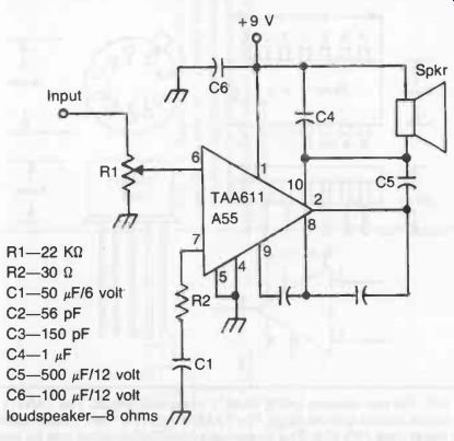
Fig. 6. Audio amplifier for radio receiver based on the TAA611 A55 integrated
circuit. Pin numbers shown are for the can-shaped version of this IC.
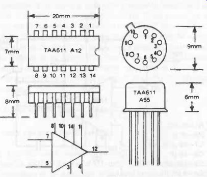
Fig. 7. The two versions of the TAA611 integrated circuit. The TAA611 A55
is a 14-pin dual-in-line package. The TAA611 A55 is a "can" shape
package in a metal case (TO-100). The circuits are identical so either can
be used in Fig. 1 with the same external components. Note, however, the different
pin-out arrangement for the TAA611 A12 on the left.
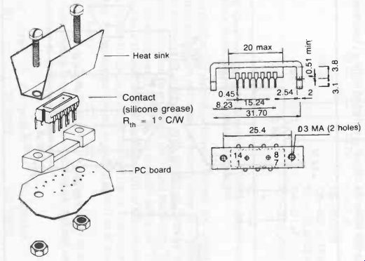
Fig. 8
Table 1. Comparison of TA611B and TA611C.
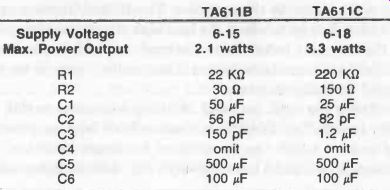
Lead arrangement for the TA611B and TA611C are the same as TAA611Al2.
Because of its higher power, the circuit based on the TA611C really requires the IC to be mounted with a heat sink although this is not absolutely essential. The IC is, in fact, available with a special mounting bar or spacer to which a heat sink can be attached.
The recommended method of mounting is shown in Fig. 8, the heat sink itself being a piece of aluminum sheet cut to a suitable size and bent to the shape shown. The IC itself has a copper slug on its top face on to which the heat sink sits (and is clamped down by the mounting bolts). Better thermal contact between the IC and the heat sink can be achieved if the contact area is very lightly coated with silicon grease.
There are other methods of fitting heat sinks to this IC (and other types). The TA611C is also available with an external bar, the ends of which can be soldered to copper "patches" on the printed circuit panel (also shown in Fig. 8). In this example the Copper areas form the actual heat sink. A suitable area in this case would be about 30 mm square for each copper patch. These copper areas are, of course, merely used for heat dissipation and are not part of the actual printed circuit as such, although it is normally advisable-and necessary with some types of IC-to connect the heat sink area to the common earth of the circuit. It is just a convenient method of making heat sinks integral with the printed circuit panel.
A further audio amplifier based on a TBA641B integrated circuit is shown in Fig. 9. This is a little more complicated in terms of the number of external components used, but has the advantage of driving a 4-12 speaker (the more readily available value with larger loudspeakers) and is suitable for direct coupling of the input. It will operate on a supply voltage ranging from 6 volts to 16 volts and give 4.5 watts output power at 14 volts. Again the IC needs mounting with a heat sink of the type illustrated in Fig. 8.
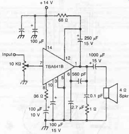
Fig. 9. Audio amplifier for 4 ohm loudspeaker based on the TBA641B integrated
circuit. Component values are shown on the diagram (SGS-Gates).
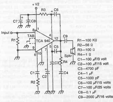
Fig. 10. 10-watt amplifier circuit based on the TCA940 integrated circuit.
The TCA940 is a 12-lead quad-in-line plastic package.
SHORT CIRCUIT PROTECTION
A feature of many audio amplifier circuits is that if the output is shorted when the circuit is switched on (e.g., loudspeaker connections accidentally shorted), excessive current may be passed by the output transistors sufficient to destroy them. It is possible to provide short-circuit protection with additional circuitry limiting the current which can flow through the output transistors. This can readily be incorporated in an IC, an example being the TCA940 designed as a 10 watt class B amplifier. Other characteristics of this particular IC are high output current (up to 3 amps) very low harmonic and crossover distortion and a thermal shut down feature (See later).
The circuit is shown in Fig. 10. Supply voltage is up to 24 volts. Power rating depends both on the supply voltage used and the resistance of the loudspeaker:
Supply voltage
4-ohm speaker
8-ohm speaker
20
10 watts
6.5 watts
18 9 watts
5 watts
16
7 watts
A feature of this circuit is that the bandwidth is controlled by the values of R2 and C3 and C7. For a value of R2 = 56 S1 with C3 = 1000 pF and C7 = 5000 pF the bandwidth is 20 kHz. For the same capacitor values the bandwidth can be reduced to 10 kHz by making R2 = 20 S1. For the original resistor value (R2 = 56 (2), the bandwidth can be reduced to 10 kHz by making C3 = 2000 pF and C7 = 10000 pF.
Circuit assembly is straightforward, except that the IC needs a heat sink. It is provided with tabs which should be bolted to an external aluminum sheet heat sink of generous area.
THERMAL SHUT DOWN
The short-circuit protection built into this IC effectively works as a power-limiting device. It is only effective on a short-duration basis, i.e., to provide protection against temporary overload and short circuiting of the output. An additional circuit is included to ensure that regardless of how long a short circuit is present across the output the junction temperature of the output transistors is kept within safe limits.
In other words, this additional piece of circuitry incorporated in the IC provides complete protection against a shorted output.
It also has another advantage. The same protection is present if there is another cause of overheating, e.g., the heat sink used is not really large enough for the job it is intended to do. The thermal shut-down circuitry simply reacts to the junction temperature becoming too high by reducing the output current and power to compensate.
HI-FI STEREO AMPLIFIER
The excellent performance and extremely good stability possible with integrated circuits makes them a logical choice for Hi Fi circuits. The TDA 2020 monolithic integrated operational amplifier is an excellent up-to-date example of such a device, designed to be used as a Class B audio power amplifier for Hi-Fi circuits.
It is capable of providing a 20-watt power output into a 4-ohm loud speaker with a supply voltage of 18 volts, and with a guaranteed output power of 15 watts. It is also a device for providing high out put current (up to 3.5 amps) and has a very low harmonic and cross over distortion. It also incorporates short-circuit protection and thermal shut-down protection.
The TDA2020 is in the form of a quad-in-line plastic package of conventional appearance with 14 leads. Because of its high power rating, it is intended to be used with a specially formed heat sink mounted on a spacer designed to provide proper thermal contact between the IC itself and the heat sink when assembled on two bolts--Fig. 11. The most negative supply voltage of the circuit is connected to the copper slug on the IC and hence also to the heat sink.
The basic amplifier circuit is completed by the addition of four external resistors and seven capacitors, plus a coupling capacitor to enable the circuit to be used with a split power supply. This provides direct drive for a 4-0 loudspeaker. Since the Hi-Fi circuits are usually stereo, two ICs are used in this basic circuit configuration, each IC powering its own loudspeaker. The complete circuit is shown in Fig. 12.
A simpler stereo audio amplifier circuit is shown in Fig. 13, based on the (Mullard) TDA1009 integrated circuit. This IC is a low frequency Class B amplifier with no crossover distortion de signed for use with a minimum number of external components.
It delivers 2 x 6 watts output power at 10 percent distortion into speakers of 4-0 impedance with 8 to 16 volts supply; and can also deliver the same power into speakers with 8-ohm impedance using a 24-volt supply. The IC incorporates short circuit protection for supply voltages up to 16 volts and also thermal protection. Input impedance is 45 K-O.
The addition of capacitors C9 and C10 (shown dotted) provides "bootstrapping." This provides increased output power.
STEREO PREAMP
In many systems, a preamplifier stage is required to bring the input signal up to a sufficient level for proper operation for the main power amplifier.
A turntable with a magnetic cartridge produces a very low level signal. A preamplifier is normally required.
In many stereo systems, the preamplifier stage also includes the volume and tone controls, and switching for selecting between the various input sources (turntable, FM receiver, tape deck, etc.).
A typical stereo preamp circuit is shown in Fig. 14. For simplicity, only the right channel is shown here. The left channel is identical. The 381A contains two independent preamplifier circuits, so a stereo (two channel) preamplifier can be constructed around a single IC. The pin numbers in parentheses are for the left channel. Pins 4 and 9 are the power supply connections, and are common to both halves of the circuit.
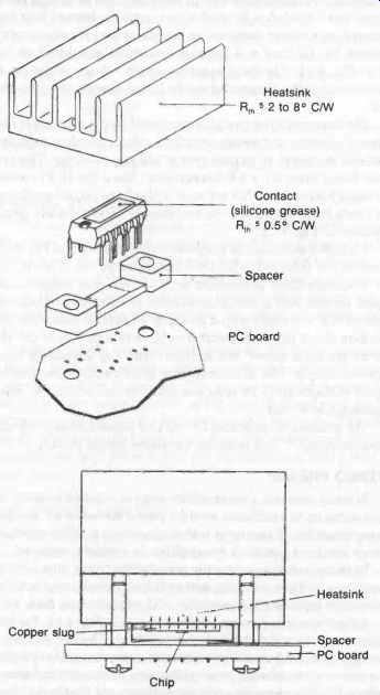
Fig. 11. Heat sink for the TDA2020 integrated circuit.
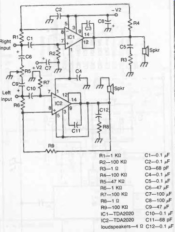
Fig. 12. Stereo amplifier circuit with split supply voltage ± 17 to ±24
volts.
This circuit features independent volume controls and source selection switching, but no tone controls. If you'd like to adapt the circuit to include tone controls, just bear in mind that a tone control is nothing more than a variable filter. Section 10 should give you plenty of information for designing tone controls.
Logarithmic taper potentiometers should be used for the volume controls.
Another stereo preamplifier for magnetic phono cartridge input is shown in Fig. 15. Both channels are shown.
This circuit is built around two sections of a 381 low noise dual preamplifier IC. In addition to independent volume controls, this circuit features independent bass and treble (tone) controls for each channel, and a balance control to set the relative levels of the two channels.
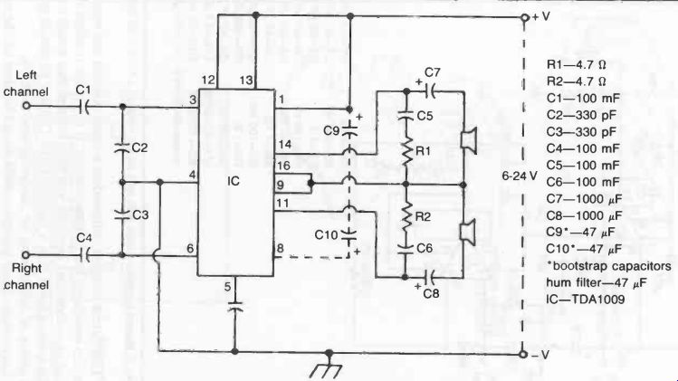
Fig. 13
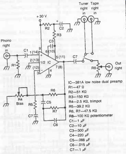
Fig. 14. Stereo preamp.
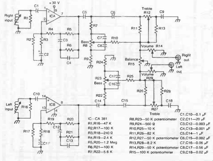
Fig. 15
HIGH POWER AMPLIFIERS
Most of the original IC audio amplifiers which appeared on the market had a relatively limited power output and thus needed to be associated with a further stage or stages of transistor amplifier-chips are now readily available with output powers from 1 to 5 watts and substantially higher outputs are obtainable from later developments capable of handling even higher voltages and currents with satisfactory thermal stability.
BRIDGE AMPLIFIERS
Even higher outputs are obtainable from bridge amplifier circuits. These can be used to increase power from output for a given supply voltage, or maintain a high power output with a reduced supply voltage. Bridge connection can give four times the output power under a given load with the same supply voltage; or twice the output power at a fixed peak current if the load impedance is doubled (e.g., using 842 loudspeaker(s) instead of 44/ loud speaker(s)).
An example of this type of circuitry, again using the TDA2020 integrated circuit is shown in Fig. 16. It is capable of delivering 30 watts power output in an 842 loudspeaker with a supply voltage of ± 17 volts.
RIAA AMPLIFIER
Theoretically, an amplifier's frequency response should be absolutely flat. That is, all frequencies should be amplified by exactly the same amount.
In some recording and transmission media, it may be necessary to pre-emphasize certain frequency components that could be attenuated excessively by the recording/transmission process.
During playback/reception these same frequency components need to be de-emphasized to restore flat response.
Standard pre-emphasis/de-emphasis curves have been devised for various media to ensure interchangeability between sources.
Virtually all phonograph records, for example, are recorded with the RIAA standard curve. An amplifier in a record player should include an RIAA de-emphasis network.
A typical circuit for a ceramic cartridge input is shown in Fig. 17.
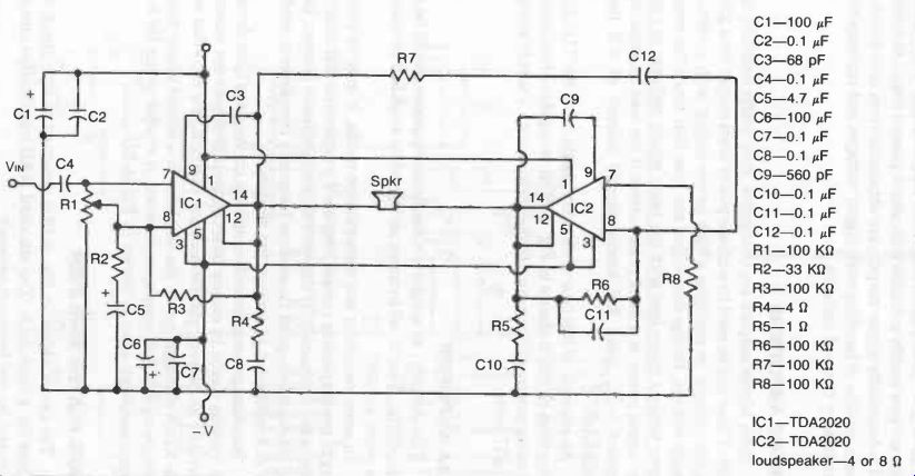
Fig. 16
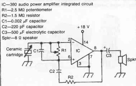
Fig. 17. Amplifier circuit compensated for RIAA.
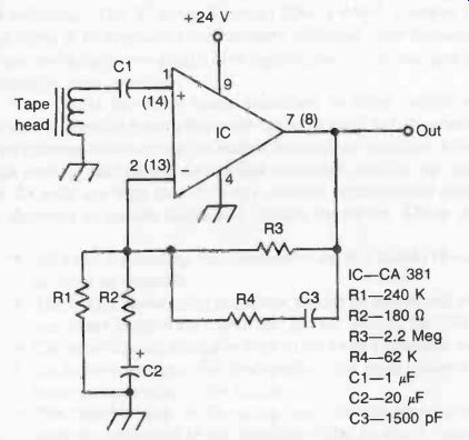
Fig. 18. Playback amplifier for a tape deck.
TAPE PLAYER AMPLIFIER
The circuit shown in Fig. 18 is designed as a playback amplifier for a tape deck. The standard NAB equalization curve is matched by the feedback network.
The tape head should be selected to generate about 800 µV at 1 kHz. The output is approximately 5 volts RMS. An external volume control potentiometer can be added to the output line.