AMAZON multi-meters discounts AMAZON oscilloscope discounts
At the heart of our development of digital design is the algorithm. It is our basic tool for organizing our thoughts, and we use it to guide the design process. The actual implementation of the control algorithm is less important than the algorithm itself. We will accept any reasonable implementation scheme that conforms to our demands for clarity, simplicity, and regularity. In Part II, we developed systematic methods of realizing algorithmic state machines using building blocks of the scale of MSI integrated circuits. Are there other ways to transform ASM charts into circuits?
From the earliest days of computers, programmers have regarded computers as machines for executing algorithms. In 1951, Maurice Wilkes* proposed building a special "computer" for executing algorithmic state machines, with the logic of the algorithm residing in a special program call1ed a microprogram. Wilkes's concept, microprogramming, was well ahead of the state of digital technology.
Microprogramming was not used commercially until 1964, when IBM employed it extensively in the construction of the System/360 series of computers.
The year 1964 also saw the beginnings of the small, inexpensive computer.
In that year the Digital Equipment Corporation introduced the PDP-8 minicomputer, which was the first CPU inexpensive enough to be dedicated to running algorithms to control a particular device. The PDP-8 and its successors and imitators enjoyed wide use for more than ten years in sophisticated digital control applications, although engineers looked upon these uses as simply an extended form of conventional programming. In 1974 another wave of technology produced the dramatically less expensive CPUs that we call microprocessors and microcomputers.
The ensuing explosion of applications will continue in the foreseeable future.
Unfortunately, many people equate the microprocessor with the concept of microprogramming, a serious misconception. Today's microprocessors and micro computers are inexpensive, small, conventional computers, programmed in a conventional way. Microprogramming represents a different approach to programming, and although many computers are constructed with the aid of micro programming techniques, the conventional software programmer normally does not use the technique. To separate these ideas more clearly, we refrain from using the sadly diluted "microcomputer" and "microprocessor" names when referring to microprogrammed devices. Instead, we will speak of a "microprogrammed controller," or "microcontroller."
CLASSICAL MICROPROGRAMMING
Wilkes recognized the fundamental separation between controller and architecture and was able to contemplate new and systematic ways of implementing the control function. Although formal ASM charts had not yet been invented, Wilkes proposed a machine whose fundamental operation was the execution of the ASM state in FIG. 1. This standard state has at most one test variable, and may have none.
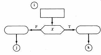
FIG. 1 The ASM state executed by Wilkes's microprogramming machine.
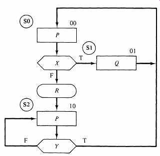
FIG. 2 An ASM with three states, to illustrate classical microprogrammed
control.
Wilkes proposed to use diodes for his machine. At that time, diodes were used to construct logic AND and OR functions. Although we no longer use diodes for this purpose, to appreciate Wilkes's proposal you should understand that diode construction provides a wired-OR capability similar to that of the modern open-collector gate.
We will describe Wilkes's method by means of an example. Consider the simple ASM in FIG. 2. Let's proceed with a clocked implementation of the state generator using an encoded state assignment of the usual sort; FIG. 2 shows an arbitrary assignment of state variables B and A for the three states.
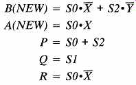
Implementing the algorithm calls for constructing the new values of the state variables, B(NEW) and A(NEW), which serve as inputs to the clocked state flip-flops. If we decode the current state variables, we may produce logic signals SO, S1, and S2 for the individual states. A routine examination of the ASM leads us to the following equations for the various outputs required in the implementation:
Wilkes proposed a systematic way of implementing these equations, which we will model as follows. Arrange the test inputs on vertical wires, with individual state signals emerging from the decoder on horizontal wires. Then, with diode AND gates, produce the branch path terms required for each state and send these horizontally to the right for use in constructing the command and next state functions. For instance, in the first step, the scheme accepts state signal SO and test input X, and produces SO·X and SO·X. Rather than use notations for diode or simple AND gates, let us suppress the detail in order to emphasize the standard, systematic structure of the design. We use a special square symbol with two outputs:
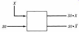
One such operation in each branching state will produce all the product terms required by the logic equations. If a state has no test input, we omit the square symbol, sending the raw state signal on to the right.
To merge the terms into final expressions, we must have a systematic way of performing the logic OR operation of the appropriate product terms. The product terms all appear on horizontal lines, so we will arrange the output signals on a second set of vertical wires, to the right of the input lines. Taking advantage of the wired OR capability of diodes, we add a diode at wire crossings where we require the OR operation. For simplicity, we show this as a dot.... The hardware will produce the OR of all the dotted horizontal signals on a vertical wire. FIG. 3 shows the implementation for the ASM of FIG. 2, using our square and dot notations for the logic operations.
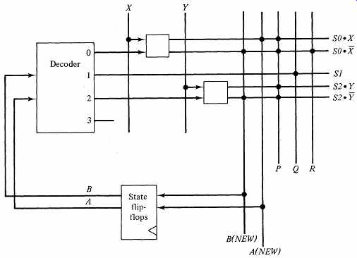
FIG. 3 A diode-based microprogrammed implementation of FIG. 2.
Wilkes's idea was masterful. Here is a systematic method of building up the random logic needed to implement any ASM with no more than one branch per state. There is another powerful way of viewing the diode matrix, which shows its close connection to conventional programming and which led to the term microprogramming. The orderly arrangement of the matrix of wires in Fig. 3 suggests a lookup table. From the discussion of ROMs in section 4 you saw that we could represent any Boolean expression as a table in which we look up the result for a particular set of values of the input variables. This was what Wilkes did, using the technology of his day; he implemented the next-state computation as a "table" of diodes. Each row at the right in FIG. 3 corresponds to a table entry for a particular branch path of the algorithm. The table entry describes the values of each output element in the system: the new values of state variables and values for each command variable. We can interpret the state machine as a primitive computer whose instruction set executes only the ASM branch operation, and whose instructions come from a special bit pattern program, a microprogram. Each row in FIG. 3 is an instruction in the microprogram; in each row, the OR dots represent I-bits, and the absence of a dot represents a 0-bit.
Why is this viewpoint powerful? We have substituted bits of memory for a random collection of gates. Since the bits of the diode array have a close correspondence to the ASM structure, and are out in the open, we may readily understand and manipulate them. Changing a Wilkes microprogram merely involves changing some diodes in a systematic manner.
CLASSICAL MICROPROGRAMMING WITH MODERN TECHNOLOGY
Let us now explore the design of microprogrammed controllers with modern devices. We will find that this causes a few changes in Wilkes's scheme, but only in the details. At the conceptual level, microprogramming remains the realization of controllers by means of tables rather than gates, an idea that survives from Wilkes. We may reduce any ASM chart to a table with inputs of current state and status variables and outputs of next-state variables and commands.
If we translate an ASM chart into a table and then implement the table directly, using hardware lookup techniques, we are microprogramming in the broadest sense. The essential step is the direct implementation of the table, bypassing gates, Boolean algebra, and so on.
To simplify our treatment, we adopt for the present a uniform representation of logic truth in the microcode. The customary convention is positive logic, with T = H; we adhere to this convention in this section. In software programming, the choice of convention is of no consequence to the programmer, who is not dealing with voltage. In microprogramming, where we remain close to the hardware, this choice of positive logic will create problems, and we will return to discuss how to reinsert the full power of mixed logic into the microcode.
If our micro controller is to implement really large algorithms, comparable to computer programs, we may need a sizable memory to hold the microinstructions for all the branch paths of the ASM. At this stage, ROM is a good choice since its contents remain intact even when the power is off. This means that the algorithm is instantly available when the power goes on, which seems quite desirable. The absence of inexpensive, fast ROM was the stumbling block in implementing microprogrammed control after its introduction, and many years of research ensued before the development of practical devices; it is no longer a problem.
In the testing of status variables newer technology has forced some changes in Wilkes's scheme. In the jargon of microprogramming, ASM variables are called qualifiers. In FIG. 3, we supply the current 2-bit state address B,A that we decode into individual signals for each state. After this decoding of the state address, we incorporate the qualifier tests using AND gates, to create one line for each decision path in the ASM. There are more branch paths than states, and each branch path results in one microinstruction. . As long as we implement the micromemory bit by bit with diodes, we can dive into the hardware following the address-decoding stage and insert or remove AND gates as needed. But ROMs and RAMs come as indivisible integrated circuits-the designer has access to address inputs and memory outputs, but to none of the interior circuitry. With RAM or ROM, the decoder of FIG. 3 is inside the device, and we have no way to get in to insert the AND gates. We need some other way to test the status variables in any given state, while preserving the table-driven nature of microcoded design.
Microprogramming with Multiple Qualifiers per State
The only way to access microinstructions stored in RAM or ROM is through the address inputs. The important elements in identifying a microinstruction are the current state and the test inputs or qualifiers. We might construct the ROM address from these two sources of bits: the current state code, obtained from the state flip-flops, and the individual qualifier signals, using one address bit for each qualifier. The size of the address field is the sum of the number of state flip-flops and the number of test inputs used in the design. For n address bits, a ROM contains 2n words. Since the ROM's size grows exponentially with the number of qualifiers, this method rapidly gets out of hand.
In this approach, the value of every qualifier contributes to each next instruction address. This is highly redundant addressing, since most of the combinations of qualifiers are of no interest. For ASMs built from such states as are shown in FIG. 1, at most one qualifier is needed in each state, yet the microinstruction address includes all the qualifiers. In general, every address is possible, so each word in the ROM must contain a valid microinstruction. Each microinstruction must supply the value of all command outputs and the value of the next ROM address:
| Next-state address | Command outputs |
Next-state Command address outputs
To illustrate this approach, let's again implement the small algorithm in FIG. 2, this time basing it on a ROM. (In practice, we would choose PROM, EPROM, or RAM, to permit more ready modification of the microcode during the development phase of the design. After the design has stabilized, we could then find a manufacturer to produce the ROMs if our production volume warranted this step. Let's use PROM in this example.) There are two state variables and two qualifiers, we must have at least 4 ROM address bits, resulting in sixteen microinstructions. We begin by exhaustively enumerating the outputs required for each of the sixteen instructions:
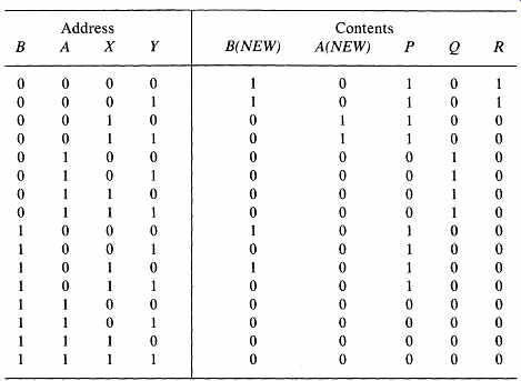
Next, we implement the table directly in a system of sixteen 5-bit words. FIG. 4 is a sketch of the circuit. All lines into the PROM are address inputs; of the 5 output bits from the PROM, 2 are inputs to the state flip-flops, and 3 are command outputs to the architecture.
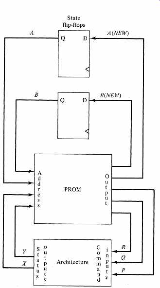
FIG. 4 A PROM-based micro programmed implementation of FIG. 2.
This approach to microprogrammed design is conceptually straightforward but requires enormous ROMs as the algorithm becomes more complex. There is an added benefit, however. Our original treatment based on Wilkes' s work allowed us to implement ASMs containing at most one test variable per state.
Since the present approach requires us to create a microinstruction for every possible combination of qualifier values for each state, we are automatically able to implement an ASM of arbitrary complexity; hence the name "multiple qualifier." No matter how complicated the branch path through a state, it corresponds to some microinstruction in this ROM-based design. Note the strong similarity to the ROM-based implementation of logic circuits discussed in section 4.
As an exercise in using the multiple qualifier method, you might wish to implement the Black Jack Dealer machine of section 6, using microprogrammed control. Suppose you use the same architecture as in the hardwired solution presented in section 6. In Fig. 6-32, you can identify two state variables (say B and A) and eight qualifiers (CARD.RDY.SYNC, CARD.RDY.DELAYED, STAND, BROKE, ACECARD, ACEllFLAG, SCOREGT16, and SCOREGT21), so the ROM address field will contain 10 bits. The number of microinstructions is 210 = 1024! The eleven command signals (including the adder select signals)
together with the two inputs to the state-variable flip-flops require that each ROM word have 13 bits. You will need a system containing a 1K x 13 ROM. You may wish to write down the contents of some of the 1024 microinstructions to solidify your grasp of the concepts in the multiple qualifier method. You can appreciate the tedium of using this "simple" method to implement a complex algorithm manually.
What is your reaction to this approach?
Ours is:
(a) It is a straightforward but tedious implementation of a general ASM. (b) The tables are very large, even for relatively small problems.
(c) The method would be feasible only with inexpensive ROMs or PROMs.
The problem is that the address for the ROM is a concatenation of a small number of encoded state-variable bits and a large number of individual qualifier bits. The state variables are important at all times in the execution of the algorithm, but each qualifier appears only occasionally in the ASM. Most of the time, the algorithm is indifferent to the value of most of the qualifiers, yet we must enumerate each combination. We are forced to use a canonical form of truth table rather than the compact form allowed by the typical ASM. This ROM-based method is feasible if you have a "smart" PROM programmer that can accept your logic equations and expand them into a canonical truth table.
But in most applications another approach might be better.
One Qualifier per State
The Wilkes scheme tests only one qualifier per state. The address is formed from the state variables alone, requiring the decoding of only a small number of variables. The scheme implements the qualifier tests with AND gates inserted in an orderly manner inside the circuit, following the decoding of the address.
You have seen that using a ROM precludes this method, and our first attempt was to move all the qualifier signals out into the address field. This allowed us to implement general ASMs, but at a severe penalty. We would like to remove the qualifier variables from the ROM address field so that we can eliminate redundant microinstructions.
Providing properly sequenced command outputs to the architecture is the purpose of an ASM. In microprogramming, the command outputs arise from bits in the microcode. In addition to these command bits, microprogramming instructions also provide the new values of the state variables. This gives us a clue: our microcode has two components, an external one (command outputs)
and an internal one (the next microinstruction address). Perhaps by enlarging the internal portion of the microinstruction we can shrink the number of instructions.
We are striving to develop a method of handling large problems, and we may have to compromise the generality of the ASM structures that our method will handle.
Let's start instead with the most elementary useful ASM operation; one qualifier per state with no conditional outputs. Further, let's try to realize each state with only one microinstruction. In such a scheme, the ROM address would consist solely of the state variables, which would select the proper microinstruction.
This instruction must contain sufficient information to guide the development of the next-state address. In particular, the instruction itself must specify which qualifier this particular state is testing.
If we organize all the qualifiers in a list, we may designate any qualifier by its index n in the list. The ASM structure we are trying to realize is
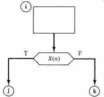
where X(n) is one of the qualifiers X. Let's include this index n-the qualifier index-in the microinstruction. Then, in our single microinstruction for state i, we must also include the next-state addresses j and k for the true and false branches. Each microinstruction in our ROM will now look like:
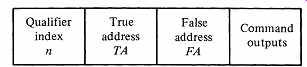
Each word is now wider than in the multiple qualifier method, since it includes the index field and an extra address field, but our microinstruction table is reduced to one row per state.
To execute a microinstruction, our primitive microcontroller must be able to select the proper X(n) using the value of n in the instruction. Based on the present value of the selected test input X(n) the processor must choose one of the two address fields as input to the state flip-flops. Let's construct this selection hardware. Index n is an address in a table, so we may use a multiplexer building block with n as the code for the test input selection. The output of this multiplexer is a variable X(n), whose value must specify either the true or the false address.
We can perform this last selection with a set of two-input multiplexers, using X(n) as the select input. FIG. 5 is the circuit for our processor.
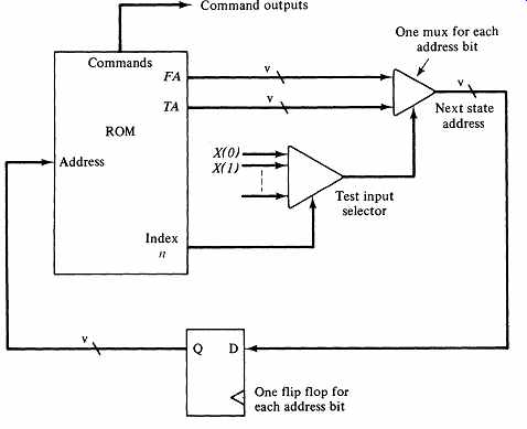
FIG. 5 A primitive microprogram controller with an input qualifier index
and both true and false jump addresses.
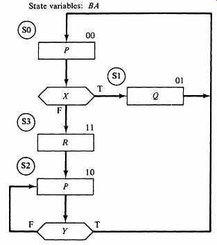
FIG. 6 FIG. 2 redesigned to have no conditional outputs.
To illustrate the use of this microprogrammable machine to execute an algorithm, we will write the microcode for the ASM of FIG. 6, which is a variant of FIG. 2 modified to eliminate the conditional output. Assigning indices 0 and 1 to the qualifiers X and Y, respectively, yields the following four microinstructions:
TA and FA each require 2 bits, n has 1 bit, and there are three command outputs, so this design would require four words of 8-bit ROM.
Unconditional state transitions occur in instructions 1 and 3. Since each microinstruction must specify the index n of some test variable, we simply choose any index and make both TA and FA point to the same next instruction.
Why did we eliminate the ASM's conditional output from our single-qualifier scheme? Conditional outputs arose naturally in Wilkes's scheme and in the multiple-qualifier approach. But here we have exactly one microinstruction per ASM state, and all the information for the execution of that state must reside in that microinstruction. If we were to permit conditional outputs, we would need a way to designate, for each command output bit, whether it is to be asserted unconditionally, or only on the true branch, or on the false branch, or not at all. This would require 2 microinstruction bits per command output-a considerable burden on the hardware. One of the virtues of the present method is its simplicity of form. Another reason for eliminating conditional outputs will surface later.
Single-Qualifier, Single-Address Microcode
The preceding single-qualifier structure is feasible, but the two address fields can consume considerable space in the microinstruction. We can eliminate one address field if we adopt a rule for inferring that address from the present address.
The obvious choice, which conforms closely to the practice used in conventional computers, is to insist that one of the branch addresses be the next sequential address. In the single-qualifier method, state assignments correspond to micro instruction addresses, and since the state assignments are at our disposal, we may use normal sequencing to save bits in the microinstruction. The ASM operation reflecting this modification of the single-qualifier scheme is shown in Fig. 10-7a.
The microinstruction now contains one jump address, the qualifier index, and the command output bits. In the version of ASM in FIG. 7a the jump address is always the true path. We can enhance the versatility of this approach by adding one more bit to the microinstruction, to allow the microprogrammer to specify which path, true or false, the jump address refers to. Now the format for the microinstruction is
This form of microprogramming implements the basic ASM operation in Fig. 7b.
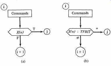
FIG. 7 ASMs for single-qualifier, single-jump address microinstructions. (a)
Microinstruction branches on a true qualifier. (b) Microinstruction allows
selection of the jump condition.
Now consider how we might build the processor for this method. Since we have eliminated one of the address fields, we have also removed the need for the two-input multiplexers on the state flip-flop inputs in FIG. 5. Instead, we need to be able to increment the current address whenever the test variable value is opposite of TFBIT in the microinstruction. We may incorporate this operation into our state flip-flop assembly by replacing the simple flip-flops with a programmable binary counter building block. Our micro controller processes a microinstruction in each clock cycle, so we are always either branching, which corresponds to landing a new value into the counter, or sequencing the counter.
With the aid of the ASM in Fig. 7b, we may derive the condition for loading the counter. We load the counter whenever the next address is to be the microinstruction jump address fA:
(NEXT.ADDRESS = fA) = X(n)oTFBIT + X(n) oTFBIT
= X(n) 0 TFBIT
We sequence the counter whenever we do not jump. An implementation of this microprogrammable controller is shown in FIG. 8.
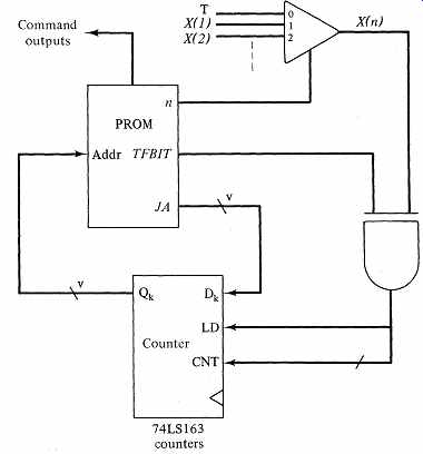
FIG. 8 A counter-based implementation of the microinstruction control
in Fig. 7b.
Another convenience shown in FIG. 8 is making test input position 0 a permanent true signal. The microprogrammer may then execute an unconditional branch (no test variable) by designating n = 0 and TFBIT = 1 in the microinstruction. Conversely, unconditional sequencing to the next instruction· occurs when n = 0 and TFBIT = 0.
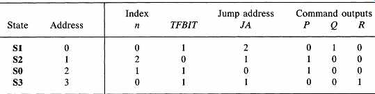
Having constructed this sophisticated single-qualifier controller, let's use it for the simple ASM in FIG. 6. Earlier, when we used the single-qualifier method with two address fields for this algorithm, our exact choice of state assignment was unimportant. (Why?) In the present method, we are required to make one of the exits from each state sequential. We encounter difficulty with the assignment in FIG. 6 since, as it happens, neither branch from state S2 is sequential. T() avoid this problem, we may renumber the states in FIG. 6 so that S0 = 2, S1 = 0, S2 = 1, and S3 = 3. If we assign indices 1 and 2 to qualifiers X and Y, respectively, the microcode for the program is
As another illustration, we could implement the Black Jack Dealer of section 6 using the sophisticated single-qualifier scheme. The ASM is not suitable, since it contains conditional outputs and states with multiple tests.
Converting this ASM to an appropriate form is a useful exercise. In most cases, we may convert a conditional output to an unconditional one by creating a new state for the output. This simple method will not work when the exact timing of ' the conditional output is crucial; an example is in the GET state. If we create a separate state for the HIT output, the hit light will blink on and off as the ASM loops around the two-state loop. We will deal with this particular problem presently.
States with multiple tests also require modification before we can use the single-qualifier method. Where the timings are not critical, we may create new states to perform each individual test. This approach would handle all cases except the first two tests in the GET state. You will recall that this structure is a manifestation of the familiar single pulser; it requires that CARD.RDY.SYNC and CARD.RDY.DELAYED be tested simultaneously. For the Black Jack Dealer algorithm, the solution, which also solves the problem of the HIT output, is to use one of the other forms for describing the action of the single pulser. (Notice how valuable was the knowledge that this troublesome structure represented a standard design element. How much more difficult the analysis would have been without this knowledge!) FIG. 9, the result of the ASM transformation, is a version of the Black Jack Dealer algorithm that we may implement as a single-qualifier microprogram.
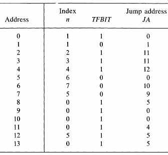
FIG. 9 contains an address (state) assignment that makes good use of the requirement that one branch of each state must lead to the next sequential state.
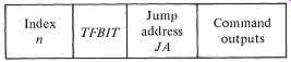
We have made an arbitrary choice of the qualifier index, and have shown the index in brackets in each test in the ASM. Here is the microcode for the Black Jack Dealer of FIG. 9, without the command outputs. You should find it easy to include command bits in each microinstruction. What is the size of the ROM required by this microprogram?
Comparison of the Microprogramming Approaches
We have considered microprogramming from two viewpoints. How does the single-qualifier approach compare with the multiple-qualifier method? Some facts to consider are: (a) The single-qualifier method has a one-to-one correspondence with an ASM chart; the multiple-qualifier method does not.
(b) The single-qualifier method requires much less microcode.
(c) The single-qualifier method will handle large problems easily; the multiple qualifier method cannot tolerate many qualifiers before it becomes unmanageable.
(d) The multiple-qualifier method handles a completely general ASM; the single qualifier method handles only a special case.
(e) The single-qualifier method requires more special hardware in the micro controller, although the multiple-qualifier method requires the larger ROM.
From these points we may draw some conclusions. The single-qualifier method is clearer and easier to manage. It is more likely to result in correct microcode the first time. Field-service personnel are more likely to understand single-qualifier programs and they are much easier to document.
Item (c) is probably decisive, but even so, our sense of style leads us to recommend the single-qualifier method for most applications.
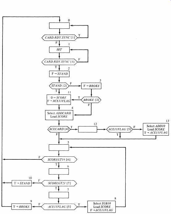
FIG. 9 The Black Jack Dealer ASM revised for microprogrammed implementation.
MOVING TOWARD PROGRAMMING
As we have developed the concepts of microprogramming in this section, our language and our emphasis have come ever closer to those of the software programmer. We began by emphasizing hardware, looking for ways to systematize the design process to handle large problems. We followed Wilkes through his discovery of table-driven hardware controllers. We finally arrived at a design of a machine that executes only a restricted form of ASM operation but that executes all such operations in a systematic manner. We call the specification of each standard ASM state a "microinstruction," and we refer to the state variable values as a "memory address." We think in terms of writing a set of instructions-a microprogram-to describe an algorithm for this specialized machine, and we place the program into a memory.
It sounds like programming, but how far have we gone? Microprogramming is a middle ground between hardwired design and conventional programming, drawing advantages from each. From the viewpoint of the designer of hardware, microprogramming offers a way to tackle large and complex control problems.
It retains much but not all of the speed and capability of parallel action that is characteristic of hardwired ASM implementations. The single-qualifier approach to microprogramming permits the designer simultaneously to receive status in formation, control the flow of the algorithm, and issue detailed commands to the controlled device. We lose multiple branches and conditional outputs and also a bit of speed, but we gain a compact, highly structured, easily modified method of formulating and implementing algorithms. At the other end of the microprogramming spectrum, the multiple-qualifier approach costs nothing in speed or in the flexibility of the algorithm, but tends to overpower the designer with its exponentially increasing size of microcode.
The software programmer sees microprogramming as an entry into the field of hardware. The serial, one-step-at-a-time nature of conventional programming gives way to a more parallel but still program-oriented approach. The micro controller has a more primitive command structure than a conventional computer, yet the simple but parallel nature of its operations makes for much greater speed and versatility.
Why do we stress the programming aspect? Why has microprogramming come to be considered a conceptual breakthrough in hardware design? The answers lie in the great store of experience that computer science has gained in using programs to emulate algorithms. Conventional programmers have a host of software tools and strategies that we can use in microprogramming. By transforming a hardware problem into the programming domain, we may look forward to using editors, assemblers, language translators, and debugging aids in support of the development of our microcode.
Let us try, then, to borrow from programming concepts to expand the usefulness of microprogrammable controllers, without detracting from their inherent power as emulators of hardware algorithms.
Cleaning Up the Outputs
Throughout our development of microprogramming, the microinstruction memory ROM, PROM, or RAM-has been the source of command outputs to the architecture and control signals to the next-state controller. Unfortunately, these memories undergo relatively long periods of instability when their address inputs change, and so the signals emerging from the memory outputs have undesirable voltage characteristics. Our circuits for sequencing microinstructions have worked despite this drawback, since the changes in the memory addresses have been synchronized with the system clock. The architecture is exposed to the impurities of the command outputs, but since it is driven by the same clock as the control unit, the designer may use these outputs reliably to feed the clocked architectural elements. The command outputs are unsatisfactory for non-clocked uses, such as serving as control signals to the world outside the clocked design. In these important cases, the designer must purify the command outputs, usually by passing them through a clocked flip-flop to assure a clean output.
The microinstruction memory has served as an instruction register, but in recent practice the role of instruction register is removed from the microprogram memory and is assumed by a true clocked register. This register, known as the microinstruction register or pipeline register, receives the full output of the microinstruction memory and delivers clean, reliable signals to the architecture and to the circuits that produce the next microinstruction address. The designer then has a uniform and reliable interface with the microprogram control unit.
Enhancing the Control Unit
Just as FIG. 8 grew out of consideration of more primitive controllers, we may generalize it to produce a more powerful controller. In FIG. 8, the counter and the coincidence gate perform a control function that responds to inputs and produces an output. The inputs are the test input signal from the external architecture and the TFBIT and jump address from the present microinstruction.
The output is the address of the next microinstruction. We may view the TFBIT and jump address as components of an elementary computer branch instruction, and the counter and coincidence gate as a primitive computer control unit. In this view, FIG. 8 implements a computer with one flow-of-control instruction, a simple branch. But ordinary computers have much more sophisticated branching than this, so why should we not incorporate some of this sophistication into the next-instruction-address evaluator within our microinstruction control unit? We will view a microinstruction as consisting of two components, a microinstruction sequencing part and a command output part:
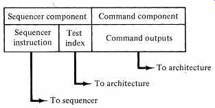
The sequencing component of the microinstruction becomes an instruction to be processed by a microprogram sequencer, contained within the microprogram control unit. The sequencer and its instruction input may be relatively simple, as in FIG. 8 and earlier figures, or it may be quite sophisticated. Our view of the microinstruction control unit has been transformed into FIG. 10. With these moves, we have a structure that is close indeed to conventional computers, yet retains much of the power of hardware. Our microprogram control unit has a memory, an instruction register, and is capable of determining the microprogram's flow based on the present state of the system and an external input.
With these expanded capabilities, we can express quite complex control algorithms. Our new model of a microprogrammable controller (FIG. 10) still implements an ASM similar to FIG. 7 in which all command outputs are unconditional and control of the microprogram either moves to the next sequential state or branches to a new state in response to the test of a single input signal.
However, the possibilities for branching are considerably enlarged. We will see that we may use subprogram calls and returns, loops, and other useful constructs from the programming world. The opportunity to express highly complex algorithms as microprograms means that the designer will need sophisticated aids to support the development, debugging, and maintenance of the microprogram. At the same time, the architectures to be managed by these more complex algorithms become larger and more complex, requiring additional aids for hardware development.
Several microprogram sequencers are available as integrated circuit chips.
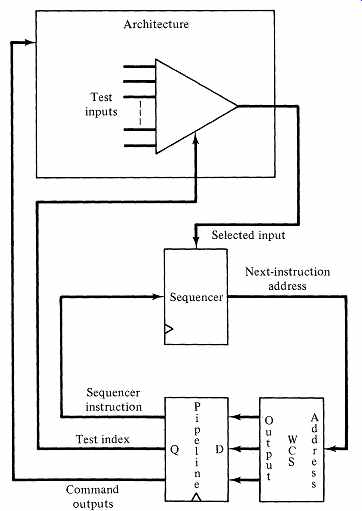
FIG. 10 A sophisticated micro program sequencer.
The first was the 2909, introduced by Advanced Micro Devices in 1975. The 2909 accepts a 2-bit operation code and provides 4 bits of next-instruction address; several 2909s can be cascaded to produce larger addresses. The 2909 supports conditional branches and subprogram calls and returns. As the technology advanced, more address bits were provided within a single chip and more complex operations were introduced. For instance, the 2910 integrated circuit produces 12 bits of next-instruction address and executes 32 instructions. The Texas Instruments 74AS890 supports 64 instructions and has 14 address bits.
The 2910 Microprogram Sequencer
Microprogram sequencers are sophisticated devices with many features . We will limit our discussion to the 2910 and those characteristics that support our study pf microprogramming. If another micro sequencer is used, it will have similar characteristics. FIG. 11 shows the principal signals entering and leaving the 2910. The 2910 is designed to produce the address of the next microinstruction to be loaded into the pipeline register. It accepts a 4-bit operation code I, a test-input signal CC (Condition Code), a control signal CCEN (Condition Code Enable) to guide the use of the test-input signal, and a 12-bit data-Input field D. The D-field usually provides a microprogram branch address (our familiar jump address) from the pipeline register, although it has other uses in the 2910. The output of the 2910 is a 12-bit next-instruction address Y. The 2910 can support microprograms containing up to 4096 instructions. Since the 2910 contains internal registers, we must supply a system clock signal CPo FIG. 12 shows the internal architecture· of the 2910. The next-instruction address Y originates from one of four sources, selected by a 4-input multiplexer based on the operation code and the value of the test input signal. Two of the four sources are already familiar to us: the next sequential address (current microinstruction address + 1), and a branch address derived from the current microinstruction. The 2910 contains a microprogram counter-register ({JPC) which records Y + 1, the next sequential address, in case it is needed later.
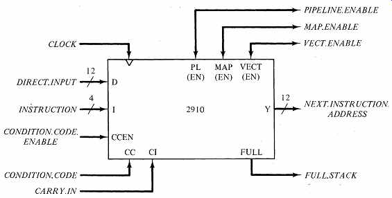
FIG. 11 The 2910 microprogram sequencer.
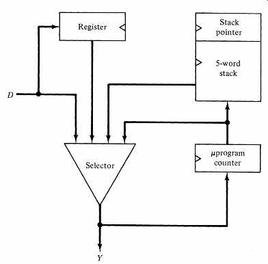
FIG. 12 Twelve-bit data paths in the 2910 microprogram sequencer.
The output of the p,PC forms one input to the Y multiplexer. The 12-bit external data input D forms another multiplexer input. Usually ,.D comes from the jump address field of the pipeline register.
The two remaining multiplexer inputs support subprogram calls and program looping. The 2910 contains a five-word stack. In a subprogram call, the 2910 must save the return address on the top of the stack; a subprogram return must supply the return address from the top of the stack. The 2910's internal stack allows calls to microprogram subprograms to be nested five deep. Each subprogram call results in a stack push operation, and each subprogram return causes a stack pop operation. When a microinstruction executes a subprogram call, the required return point is the address of the control store word following the subprogram call instruction. This address is exactly the quantity that is currently stored in the 2910's p, PC; FIG. 12 shows a data path from the p,PC to the stack that supports subprogram calls.
The fourth input to the Y multiplexer is from an internal register R that can hold a loop counter. The R-register can be loaded from the 2910's D-input.
Several 2910 instructions support the loading, testing, and decrementing of the value in the R-register.
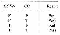
The 2910's 4-bit operation code supports 16 basic instructions. Each instruction has a "pass" and a "fail" option, generating a total of 32 possible operations. The selection of pass or fail is controlled by the values of the 2910 inputs CC and CCEN, according to the following prescription: if the enable signal CCEN is true and the test input (condition code) CC is false, then fail; otherwise pass. Viewed another way, this structure allows the execution of the pass version of an instruction when we are not testing the input, or when the input is true while we are testing it. The following table specifies the conditions for selecting the option:
CJP (conditional jump) is a typical 2910 instruction. In its fail mode, this instruction selects the μPC as the Y-output, accomplishing normal sequencing.
In its pass mode, CJP selects the D-input as the Y-output, thus performing a branch. At the next system clock edge, the pipeline register will receive the appropriate instruction and the 2910's μPC will capture the address + 1 of this instruction.
Another example is CJS (conditional jump to subprogram). In its fail mode, CJS sequences to the next microinstruction address, with no effect on the 2910's internal stack. In its pass mode, CJS performs a subprogram jump, which selects the branch address in the D-input as the value of Y, and, when the system clock fires, causes the contents of μPC to be pushed onto the internal stack. (As usual, μPC will receive the new Y + 1 when the clock transition occurs.) In the fail mode, the instruction CRTN (conditional subprogram return) performs normal sequencing, with no effect on the 2910's stack. In the pass mode, CRTN delivers the top-of-stack element to Y, thereby supplying the return address to the previous subprogram as the address of the next microinstruction.
When the clock transition occurs, the 2910 pops its stack, and μPC receives Y + 1.
When the 2910 is used as the sequencing element in FIG. 12, an appropriate form for the flow-of-control portion of the microinstruction is:
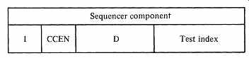
Each microinstruction provides the 2910 with the I, CCEN, and D fields. The index field goes to the architecture to guide the selection of the appropriate test input, which becomes the 2910's CC input.
Thus far, the 2910's D-field arises from the corresponding field in the microinstruction pipeline register. Although this is by far the most common and useful mode of operation, the 2910 also permits an alternative source of the D input. With each instruction, the 2910 asserts one of three D-field selection signals. In the instructions described above, the 2910 asserts its Pipeline-Enable signal PL(EN). On the other hand, the 2910's JMAP (Jump on Map Address) instruction, which causes an unconditional jump to the D-field address, asserts the Map-Enable signal MAP(EN) instead of PL(EN). This feature provides a limited yet useful capability to select the D-field input from a source in the designer's architecture, under control of the MAP(EN) signal. We will use this feature of the 2910 in a subsequent design example. One other 2910 instruction has similar characteristics; all other instructions cause the assertion of PL(EN). If MAP(EN) is chosen, all inputs to the 2910's D-field must have three state characteristics and the designer must use the 2910 PL(EN) and MAP(EN) signals to select the proper input.
TABLE 1 is a summary of the 2910's instructions. In this section we use about half of these instructions, and will explain each new instruction at the time of use. Consult an AM2910 data sheet for additional information, if you desire. The instructions CJP, CJS, CRTN, and CONT (Continue) are by far the most commonly used 2910 instructions. In this section, we use the alternative mnemonics JUMP, CALL, and RTN in place of CJP, CJS, and CRTN. Choosing a Microprogram Memory With the realization that our microprogramming methods are capable of describing and executing quite complex algorithms, we begin to see the need for sophisticated equipment to help the designer to manage the complexity. We have assumed that the microprogram storage was a read-only memory-ROM, PROM, or EPROM. In accordance with good programming practice, our microprograms do not change; all the "data storage" is in the architecture. Even when sophisticated microprogram sequencers such as the 2910 are used, the microprogram remains fixed during execution-the sequencer itself contains storage for sub program return points and loop control. For such an environment, ROM seems the natural choice. Many designers initially discarded RAM for this purpose because of the volatility of its contents when power drops. But as the size and complexity of modern microprograms have increased, this choice has been reversed.
For debugging complex microprograms, and when the microcode may be modified in the field, RAM is essential. In microprogramming jargon, the microprogram storage is the control store. If the control store is easily alterable, as is RAM, it is called writable control store (WCS). If we use RAM, we must load it frequently, and we need powerful microprogramming aids. In the next section we describe a microprogrammable development system that provides the designer with the hardware and software tools required to manage the design and development process.
THE LOGIC ENGINE--A DEVELOPMENT SYSTEM FOR MICROPROGRAMMING
Microprogramming permits the designer to tackle complex control tasks, but this ability to deal conceptually with complex designs entails numerous practical problems. On what type of breadboard should we construct the architecture? How do we debug the architecture? How do we produce the microcode? How do we load the microcode into a control store? How do we design and build the microinstruction sequencer? How do we debug the microcode? How do we modify the microcode? These questions imply that designers need a powerful support system to allow them to manage microprogrammed control. The control unit is itself only one part of a good development system. The system must also support the development and debugging of the architecture and the control algorithm. It should minimize the usual headaches of design and the subtleties of constructing the hardware. It should provide for convenient wire-wrapping for initial testing, and for lights and switches for displaying and controlling individual signals during the testing of the design, as well as lend powerful support to the development, debugging, and modification of the control program.
Several commercial microprogrammable development systems have appeared.
We will describe one of these, the Logic Engine, which we designed and built.
Our goal is to reach a position from which we may easily produce and manage complex hardware projects using microprogrammed control. The goal is ambitious, and to achieve it requires an understanding of the design principles and practices presented in this section.

TABLE 1 INSTRUCTIONS OF THE 2910 MICROPROGRAM SEQUENCER
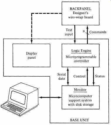
FIG. 13 The Logic Engine.
FIG. 13 shows the parts of the Logic Engine Development System.
The base unit houses the microprogrammable controller, a microcomputer-based debugging support system, and a debugging display panel. Attached to the base unit is a large, detachable back panel for wire-wrap of the hardware architecture.
A terminal provides for convenient interaction between the development system and its user.
The Base Unit
The Logic Engine's microprogrammable control unit contains a 2910 microprogram sequencer, a writable control store of up to 4K words, a microinstruction pipeline register to deliver command signals to the designer's architecture, and a buffer register to support communication between the controller and the microcomputer based monitor. FIG. 14 shows the structure of the Logic Engine's controller.
The task of the controller is to present a properly sequenced set of signal voltages (commands) to the designer's architecture. Therefore, a Logic Engine micro instruction has two primary fields: a fixed-format sequencing field to direct the 2910 in the production of the address of the next microinstruction and an open ended field for specifying command signals to the designer's circuit. The sequencing field consists primarily of the items required to direct the 2910: I, CCEN, and D. The length of the command-bit field is determined by the particular project and may exceed 100 bits.
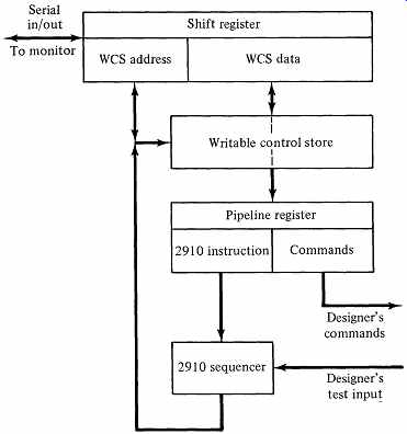
FIG. 14 The architecture of the Logic Engine controller.
The designer may choose two ways of executing the microinstructions. In the automatic mode, the controller loads microinstructions from the writable control store (WeS) into the pipeline register under the control of the 2910 sequencer. In the debugging mode, the designer can influence the delivery of command signals to the architecture in several ways, using features of the Logic Engine's debugging monitor.
The Logic Engine's support system consists of software running on a microcomputer inside the base unit. The microcomputer has dual floppy-disk drives, two serial input-output ports, and one parallel input-output port. The parallel port provides the interface between the support system and the Logic Engine's controller. One serial port is dedicated to the designer's display terminal; the other serial port is available for connecting a serial printer, remote computer, or other device. The Logic Engine's support software is organized around a debugging monitor. Additional software includes a text editor, a microprogram assembler, and various utility programs.
The Logic Engine's display panel provides about 100 LEDs for displaying data, over two dozen pushbuttons and toggle switches for entering data, and a variable-speed clock that includes a manual mode. The designer has access to these whenever the back panel is attached to the base unit. The base unit contains a power supply adequate to operate the Logic Engine and the designer's circuit.
The Back Panel
The Logic Engine's back panel is large: 16 in. wide and 20 in. high. It has a general-purpose work area to handle integrated circuit chips of 8 to 64 pins. For a typical design, the back panel can accommodate several hundred chips. The designer has access to both sides of the board at all times. Ground and +5 V appear as power grids on opposite sides of the board and there are extensive provisions for attaching power-bypass capacitors (see section 12). Along one side of the back panel is an area committed to the microinstruction pipeline register and WCS for the designer's command signals. This permits easy wire-wrapping of the command signals to the architecture, and allows the designer to employ as many command signals as the design requires.
The Supporting Software
The Logic Engine's development and debugging monitor supports the detailed control of the WCS and of the operations of the microprogram sequencer and pipeline register. The designer may load the WCS from a floppy-disk file-an example of downloading. The designer may read and modify any word in the WCS, modify any word without disturbing the remainder, and display the contents of a block of WCS. Since the 2910 microprogram sequencer is an integral part of the Logic Engine, the monitor knows its characteristics in detail and thus can support the display and modification of all of the sequencer's internal registers.
The designer may display the microinstruction pipeline register and modify any portion of it. The monitor also permits the designer to specify whether, with each manual change of the pipeline register, a designer's clock signal is to be issued. These features give the designer an important debugging tool: the manual entry of microinstructions into the pipeline register without modifying the writable control store. Since the pipeline register's command field is wired to the designer's architecture, the designer may exert detailed manual control of the circuit.
TABLE 2 summarizes some of the functions of the Logic Engine's monitor that are available to the designer. In executing microcode from the WCS, the most powerful debugging features are single-step and breakpoint. Single-step permits the designer to execute one instruction at a time from the WCS, with a complete Logic Engine register dump accompanying each instruction. The breakpoint feature is used when the designer is running microcode at high speed.
The designer announces a particular WCS address that, if it becomes the candidate for next microinstruction, will cause the controller to halt. Breakpoints permit the designer to stop the execution of instructions at any address and then observe the status of the system.
TABLE 2 FUNCTIONS OF THE LOGIC ENGINE'S MONITOR
M Display and modify the WCS
E Examine a block of the WCS
R Display and modify the Logic Engine's registers
P Load the pipeline and execute an instruction
C Clear the 2910
B Set or clear a breakpoint
G Go! (Run microcode from the WCS)
I Idle the Logic Engine
S Execute a single instruction
H Help!
L Load the WCS from a disk file
U Unload the WCS to a disk file
The Logic Engine's microprogram assembler provides powerful development features within a structured microprogramming language. The microassembly language encourages the designer to express the control algorithm in high-level terms and provides for transforming the high-level specification into microcode.
The assembler supports the symbolic naming of single command bits and fields of bits, and there is a convenient syntax for invoking the desired values of the command bits. The assembler provides full mixed-logic capabilities, giving the designer the freedom to specify signal values as voltages or as logic levels and to describe the voltage convention for truth for each signal. The designer may specify default values for command signals, so that in writing microcode only command signals that deviate from the default values need be described. In the sequencing portion of the microinstruction, the assembler supports the 2910's instruction set and has a convenient syntax for specifying the designer's test inputs.
NEXT>>
Related Articles -- Top of Page -- Home