AMAZON multi-meters discounts AMAZON oscilloscope discounts
DESIGNING AND DEBUGGING WITH THE LOGIC ENGINE
To illustrate the process of design using microprogrammed control, let's study the design of a small portion of a machine that can directly execute the Forth language in hardware. (It is not necessary to know the Forth language to follow the example.)
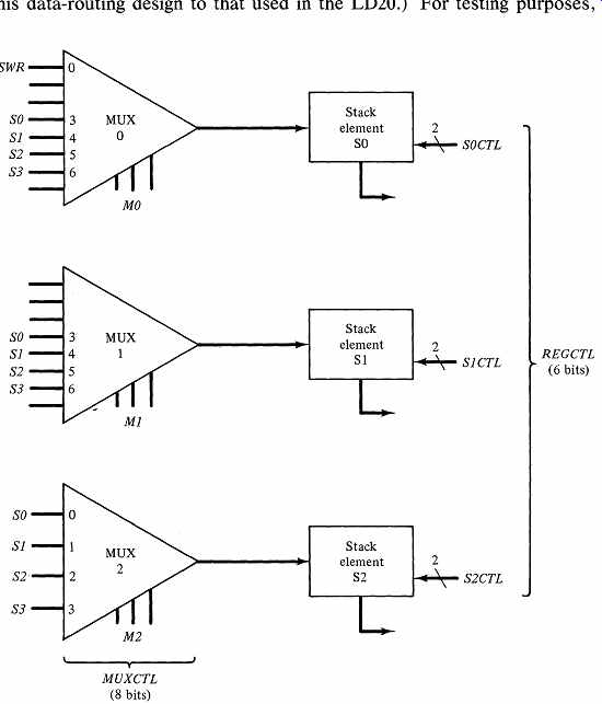
FIG. 15 The architecture of a microprogrammed design.
The Initial Design
Our first step is to work out the architecture-the registers, busses, and data paths. Forth is a stack-oriented language, and several of its important operations involve manipulations of the elements on the stack. In this example, we focus on the stack operations. We wish the several top elements of the stack to be available for direct use; the deeper elements will be kept in a RAM. FIG. 15 is a portion of the architecture, showing the top three elements of the stack.
(The stack elements may contain as many bits as required by the problem, but this decision does not concern us here.) The input to each stack element is through a set of multiplexers. Each of the potential sources of a given element of the stack becomes an input to that element's multiplexer. (Notice the similarity of this data-routing design to that used in the LD20.) For testing purposes, in addition to the elements of the stack, inputs include the switch register on the display panel. We will call the select signals for the three multiplexers MO, M], and M2, and refer to the entire collection of multiplexer select signals as MUXCTL. In addition to holding its contents and loading new information, each element of the stack may perform internal bit-shifting operations. To support these activities, each stack element requires 2 control inputs; for stack elements, SO, S], and S2, we call the stack controls SOCTL, S] CTL, and S2CTL, and we call the collection of six stack-element controls REGCTL. The next step in the design is to work out, in rough form, the algorithms to control the architecture. The thought put into this step will often lead to modifications of the architecture. The design process involves moving between increasingly refined sketches of the architecture and control until we feel reasonably confident that we understand our problem thoroughly. Then there is hope that when we build our machine, it might actually work! At this stage in the design of the algorithm, we can see what signals from the architecture we must test in our microcode in order to direct the flow of the microinstructions. The 2910 sequencer accepts a single signal as a test input, and the 2910's instructions may act upon the value of this signal. Consistent with our earlier development of microprogrammed controllers, we place a test input multiplexer in the Forth Machine's architecture to deliver the single test signal to the 2910. Since we know which, if any, signal is required for testing in each microinstruction, we may use some of the microinstruction's command bits as the select code for the multiplexer. The full Forth Machine design requires about a dozen test inputs, so a 16-input multiplexer with a 4-bit select code is appropriate. FIG. 16 shows the structure of the apparatus for selecting test inputs, including the two that we use in this design. We have allocated the first 4 microinstruction command bits (bits 0-3) to the control of the test multiplexer; this is an arbitrary choice.
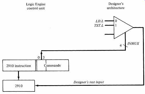
FIG. 16 Structure of the test input in a microprogrammed design.
The Initial Testing of the Architecture
Now it is time to construct and test the architecture. On the Logic Engine's back panel, we layout the chips required by the architecture, assemble the appropriate sockets and chips, and wire-wrap the design. The size of the back panel permits us to develop and debug the architecture without partitioning the components among small printed circuit boards.
At this point, we usually make some preliminary tests of the registers and the data paths. The Logic Engine's display panel has numerous lights and switches to assist us. Using wire-wraps or jumpers, we connect the important outputs to any of the display panel's LEDs and connect switches to the inputs.
A disposable cardboard overlay for the display panel allows us to label the lights and switches. We may use the display panel's variable-speed clock to provide clocking signals. Manual clocking permits us to debug statically-we deliver clock transitions only when we wish. This is a powerful debugging technique.
Now we exercise the architecture with the display panel's switches, and observe the results on the lights. In effect, we are manually delivering rudimentary control to the architecture prior to developing the actual control program, thus allowing early detection of gross errors in the wiring or design.
Developing the Control Program
Once we are satisfied that the architecture is working properly, we turn to the detailed development of the control algorithm. We rely on the Logic Engine to help us develop the control in two ways: by providing a standard environment for developing and executing microprograms, and by aiding us to program and test the code.
The Logic Engine's microprogram assembler, LEASMB, has two parts.
In the declaration phase we specify symbolic names for all the variables and quantities of interest, and we describe the structure of the microinstruction. The program phase contains the microcode itself, in symbolic form. The use of symbolic notations is of great value .because of their descriptive power and because changes in the design may usually be made with little disturbance to the program. During the earlier phases of the design, natural names will emerge for the important signals that control the architecture. It is convenient to use these names in the microcode.
FIG. 17 is a microprogram for our Forth Machine design. We will use this code to introduce the elements of the microassembly language. (Later, you will study the process of generating a microprogram for a more complex microprogrammed design. Our treatment of the microassembly language will be informal.) The microcode in FIG. 17 supports a small portion of the testing of the Forth Machine-the manual loading of data from the switch register on the display panel and the exercising of the Forth language's rotate instruction. This code includes declarations and microinstructions that illustrate a variety of features of the microassembler.
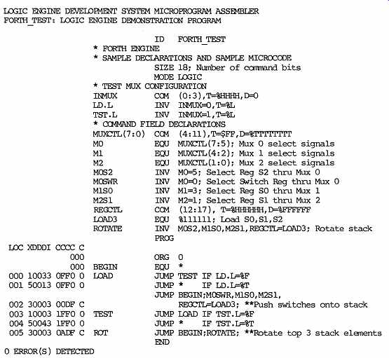
FIG. 17 Microcode for the design example.
LEASMB microprogram statements have an optional label field, an operation field, and an optional operand field, in that order. Within the operand field, the required subfields are separated by semicolons; comments may follow the operand field, if preceded by a semicolon. Lines beginning with an asterisk are comments.
An LEASMB output listing, such as in FIG. 17, shows the source program and, to the left of the program phase, the object code in hexadecimal notation.
An LEASMB program begins with the directive ID and ends with the directive END. The ID is the name assigned to the object code produced by the assembler, END marks the physical end of the program text. The declarations precede the program; the directive PROG separates the two. In the declaration phase, the directive SIZE specifies how many command bits are used in the design. The directive MODE, which takes an argument LOGIC or VOLTAGE, announces how the assembler is to interpret numeric data that could describe either logical or voltage values. As mixed logicians, we choose LOGIC mode.
Unless otherwise specified, numbers are in decimal notation. Binary constants are preceded by %, and may contain numerals 1 and 0, logical T and F, or voltage Hand L.
The declaration phase has three main directives: COM, INV, and EQU. The program phase has, besides mnemonics for each of the 2910 sequencer's instructions, two directives: ORG and EQU. COM specifies the nature of the command bits in the microinstruction; INV allows a symbolic name to invoke complex operations on command bits; EQU allows the equivalencing of names to values or to other names. ORG declares the origin of the microinstructions in the control store.
Command bits, presented to the architecture by the command field of the pipeline register, are defined by the COM directive. In FIG. 17, the definition of REGCTL provides the following information: REGCTL is a field of 6 bits which occupy bits 12 through 17 of the command field of the microinstruction.
[If we choose, we may refer to individual bits or groups of bits of REGCTL using a default set of indices, 0 for the leftmost bit through 5 for the rightmost bit. Thus REGCTL(0:3) would reference the leftmost 4 bits of the field. This notation frees the programmer from a dependence on the positions of particular command bits.] For each bit of REGCTL, truth is represented by a high voltage level (T = %HHHHHH). Whenever any bits of REGCTL are not mentioned in a microinstruction, the default values will be false (D = %FFFFFF). (A microinstruction will usually deal explicitly with only a few command bits; the default declarations of command bits are therefore of great importance in freeing the programmer from unnecessary details. In this example, the default values hold the current contents of the stack registers.)
The MUXCTL(7:0) declaration specifies that MUXCTL occupies bits 4 through 11 of the command field. In our program we may refer to individual bits or groups of bits using indices 7 (for the leftmost bit) to 0 (for the rightmost). This explicit indexing notation overrides the normal default notation. For each bit of MUXCTL, truth is represented by a high voltage (T = %HHHHHHHH). By convention, their unspecified default values are false.
In our illustration, we usually wish to deal with the group of command signals that controls a particular multiplexer in FIG. 15. So, for convenience, we define three variables MO, Ml, and M2 in the next three lines of the program.
MO is declared to be a field of 3 bits, equivalent to bits 7 to 5 of MUXCTL. Similarly, Ml and M2 are declared to be equivalent to bits 4 to 2 and bits 1 to o of MUXCTL. With these definitions, we may refer to the field MUXCTL as a whole or to subfields MO, Ml, and M2, or to any bit or group of bits of MUXCTL. These uses of the EQU directive equate names with fields. EQU may also be used to equate names with values or with addresses. LOAD3 is defined with an EQU as equivalent to the binary pattern %111111. BEGIN is defined in the program phase as equivalent to *. Since * in this context designates the current assignable control-store address, this notation equates the symbol BEGIN to the address 000. In examining FIG. 15, you will see that, in order to select stack element SO as the output of multiplexer 1, we must present the code 3 (binary %011) to the MUXI select inputs. For convenience, we define a symbol MlS0 that will invoke (INV) the value 3 on the field M1. If we wish to pass element SO through MUXI, we write MlS0, thus assigning the value 3 (%011) to the field Ml in the microinstruction. In the microcode in FIG. 17, the instruction at location 002 illustrates this usage. The symbol ROTATE illustrates how we easily may develop complex invocations. The use of ROTATE in the instruction at location 005 invokes the previously defined invocations MOS2, MlS0, and M2S1, and invokes the value LOAD3 in the command bits defined for REGCTL. Invocations are the most important concept in LEASMB; they are the key to achieving high level specifications of our microinstruction operations.
The microprogram performs two operations: loading the contents of the display panel's switch register into stack element SO (and simultaneously pushing the stack down), and performing a cyclic rotation of the top 3 elements of the stack. Two pushbuttons on the display panel, LD and TST, control the actions.
When LD is pressed and released, the load-and-push operation will occur; pressing and releasing TST will cause the execution of the rotate operation. It is necessary to assure that the microcode for loading and rotating will be executed only once for each push of the button. The code at locations 000 and 001 performs a single-pulser function for the LD button; the code at location 003 and 004 performs a similar function for the TST button. From the discussion in section 6, you can see that in our microcode we have developed pure-control versions of the single-pulsers. We return for a closer examination of this structure later in this section.
When the instruction at location 003, JUMP LOAD IF TST.L=%F, is executed, test input signal TST.L must be selected through the designer's test multiplexer, and a false value of TST.L must cause a branch to microinstruction LOAD. In the declaration phase, the command variable INMUX describes the select signals for the test multiplexer. The declaration of the variable TST.L specifies that TST.L will invoke the value 1 for INMUX. This agrees with Fig. 16, in which TST.L appears at input position 1 of the test multiplexer.
Test signals entering the test multiplexer may be represented as T = H or T = L, like LD.H and TST.L. A jump may be desired for either a true or a false value of a test signal, as in the microinstructions at locations 000 and 001, or at 003 and 004. The LEASMB microassembler arranges for the correct voltage to be presented to the 2910's CC input, in accordance with the specifications in the program's instructions and declarations. The designer declares the voltage conventions once and may thereafter deal with signals as logical entities. In our example, the declaration of TST.L has a term T = %L appended to an otherwise normal invocation. This declares that if a microinstruction ever specifies TST.L as the source for the 2910's CC input, then truth is represented as a low voltage level. The microprogram sequencer portion of an LEASMB microinstruction contains a bit, set by the assembler, that specifies whether the incoming test voltage should be inverted before it enters the 2910. (In exercises at the end of the section, you are asked to ascertain from FIG. 17 which bit of the micro instruction corresponds to this CC-inversion flag, and what voltage transformations are induced by the instructions in the microcode.) Use this informal description of the language to follow the test program.
In the Logic Engine's microassembly language, we have tried to encourage the use of high-level structured coding within a simple syntax. Let us now return to the design of our Forth Machine circuit.
Testing the System
Using the command-bit structure declared in the microprogram, we wire the appropriate bits of the Logic Engine's pipeline register to our architecture. We assemble the test microprogram and load it into the Logic Engine's WCS, making the appropriate monitor commands. We clear the Logic Engine, thereby causing the next microinstruction to be taken from location 000. Feeling bold, we enter the automatic run mode, causing the Logic Engine repeatedly to execute the instructions at locations 000 and 003, waiting for us to press the LD or TST pushbuttons on the display panel. We put a desired value into the display panel's switch register, and press and release the LD button. Assuming that we have wired the outputs of the stack elements to the LEDs on the display panel, we may observe the results directly on the panel.
If, as is likely, there is some problem with the behavior of the load-and push operation, we must debug the architecture and the code. The single-step mode is useful at this point; it allows us to execute our microcode yet freeze the system after each instruction so that we may observe the status of any signals in the architecture. Breakpoints are also useful, to suspend the execution of microinstruction. In debugging larger microprograms, a combination of breakpoint and single-stepping is a powerful aid to the designer.
If we isolate a problem and wish to supply a particular set of commands to the architecture, we may use the monitor's manual-execution mode, in which we present manually generated command-bit patterns for loading into the pipeline register. During manual execution, we may (in fact, must) specify whether we wish the Logic Engine to issue a clocking signal to our architecture. We have detailed control of the entire debugging process. If we determine that a particular microinstruction is incorrect and the error does not warrant a reassembly of the program at this time, we may manually change the microcode in the WCS. Without all this assistance from the development system, the designer would find it very difficult to express the control algorithm and debug the design.
Now we are ready to study a more complex microprogrammed design.
DESIGNING A MICROPROGRAMMED MINICOMPUTER
With the aid of powerful development facilities such as those provided by the Logic Engine, we are in a position to tackle a more difficult problem. You have already studied the LD20 hardwired minicomputer in sections 7, 8, and 9; in this section we will borrow its architecture and will develop a microprogrammed version of the control algorithm. We call the new design the LD30. Although the execution will be slower, the development of the LD30's control algorithm will be vastly simpler than the hardwired algorithm of the LD20. Nevertheless, to accomplish a microprogrammed implementation of this magnitude will require the use of all the sophisticated development aids offered by the Logic Engine.
Developing a Microprogram
The following prescription is useful for developing the microprogram:
1. Develop the main architecture. For our LD30, we would follow almost identically the path taken in section 7, and we will adopt the LD20's main architecture.
2. Specify the obvious command bits for controlling the architecture. We need not worry about details at this stage, but our knowledge of the architecture will give us much insight into the commands needed to control it. We may modify our list of commands later.
3. Write high-level microinstructions for the control algorithm. We will use the Logic Engine's microassembly language, which will allow us to express complex operations in symbolic terms without going into details. Since we have already studied the elements of the control process for the LD20, we can draw on this experience, using notations that are as close as reasonable to those used in the LD20's ASM chart.
4. Develop the declaration phase of the microcode. This is primarily the specification of invocation variables to expand in ever-increasing detail the high-level notations used in the microinstructions.
5. Tidy up. Complete the details of command-bit representations, test inputs, minor architectural elements, and definitions of the behavior of specific chips used in the architecture.
The Architecture of the LD30
We adopt almost intact the architecture developed for the LD20. FIG. 18 shows one of the twelve bit-slices in the main data structure. We see the principal registers, the ALU, and the main bussing system for the 12-bit data of the LD30.
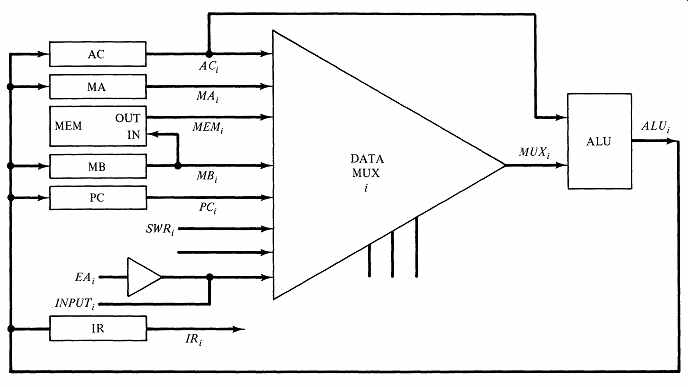
FIG. 18 The main data paths of the LD30.
We will use the LD20's structure for the accumulator and link; this is shown in FIG. 19. Also, we will use the LD20's structure for the memory and its controller. We anticipate that the LD20's state generator will be completely missing from our microprogrammed implementation, since the microprogram controller in the Logic Engine performs the next-state selection. We expect our LD30 to contain at least one new architectural element: the test multiplexer that supports the delivery of the specified test signal to the microprogram controller.
We will specify other architectural elements as we encounter them in developing the control algorithm for the LD30.
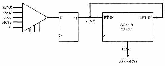
FIG. 19 The accumulator and link of the LD30.
A First Approximation of the Command Bits
To provide a concrete point of reference for our later work, it is useful to specify as many of the architecture's control signals (the microinstruction commands)
as are evident from the LD30's present architecture. This step could be deferred, since at this point it is just an approximation, but we have learned to appreciate having this early anchor to reality. As we pursue a top-down design, this knowledge can keep us from generating interesting but unproductive microcode.
Our first attempt to define control signals for our LD30 might take the form of TABLE 3. At a rough guess, we expect to have to test around 30 input or status signals; 5 or 6 bits will probably be required for the test multiplexer's select code. The controls for the data mux, the ALU, and the principal data registers are the same as in the LD20. The link multiplexer and the memory controls are also carried over from the earlier work on the LD20.
TABLE 3 PRELIMINARY COMMAND SIGNALS FOR THE LD30
We expect to need additional architectural elements for our LD30's interrupt control, input-output control, Operate instruction priority control, and the halting operations, but we are not yet clear about their nature.
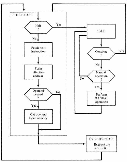
FIG. 20 LD30 control.
Writing the High-Level Microcode
We will use our earlier analysis of the LD20's control algorithm (see section 7) to help develop the LD30's microcode. The hard work-understanding the PDP-8's specifications well enough to describe a correct control algorithm-is the same for the microprogrammed LD30 as for the hardwired LD20. In the LD20, we expressed the algorithm as an ASM chart. For the LD30, we will use the Logic Engine's LEASMB microassembly language. The two versions differ dramatically in appearance-the ASM chart is a two-dimensional flow diagram, whereas the microassembly language is linear, like a computer program.
The two versions also differ in detail, since the LD20's ASM contains many states with multiple tests (multiple qualifiers) and conditional outputs, which are not permitted in the single-qualifier microinstructions supported by the Logic Engine. And the implementations of the two control algorithms are wildly different.
However, the overall sequencing should remain the same. We do not need an ASM for our work on the LD30, but to tie this work more closely with the LD20, we will use LD20 nomenclature when practical. FIG. 20 is a high level diagram of the LD30's control algorithm. The algorithm consists of four principal blocks: the fetch phase, the execute phase, the idle phase, and the manual phase. We must decompose each block into a sequence of microinstructions. As always, we will strive for a top-down development.
The Idle Phase of the LD30
The purpose of the idle phase is to detect an operator's action at the LD30 display panel. As in the LD20, we must take care to process only synchronized input signals in our algorithm, and we must provide a means of processing each depression of a pushbutton on the display panel only once.
We may contemplate the use of a flip-flop HALTFF to record the status of halt requests, as we did in designing the LD20. A request to halt will eventually cause the algorithm to reach the idle phase; we should be prepared to clear the halt request at this time. The addition of a HALTFF flip-flop to our architecture will require appending two command bits to our list (for controlling J and K in a JK flip-flop or D and its enable in an enabled D flip-flop). In the LD20 a composite signal MANSW* indicates the assertion of at least one pushbutton signal. MANSW* is the input to a single-pulser whose output is MANPULSE. MANPULSE is synchronized with our system clock and assures that a depression of a pushbutton is responded to only once. Following the discussion of single-pulsers in section 6, we can envision several implementations of the MANPULSE signal.
Figure 21a shows an architectural implementation of MANPULSE, involving the two flip-flops and an AND gate that we have come to expect of this circuit. In this circuit, the microcode for the LD30's idle phase might be:
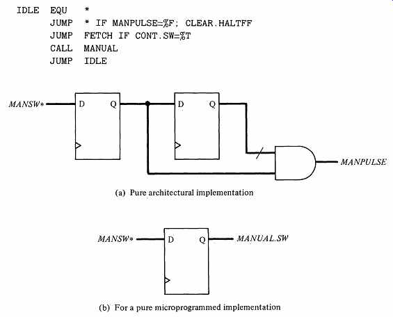
FIG. 21 Two versions of the hardware for the LD30's single-pulser. (a)
Pure. architectural implementation (b) For a pure microprogrammed implementation
From section 6, we learned that the single-pulser could be expressed as a pure algorithm rather than as an architectural element. In hardwired design, both views result in the same circuit. In microprogrammed design, the algorithm is expressed as microcode, and is never reduced to a hardwired circuit. Thus, we may implement the LD30's idle phase using a single flip-flop to synchronize the asynchronous signal MANSW*, as shown in FIG. 21b and in the following microcode:
IDLE EQU * JUMP * IF MANUAL.SW=%T; CLEAR.HALTFF JUMP * IF MANUAL.SW=%F JUMP FETCH IF CONT. SW=%T CALL MANUAL JUMP IDLE
The first instruction jumps in place until all buttons are released, thus assuring that any previous depression of a pushbutton is processed only once. The next step is to hang up until the operator depresses a pushbutton, which then allows the idle phase to proceed. This second procedure is superior, since it requires less hardware and only one additional microinstruction. This form of single pulser was used in our Forth Machine design example.
As we did in the LD20, we will insert into the architecture the large OR gate necessary to produce MANSW* from the collection of individual pushbutton signals on the display panel. We could dispense with this OR gate by writing microcode that serially single-pulses through the individual pushbutton signals, but this would require synchronizing each signal separately and would generate much additional microcode.
The Manual Phase of the LD30
The processing of manual operations in the LD20 was rather tedious, since the manual operations were merged with the execute phase. In the LD30, the manual phase is much more straightforward, as the following microcode shows:
[...]
This microcode employs a sequential test of each pushbutton; if one is depressed, a subprogram is called to process it. A typical operation such as SWR.TO.MA must cause the transfer of the switch register to the selected register, in this case the memory address register. At this stage, we are unconcerned with the details of this transfer, other than to realize that, in our architecture, it can be performed in one clock cycle. Later, we will expand SWR.TO.MA and its cousins into the proper command-bit assertions, but now we do not permit these details to interrupt our thoughts.
Writing into memory requires the presentation to the memory buffer register of the data to be written, followed by an execution of a standard memory-write subprogram. We may specify the details of the WRITE subprogram at our convenience, but to satisfy your curiosity, we will do so now:
WRITE EQU *
CONT START.WRITE
JUMP * IF CC=%F
RTN
Using the standard memory protocol of the LD20, we issue a START. WRITE signal (one of our two memory command signals) and wait until the cycle complete response CC becomes true.
We've completed the microcode for the idle and manual phases. Next comes the instruction-fetch phase.
The Fetch Phase of the LD30
The conversion of the fetch phase of the LD20's ASM to our microprogrammed version is straightforward:
This microcode calls on several subprograms that are as yet unspecified: INTERRUPT.TEST, READ.TO.IR, READ.TO.MB. The memory-read subprograms are short, and we will elaborate them here; the treatment of INTERRUPT. TEST will appear later.
In section 7, developing the fetch phase was rather complex but now that we understand it, rendering our understanding into microcode is simple. As always, we have made good use of our ability to describe each microinstruction in high-level terms.
The Execute Phase of the LD30
At the start of the execute phase, IR will contain the current instruction, MB will contain any needed operand from memory, and MA will contain the effective address EA, if required. For the execute phase, we must develop microcode to decode the instruction and perform each type of PDP-8 operation. Given our work on the LD20, the execution of most of the instructions is straightforward, and we might proceed as follows; some of the details are left for you to complete.
[...]
In the TAD.CODE block, the development of the arithmetic sum is caused by the execution of the ADD.MB.TO.AC invocation in the first microinstruction.
The result of the addition, both the sum and the carry-out status, are available during the instruction. At the end of the instruction, the sum is loaded into the AC. During the instruction, we test the carry-out signal ALU.COUT, and if it is true, we arrange to complement the link bit.
The microcode for the execution of three of the PDP-8's instructions is left to you to complete. Of the algorithm for the LD30's execute phase, there remain only to specify the code for the Operate and IOT instructions, deal with interrupts, settle on how we will decode instructions, and clean up a few loose ends.
The Operate instruction. In designing the LD20, we developed a sophisticated method of saving clock cycles in the execution of the PDP-8's Operate instructions. Microprogrammed control, although allowing much parallel activity in each microinstruction, is inherently more serial than hardwired control. The elaborate priority-detection system of the LD20 usually saved a few cycles (and served as a good illustration of priority circuits), but attempting a similar scheme in our inherently slower LD30 would be misplaced effort. We resign ourselves to plodding serially through all the possible operations within each group of the PDP-8's operate instruction. Let's assume that the decoding of the instruction, in addition to detecting the Operate instruction, has also identified the subgroup.
This is an arbitrary but reasonable choice, and it will fit right in with the elegant scheme to be discussed later.
A reasonable microcode for a part of the PDP-8's Operate instruction might then be as follows:
In problems at the end of the section, you are asked to complete the microcode for the Operate instruction, IOT Instruction. The PDP-8's IOT instruction performs input and output operations. As in the LD20, our LD30 must arrange for the signals IOP1, IOP2, and IOP4 to be asserted, if requested, long enough to examine the values of the incoming status signals IOSKIP, ACCLR, and ORAC. This examination will require several microinstructions, during which the appropriate IOP signal must remain solidly asserted. We could write brute-force microcode for this problem, with code to test the status of each of the three IOP signals. However, our choice is to introduce an element into the LD30's architecture to generate and maintain the IOP signals as required. We have already seen such an element in the LD20: the IOP signal enabler. This circuit has a 4-bit shift register that allows the enabling of each IOP signal in turn. We will use this circuit in our LD30. The microcode for the IOT instruction must then loop three times over the status tests-once for each of the possible IOP signals.
We use the 2910 sequencer's internal counting instructions to manage the looping.
[...]
The IOT instruction provided two suboperations ION and IOF for enabling and disabling the interrupt system. The suboperations are distinguished from
regular IOT instructions by a zero device address in IR3-IR8. The microcode for these operations is:
[...]
FIG. 22 Architecture of the interrupt system in the LD30.
Interrupt Processing in the LD30
The LD30 must be able to detect an interrupt request and present a synchronized version of the request to the microprogrammed control algorithm. The PDP-8's interrupt protocol also requires that we be able to determine if interrupts are enabled. If an interrupt is to occur, we must be able to force the execution of a CALL 0 instruction. For these functions, we adopt the same architectural elements used in the LD20. We show the architecture for the interrupt system in FIG. 22.
Handling an interrupt request began early in the fetch phase with a subprogram call to INTERRUPT. TEST. At the time we wrote that call, we had no clear idea how interrupts would be handled. Now, having made some architectural commitments to generate the INTERRUPT.REQUEST and INTERRUPT.ENABLE signals, and to finesse the awkward problem of generating a CALL 0, we are able to specify the microcode fully.
[...]
We called the interrupt-test code as a subprogram. If no interrupt occurs, the INTERRUPT.TEST microcode returns to the subprogram caller. If an interrupt occurs, the algorithm enters the regular execute-phase microcode, which is not a subprogram. Then, the code never makes a normal subprogram return back to the fetch phase, so we must take care to adjust the 2910 stack to remove the unused return point. The 2910 operation CJPP in the pass mode accomplishes both a jump and a stack pop.
Instruction Decoding in the LD30
The microcode for the execute phase calls a subprogram to decode the PDP-8 instruction residing in the IR. The operation code for most instructions is specified by the three bits in IRO, IR1, and IR2. Since our microinstructions can examine only one signal at a time, a pure microcode solution to instruction decoding is clumsy (although perfectly feasible). Here is a brute-force way:
[...]
In developing microcode for the execution phase, we decided that the instruction-decoding step would distinguish the three groups of Operate instructions and the two special cases of the IOT instruction. We could complete this decoding with further tests of additional bits of the LD30's IR, although the test for the IOT-instruction special cases of the IOT instruction is complicated by having to identify a 6-bit field of zeroes in bits IR3-IR8. All of this microcode is a serialized version of a basically parallel function-the decoding of a several-bit code. We already know that combinational logic, implemented with gates, decoders, or ROMs, can achieve rapid decoding.
We may simplify the decoding of LD30 instructions and illustrate some powerful control techniques by developing a solution that mixes architecture and algorithm. The 2910, at the heart of the Logic Engine's microprogram controller, normally expects to receive its D input from the microinstruction pipeline register; 14 of the 2910's 16 operation codes assume this. However, for the 2910's JMAP instruction, the D input comes from a different source, usually from a "mapping ROM." Let's use a ROM to assist the decoding.
Our goal is to examine bits of the LD30's IR and branch within our control microcode to the proper code for executing each type of PDP-8 instruction. The decoding of the PDP-8's basic instructions and our special cases requires examining all 12 bits of the IR. A pure ROM solution would use ROMs with 12 address inputs to produce about a dozen microcode addresses. However, many of the bits of the IR are needed only to detect the two special cases of the IOT instruction, ION and IOF. Our plan is to incorporate two signals in hardware: IOT.ION will be true for the interrupt-enable suboperation; IOT.IOF will be true for the interrupt-disable suboperation. For now, we assume the existence of these two signals; we will discuss how to create them later.
TABLE 4 DECODING THE LD30'S INSTRUCTIONS
Now the inputs to our instruction-decoding ROM are considerably simplified.
We require IRO, IRI, and IR2 to decode the main operation code; IR3 and IRll to distinguish the Operate instruction groups; and IOT.ION and IOT.IOF to identify the IOT subinstructions and to distinguish ordinary input-output IOT instructions from the special cases. These 7 signals form the inputs to the ROM; the ROM's output must produce microcode branch addresses that we can use to transfer to sections of the microprogram dealing with the PDP-8's 12 instructions and subinstructions. What are the 12 microcode branch addresses? From our microcode for the execute phase we see examples such as AND.CODE, IOT. CODE, and OP.G2.CODE. But the experienced microprogrammer will recognize a pitfall: the actual addresses of these locations in the microprogram memory depend heavily on the details of the microcode. If we modify the microcode, the likelihood is that a reassembly of the microcode will change the addresses of the subprograms. We certainly do not desire to reprogram our ROM every time we reassemble the LD30's control microprogram! To avoid this difficulty, we introduce a jump table into our microprogram. This table will be in a fixed location in the microinstruction memory, and we will guarantee not to alter its location. The ROM's outputs will point to entries in this jump table, and the table entries, from their fixed locations, will jump to the subprogram addresses. The advantages are great: the contents of the ROM remain fixed even though we modify the microcode, and our micro-assembler will handle the drudgery of locating the subprograms. TABLE 4 shows the structure of the mapping ROM and the microcoded jump table. If speed of execution is sufficiently important, after the design is ready for production you may program a new mapping ROM to point directly to the instruction execution code, thereby eliminating the microcoded jump table.
With the addition of the mapping ROM for decoding instructions, we may now write the DECODE.INST microcode whose existence we assumed when we developed the original microcode for the LD30's execute phase:
DECODE.INST EQU *; instruction decoding
JMAP ;; jump to correct instruction processing code
Declarations for the LD30 Control Microprogram
We have developed the main elements of the LD30's architecture and specified the control algorithm in high-level terms. Now we will develop the declaration phase of the microcode, in which we will expand our high-level invocations into actual command signals directed to the LD30 architecture.
Consider operations involving the main data paths. If we scan the executable instructions in the microprogram, we can catalog a large number of operations on the main data path. PC.TO.MA, CLEAR.AC, ADD.MB.TO.AC, and SWR.TO.IR are examples. In our version of the microcode, there are 27 different invocations that refer to the main data path architecture. These require selecting an operand through the data multiplexer, performing an appropriate ALU operation, and loading the result into some register. Still resisting the temptation to jump into the details of the hardware too soon, we break down each of these high level invocations into more detailed specifications:
[...]
We have tried to choose obvious names for the intermediate operations. For instance, SEL.MB means "select the MB register as the input to the ALU," ALU.PLUS means "cause the ALU to add its operands," and LOAD.AC means "load the AC with whatever is at its data inputs." At this stage, if we were to change our minds about some details of our main data path architecture, it is likely that these declarations would not require alteration.
Next, we must expand the specifications for each of the intermediate-level commands. Eventually, we will end up with detailed assignments of elementary signals to microinstruction command bits, but we need not hurry this process.
We may describe the data multiplexer selection codes as follows, using the same ordering of the multiplexer inputs as in the LD20.
[...]
We have described the selection of each input to the multiplexer in terms of its multiplexer select code. (As in the LD20, we have left data multiplexer input 4 unused, to allow for expansion. We have routed INPUT and EA, both controlled by three-state signals, into a single data multiplexer input. EA's control signal is ENABLE.EA, which will become one of the LD30's microinstruction command signals; INPUT needs no microinstruction command signal for its three-state control since that is governed by the PDP-8's input-output protocol.)
Now we can finally specify the details of DATAMUXCTL: it is a microinstruction command-bit field of 3 bits, as suggested in TABLE 3. Until we begin the wiring, the actual locations of the three bits are unimportant, even distracting.
We are nearly done. We may now tabulate the test input signals needed to drive the microcode, and prepare the necessary declaration statements. TABLE 5 contains the declarations. Each invocation describes the voltage polarity of the signal and its position within the test multiplexer.
TABLE 5 TEST INPUT DECLARATIONS OF THE LD30
This concludes our presentation of the development of the LD30's microcode declarations. The declarations tend to be lengthy, but they contain information important both for the microprogram assembler and for the reader of the microcode.
Properly specified, the declarations exhibit a gradual evolution of detail, from the high-level specifications in the microprogram algorithm down to the voltage behavior of each command line in the microinstruction. Later modification and maintenance of the design are greatly? simplified by the existence of this orderly, well documented record. We said earlier that the LEASMB invocation was the key to top-down design. Now you can see the power of this concept.
Our Design of the LD30 is Complete!
Our treatment of the microprogram for the LD30 is finished. We have shown representative portions of the algorithm and of the declarations that describe the terms used in the algorithm. How different is the LD30 machine from the LD20? The main elements of the architecture are the same in both the hardwired and microprogrammed designs. Several minor architectural features of the LD20 survive in the LD30, and the LD30 contains two major additions: the test input multiplexer and the jump-address EPROM used in instruction decoding. FIG. 23 shows the elements of the LD30's architecture. Not much is left.
The LD30 requires about 70 chips; the LD20, 125. The dramatic change between the two is, of course, in the implementation of the control algorithm.
In moving from the LD20's hardwired control to the LD30's microprogrammed control, we eliminate about 55 integrated circuit chips and innumerable wires.
The LD30's control algorithm looks like a program, and it is one. It contains about 120 microprogram instructions and several hundred lines of declarations.
Comments are often useful in the microprogram, but with well-chosen nomenclature and systematic top-down development, the microcode is largely self-documenting.
In the senior-level hardware laboratory at Indiana University, our students study, construct, debug, and extend the LD20 hardwired and the LD30 micro programmed versions of the PDP-8. With the aid of the Logic Engine, our students accomplish this in one semester, using wire-wrap technology. The proof of their performance is to download and execute actual PDP-8 programs-a source of immense satisfaction for the students and the instructors.
SUMMARY
Starting in 1964 with IBM's use of microprogramming in their System/360 digital computers, manufacturers have increasingly adopted microprogramming methods for the control of computers. It is fair to say that most computer designs now have at least some microcode in their control-a fact often unknown to the programmer, since the microcode is not visible. The conventional programmer works with the computer's machine or assembly language, or with higher-level languages, without being aware that there is really another layer of programming the microcode-buried in the hardware.
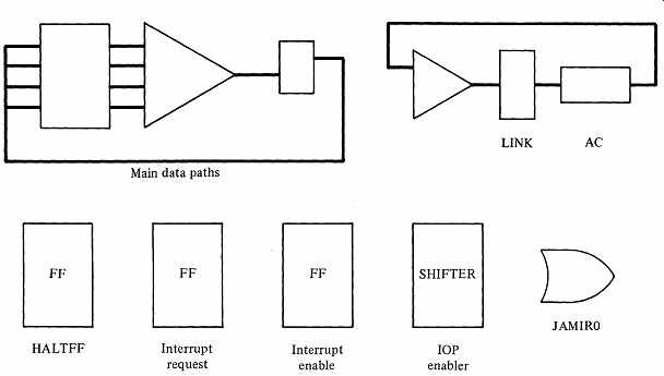
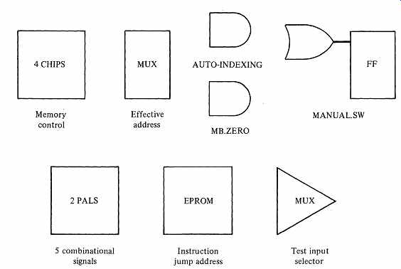
FIG. 23 Hardware elements in the LD30.
The great advantages of microcoding are its uniformity and ease of modification. Carrying the notion further, we could control all digital tasks with a single type of controller, such as a Logic Engine. Using microcode, we make the controller perform a specialized task for each type of device, for instance executing the PDP-8's instructions in the LD30. With identical copies of the basic microprogrammable processor, we could control computers, line printers, card readers, floppy disks, terminals, and other devices having suitable speed requirements. Each of these would have its own architecture, which would include the device itself and the logic needed to interface with the microcode.
Each controller would have its own microcode to control the architecture.
This has great potential advantages for both the designer and the maintenance engineer. The designer develops control algorithms with a uniform style, in a programming mode, using support systems derived from experience with software.
The maintenance engineer would have to master only one type of control hardware.
Each device's specialized control algorithm could be dealt with as a microprogram, a form that is generally easier to understand than a hardwired design. Diagnostic and documentation aids based on software principles can greatly speed both the development and the maintenance processes.
Unfortunately, although computer manufacturers make extensive use of proprietary microprogrammable processors, few general-purpose microprogramming systems such as the Logic Engine are available commercially.
In this section, we have discussed some basic principles of microprogramming and have shown how the concepts may become a powerful tool for design, requiring sophisticated support systems. We have not attempted to discuss the wide variety of microprogramming techniques; for this you may consult more specialized tests, such as those listed in the Readings and Sources.
Microprogramming is a great stride toward bridging the gap between hardware and software. Let us now move all the way, to the use of small conventional computers, microcomputers, as digital controllers.
EXERCISES
1. Describe Wilkes's great contribution to the systematic development of control algorithms.
2. Produce a Wilkes implementation similar to FIG. 3 for the ASM.
3. Produce a Wilkes implementation similar to FIG. 3 for the ASM.
4. Explain the meaning of "microprogram."
5. How does a ROM implementation of an ASM differ from Wilkes's implementation? In what ways is the ROM method less flexible?
6. In microprogramming terminology, what is a "qualifier"?
7. Produce a ROM-based multiple-qualifier microprogrammed implementation of the ASM.
8. Produce a ROM-based multiple-qualifier microprogrammed implementation of the ASM.
9. Sketch a representative part of a ROM-based multiple-qualifier implementation of the Black Jack Dealer ASM .
10. Discuss the advantages and disadvantages of the following methods of ROM-based microprogramming design. Consider the ease of implementation, generality of ASM structure, understandability of the result, ease of use, and so on.
(a) Multiple qualifier.
(b) Single qualifier, two addresses.
(c) Single qualifier, one address.
(d) Single qualifier in a Logic Engine environment.
11. Produce a single-qualifier, single-address microprogram implementation of an appropriate modification of the ASM. For this task you must alter Fig. 5-13 to accommodate the requirements of the microprogram. State clearly any assumptions you make in producing the altered ASM.
12. Perform Exercise 11 for the ASM.
13. Design a controller for single-qualifier, two-address microinstructions. The controller should support up to 256 microinstructions, up to 32 test inputs, and up to 40 command outputs. Specify the MSI chips that you use.
14. Perform Exercise 13 for a controller to execute microinstructions of the form of FIG. 8.
15. Why does the text's single-qualifier method not permit conditional outputs? Design a single-qualifier microinstruction interpreter that supports conditional outputs.
16. Complete the specification of the microcontroller in Fig. 10.
17. Characterize microprogrammed design as seen by:
(a) The hardware designer.
(b) The computer programmer.
18. Why is the hardwired control described in ASM charts not the best tool for the design of large, complex systems?
19. Propose a Logic Engine implementation of the Black Jack Dealer's control algorithm of Fig. 9. Express the microcode in the style of the Logic Engine's microassembly language described in the text.
20. Although RAM is appropriate for storing microcode in the Logic Engine during the development and debugging of an algorithm, why might RAM not be the best choice for a production version of a microprogrammed controller? On the other hand, what advantages might RAM-based microprogram storage have in a production version?
21. Compare the LD20 and LD30 as to speed, number of states, total design effort, and anticipated ease of maintenance.
22. The text mentions an early microprogram sequencer, the 2909 4-bit sequencer slice. To achieve a realistic number of microprogram address bits, several of these chips are to be cascaded together. What connections do you anticipate will be required between the cascaded 2909 chips?
23. Look at Fig. 17, which contains the microcode for the Forth Machine design example. The object code is presented in hexadecimal notation, with 4 bits per hexadecimal digit. In the object code, 1 represents a high voltage and 0 a low voltage. One of the bits in the X field of the object code is the 2910's CCEN input. The Logic Engine implements an unconditional jump by making CCEN false, thereby forcing a pass operation in the 2910. A conditional jump, which makes use of the 2910's CC input, requires CCEN to be true.
(a) By inspection of the object code in Fig. 17, determine which bit of the X field is CCEN. (b) State whether the 2910's CCEN is high-active or low-active.
24. Another of the X-field bits in the Logic Engine microcode of FIG. 17 is CCINV, the assembler's specification that the voltage of the incoming test signal must be inverted in order that the 2910 properly interpret the signal. The 2910's CC input is low-active.
(a) By inspection of the object code, determine which bit corresponds to CCINV.
(b) Using the declaration for LD.L and TST.L, determine the correct status of the CCINV bits (true or false) in the microinstructions at locations 000, 001, 003, and 005.
(c) Determine if CCINV is high-active or low-active.
25. From FIG. 17, expand the hexadecimal digits for the command bits in the object microinstructions at locations 001 and 002, so that you can observe the 18 command signals individually. For each of these microinstructions, verify that the bits in the object code are consistent with the declarations in the source program.
26. In FIG. 17, why is the curious term T=%L appended to the declarations for LD.L and TST.L?
27. Complete the LD30 microcode for the following PDP-8 instructions: (a) AND. . (b) DCA. (c) JMP.
28. Complete the LD30 microcode for the parts of the PDP-8's Operate instruction not elaborated in the text:
(a) Group 1.
(b) Group 2.
29. Exercise 8-52 requires the addition of the PDP-8's Group 3 instructions to the LD20's hardwired design. Repeat that exercise for the LD30, showing all modifications or extensions of the architecture and the microcode.
30. Consider the PDP-8's IOT instruction. Assume that the IOP signal enabler is eliminated from the LD30's architecture. Implement the IOT instruction solely in microcode. Remember to keep each required IOP signal asserted throughout the testing of the incoming status signals.
31. Explain clearly why we chose to implement the decoding of the LD30's instructions with a mapping ROM and a separate jump table rather than by using the faster method of having the mapping ROM jump directly to the appropriate microcode.
32. From the LD30 microcode given in the text, find ten examples of operations on the main data path, other than PC.TO.MA, CLEAR.AC, ADD.MB.TO.AC, and SWR.TO.IR. Write LD30 invocation declarations for your ten operations, following the examples in the text. Expand any intermediate operations until each element is finally reduced to command declarations.
33. Perform Exercise 8-50 using the LD30's microprogrammed design. Show modifications or additions to the architecture and microcode.
34. Perform Exercise 8-51 using the LD30's microprogrammed design. Show modifications or additions to the architecture and microcode.
35. Perform Exercise 8-52 using the LD30's microprogrammed design. Show modifications or additions to the architecture and microcode.
36. Perform Exercise 8-53 using the LD30's microprogrammed design. Show modifications or additions to the architecture and microcode.
37. Choose a computer of your choice, such as the PDP-ll, M6809, M68000, or Intel 8080, and write a microprogram to implement the processor's instruction set. Use the style of the Logic Engine's microassembly language. The suggested processors are complex, and you may wish to consider a subset of the instructions. The user's manual for your chosen processor will probably not give much insight into the internal organization of the processor. As we did with the LD20 and LD30 versions of the PDP-8, start with the instruction set and the obvious registers referenced by the instructions. You are free to specify additional registers, data paths, and control signals required to achieve your implementation.
38. Propose a Logic Engine implementation of the Black Jack Dealer's control algorithm of FIG. 10. Express the microcode in the style of the Logic Engine's assembly language described in the text.
Related Articles -- Top of Page -- Home