AMAZON multi-meters discounts AMAZON oscilloscope discounts
To make the LD20 truly useful, we need to be able to attach input and output devices to it. In this section, we will design an asynchronous interface between a keyboard-display terminal and the LD20. The interface will support the execution of PDP-8 IOT instructions designed for controlling the terminal. We will first describe the terminal device and its communication mechanism. Then after reviewing the PDP-8 input-output protocol, we will describe the specific IOT instructions for the terminal. With this background, we will design the interface.
The design will follow the usual pattern of separating architecture and control, but we will develop an asynchronous ASM for the control section of the interface.
TERMINAL COMMUNICATIONS
A typical terminal consists of a keyboard and a display which communicate with other devices over two pairs of signal wires. One pair of wires transmits data from the terminal; the other pair receives data into the terminal. The terminal transmits and receives data serially, one character at a time. Each character is itself sent serially, I bit at a time, at a set rate, typically 300 to 9600 bits per second. The terminal transmits and accepts characters in an 8-bit code: usually the 7 -bit ASCII character code plus an eighth bit that sometimes represents character parity. Data is transferred using the standard asynchronous communication discipline, which sends each character as a self-contained entity. In this discipline, a signal line has two valid levels: mark, corresponding to a data I-bit, and space, corresponding to a data 0-bit. When no data is being communicated, the signal line is in the mark level. To begin transmitting a character, the transmitting device changes the signal level from mark to space, and holds the space level for one bit-time. This creates a start bit for the character. After the start bit, the 7 ASCII character code bits and the eighth (parity) bit follow, each occupying one bit-time. Following the eighth bit are one or two stop bits, in the mark level. FIG. 1 shows the waveform for the asynchronous trans missions of the ASCII character "P," which has the code 1208 • We assume that the parity bit records even parity for the 8 data bits; in the example we use one stop bit. A character requires 7 data bits, 1 parity bit, 1 start bit, and 1 stop bit, for a total of 10 bits per transmitted character, making the maximum rate of character transmission one-tenth of the transmission bit rate.
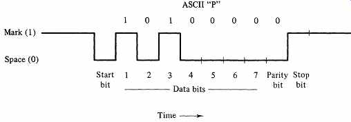
FIG. 1 Asynchronous transmission of the ASCII character "P." Even
parity, 1 stop bit.
The receiving device detects the start bit by observing the transition from mark to space on its incoming data line, and then senses each bit as it arrives, at the agreed-upon data rate. Each character forms a packet of information independent of other characters.
THE PDP-8'S INPUT-OUTPUT PROTOCOL
The PDP-8's input-output protocol is specified by the IOT instruction, which is described in Section 7. The programmer may request that any of three IOP signals be sent to the external world, along with an address to identify the particular device. The PDP-8 (and our LD20) receives control information from the addressed device over the three lines IOSKIP, ACCLR, and ORAC. Twelve bits of data leave the computer from the AC, and 12 bits enter the computer over the LD20's INPUT lines. The external device must respond only when addressed, and then only according to the protocol established between that device and the PDP-8. The PDP-8's protocol specifies the sequence for delivering IOP signals, and for processing the incoming control signals.
Our principal concern in this section is to design an interface between a keyboard-display terminal and the LD20. The interface must reconcile the vast difference between the behavior of the terminal and the behavior of the LD20. The terminal will transmit and receive characters according to the asynchronous communication discipline, whereas the LD20 uses the rather curious input-output protocol implied by the PDP-8's IOT instruction.
The PDP-81 computer manual contains a set of elementary instructions for communicating with a simple keyboard-display terminal. Since we wish to use PDP-81 software, we must adopt the standard format of PDP-8 terminal instructions.
The PDP-8 interface has two device addresses: 03 (DA03) for receiving characters from the terminal, and 04 (DA04) for transmitting characters to the terminal.
Each of the three IOP signals plays a role in both transmitting and receiving data. Here are the IOT instructions for the PDP-8's standard interface with a terminal.
From Terminal to PDP-8 (DA03)
IOP1 (Instruction 60318 ). If there is a character from the terminal ready to be sent into the PDP-8, the interface must respond to the DA03 IOP1 signal with IOSKIP = T; at all other times, IOSKlP = F. This instruction allows the programmer to skip an instruction if incoming data is ready. If no new data is present, no instruction is skipped.
IOP2 (Instruction 60328), In response to the DA03 IOP2 signal, the interface clears its internal indication that a character is ready and sends ACCLR = T to the PDP-8. At other times, ACCLR = F. Asserting ACCLR causes the PDP-8 to clear the accumulator, anticipating the IOP4 exchange to follow.
IOP4 (Instruction 60348 ), When IOP4 = T, the DA03 interface places its incoming data (12 bits) on the external input lines INPUT to the PDP-8. The interface also issues ORAC = T to the PDP-8, which initiates the loading of incoming data into the previously cleared AC. Of the 12 bits of data supplied by the interface, the leftmost 4 are zeros, and the rightmost 8 contain the terminal data.
The programmer will usually combine IOP2 and IOP4 into one instruction (60368), The following is a simple input sequence for receiving one character from the terminal; the code begins at address 10048 ,
Store data from accumulator
IOP1 (Instruction 6041 8), If the DA04 interface can accept a character from the PDP-8, the interface must respond to the DA04 IOP1 signal with IOSKIP = T; otherwise, IOSKIP = F. This gives the programmer the ability to skip an instruction if it is acceptable to send a character to the terminal.
IOP2 (Instruction 60428 ), The transmit interface must clear its internal indication that the transmit stage is free, thus marking DA04 as busy. The interface remains in this condition until a character has passed through the transmit stage and the transmit stage can again accept a character.
IOP4 (Instruction 60448), This signal causes the DA04 interface to load a character of data from the lower 8 bits of the PDP-8's accumulator. The interface transmits these 8 data bits to the terminal, and having done so, marks the DA04 internal flag as free to accept another character.
The programmer will ordinarily issue IOP2 and IOP4 together in one IOT instruction. Here is a sequence for transmitting one character to the terminal; the code begins at location 1004:
Location 1004 1005 1006 1007 Instruction
6041 5205 6046 Load character data into accumulator IOT I,DA04: Skip if transmit unit is available JMP $-1: Wait until transmit unit is free IOT 2 + 4,DA04: Clear transmit flag, and send character
REQUIREMENTS OF THE LD20-TERMINAL INTERFACE
We have described the terminal and the PDP-8 instructions for reading and writing terminal information. Now we can specify our interface between the LD20 and the terminal. The interface has three responsibilities: to support input from the terminal to the LD20, to support output from the LD20 to the terminal, and to provide proper interrupt signals to the LD20.
Interface Flags and Interrupts
The interface must maintain a status flag for each device address. DA03FLG becomes true when the interface has a new character for the PDP-8; DA04FLG becomes true when the interface is able to accept a new character from the PDP-8. The PDP-8 programmer is responsible for resetting each flag to false, using appropriate IOT commands.
Whenever either flag is true, the PDP-8's external interrupt signal EXTINT* must be true. For a single terminal device, this means
EXTINT* = DA03FLG + DA04FLG
These two flags not only affect the PDP-8's external interrupt system; they are also the key to controlling the terminal operations using the IOT instructions.
The Receive Section (DA03)
The receiving section of the interface:
(a) Receives serial data from the terminal according to the asynchronous communication discipline, converts the data to an 8-bit parallel byte, and holds the byte for possible transmission to the LD20. (b) Keeps an internal receive status flag (DA03FLG) to inform the LD20 of the status of the receive station. The interface sets DA03FLG to true upon receipt of a complete character from the terminal. The LD20 programmer may set the flag to false with an IOT instruction that issues IOP2 with device address DA03.
(c) Recognizes DA03, and when DA03 is present responds to the LD20's signals IOP1, IOP2, and IOP4 with the actions described earlier. Device address 03 is (d) Issues T on the external interrupt line EXTINT* whenever DA03FLG is true.
The Transmit Section (DA04)
The transmitting section of the interface:
(a) Recognizes DA04, and when DA04 is present responds to the LD20's signals IOP1, IOP2, and IOP4 with the actions described earlier. Device address 04 is (b) Upon recognizing IOP4 with DA04, receives 8 bits in parallel from the LD20 and transmits these bits serially to the terminal, using the asynchronous communication discipline.
(c) Keeps an internal transmit status flag (DA04FLG) to inform the LD20 of the status of the transmit section. This flag becomes false when the LD20 program issues IOP2 with device address DA04. The flag goes true after the LD20 has written a character to the terminal and the character has passed through the interface sufficiently for the interface to be able to accept another character from the LD20. (d) Issues T on the external interrupt line EXTINT* whenever DA04FLG is true.
PRELIMINARY ARCHITECTURE OF THE INTERFACE
In Fig. 2, we show the signals between the LD20 and the interface, and between the terminal and the interface.
To build the interface black box, we could design a complete MSI serial to-parallel and parallel-to-serial system. However, 8-bit serial data transmission is common, and manufacturers have produced a device to assist in the conversion between serial and parallel data.
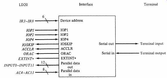
FIG. 2 Interface signals in the LD20-terminal interface.
The UART
The universal asynchronous receiver-transmitter (UART) is a complex LSI circuit in a 40-pin integrated circuit package. Several manufacturers produce functionally equivalent chips. The purposes of the UART are to receive data according to the asynchronous communication protocol and render it into parallel form, and to accept parallel data and transmit it serially according to the asynchronous protocol. The UART has inputs to specify the number of bits per character (from 5 to 8), the parity mode, and the number of stop bits; hence the name "universal." In our design these are fixed parameters, so we will not consider them further. Design Examples 3 and 4 in Section 6 illustrate the internal operations of a UART. The UART has independent serial receive and serial transmit sections.
Here is a description of the important UART signals. All signals are high-active (T = H) unless otherwise specified. (UART nomenclature is not standardized; check the appropriate data sheet for the names of signals, the direction of bit numbering in registers, and so forth.)
Signals of the UART's receive section
Receive Serial In (RSI): The serial data line from the terminal.
Receive Buffer Register (RBR8-RBRl): Outputs from an 8-bit register that holds an assembled character received from the terminal (bit 1 is on the right). These outputs are three-state.
Data Received (DR): A status flag that becomes true when a valid terminal character enters RBR. DR becomes false upon the F -? T transition of the DRR signal, described next.
Data Received Reset (DRR): A F -? T transition of this signal clears DR to false. This signal is low-active (T = L).
Receive Register Disable (RRD): The receive buffer register has three-state outputs that are disabled as long as RRD is true. When RRD = F, the outputs RBRS-RBRI are available for use.
Receive Clock: The UART expects a receiver clock input of 16 times the serial bit rate. A typical clock frequency is 1200 x 16 = 19,200 Hz.
Signals of the UART's transmit section Transmit Serial Out (TSO): The serial data line to the terminal.
Transmit Buffer Register (TBRS-TBRl): Inputs to an 8-bit register that holds a character prior to its being serialized to the terminal (bit 1 is on the right). Transmit Buffer Register Load (TBRL): Upon a F --> T transition on this line, the UART accepts an 8-bit character at inputs TBRS-TBRI. When the transmit data serializing section of the UART is free, the UART will then move the new character into the serializing section, thus freeing the TBR. This signal is low-active (T = L). Transmit Buffer Register Empty (TBRE): This signal is true whenever the UART can accept a character into the TBR. It is false when the TBR is full, awaiting access to the transmit data serializing section.
Transmit Clock: Provides clocking for the UART's transmit section. It has the same characteristics as the receive clock and will usually originate from the same external timing source.
Incorporating the UART into the Design
Using the UART will save us much design work. With it, we have transformed our main problem for interfacing the LD20 to the terminal into interfacing the LD20 to the UART-a much simpler task. We must now determine how to reconcile the LD20's input-output protocol with the UART's status and command signals. Before we can further specify the architecture of the interface, we must investigate the control algorithm for the interface between the LD20 and the UART.
THE INTERFACE CONTROL ALGORITHM
Clocking Events in the Interface
So far, the designs in this book have been synchronous, driven by a master clock whose effect was implied in the ASM chart but which did not explicitly appear. What is the clock for the LD20-terminal interface? We must supply a UART clock, but it is too slow (perhaps 19,200 Hz) to interface with the LD20, which runs a hundred times faster. Also, the UART's fixed clock rate violates our variable-clock-speed design criterion. The LD20 system clock would serve nicely, especially since most of the interface control information consists of IOP signals that are synchronized with the LD20's clock. However, the PDP-8's input-output protocol does not specify that the computer's clock is available to its peripheral devices.
Should we devise an asynchronous design? In Section 5, we sidestepped asynchronous methods in favor of synchronous design, which is easier to manage and has fewer pitfalls. Providing the interface with the LD20 system clock would allow a synchronous design-the easiest solution to our problem. However, to present the flavor of unclocked circuits, we will develop an asynchronous interface.
In asynchronous design, with no master clock to drive the system, states can change only when the test inputs change. What are the test inputs for our interface? The main tasks are recognizing the two terminal device addresses and then responding to the LD20's IOP signals. The start of an event in our algorithm will be the recognition of DA03 or DA04 and the assertion of an IOP signal. The event will last until the IOP signal becomes false or the device address changes. FIG. 3 is a partial ASM chart for the interface events.
In synchronous design, fluctuations in input signals cause no trouble provided that the inputs are stable at the clock transition. In an asynchronous circuit, the inputs act as clocks; any change in an input can produce ASM transitions, intended or accidental. This is the great difficulty with asynchronous design; the circuit is sensitive to its inputs at all times. Unclocked circuits lack the systematic periods of calm that are characteristic of clocked systems. In our interface, hazards in the device address or the IOP signals can cause spurious asynchronous transitions, but by careful planning we can eliminate hazards without elaborate techniques.
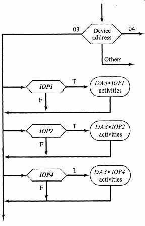
FIG. 3 An asynchronous ASM for IOP signals.
FIG. 3 shows that interface events depend on pseudo-clocks such as DA03-IOP1, formed from a combination of a specific device address and an IOP signal. Bits lR3-IR8 of the LD20's instruction register present a "device address" at all times; spurious device addresses appear as the LD20 processes assorted instructions. FIG. 3 shows that fluctuations of the device address lines produce no algorithmic actions unless they occur while an IOP signal is true.
IOP signals are true only during the execution of IOT instructions. Since the instruction register's outputs change only during the instruction fetch in LD20 state F3, the device address is stable whenever an IOP signal is asserted.
We must also verify that the IOP signals themselves are free of hazards.
IOP signals arise in the LD20 from AND-gate implementations of equations like IOPI = IOPI.EN-lRll Since IOPI.EN and lRll are outputs of flip-flops, their transitions are smooth and free of hazards. Transitions of these two signals are well separated in the ASM; lRll changes only during instruction fetch in state F3, and IOP I.EN changes only at the end of states EO or F1. Therefore, the composite IOPI signal experiences hazard-free F --> T and T --> F transitions. Similarly, IOP2 and IOP4 are free of hazards.
We have shown that the interface pseudo-clocks are free of hazards. We emphasize that in synchronous design we avoid this type of analysis, freeing our minds to construct our algorithm rather than worrying about the behavior of the hardware.
The LD20 will deliver only one IOP signal at a time; we need not worry about two or more of these asynchronous events occurring simultaneously.
Synchronizing Signals to the LD20 and the UART
The LD20 expects replies from its IOP signals to be synchronous with its clock.
How do we achieve this if the LD20's clock is not available to the device interface? We must use the pseudo-clocks developed from the combination of device address and IOP signal, since these are themselves synchronous with the LD20. To satisfy the synchronizing requirement, a selected device must issue proper replies for the duration of the IOP signals. The ASM notation in Fig. 3 is intended to convey this behavior.
To satisfy our LD20 synchronizing requirement, the combinational interface circuits must use only LD20-synchronized inputs to generate the IOSKIP, ACCLR, and ORAC replies. This means that we must synchronize certain DART outputs to the LD20 pseudo-clocks. .
The DART's control inputs DRR (Data Receive Reset) and TBRL (Transmit Buffer Register Load) are both edge-triggered. Any F --> T edge will trigger the DART's actions; the DART has its own internal synchronizing circuitry to avoid difficulties caused by input transitions that are asynchronous to its clock.
We next specify the interface's detailed reactions to each IOP signal.
Algorithm for the Receive Circuit
IOP1 for device address DAD3. To satisfy the PDP-8's protocol, IOSKIP must assume the value of DA03FLG during this event. DA03FLG must become true when a character is available for input, and must become false when the program issues an IOP2 signal. The UART signal DR (Data Received) parallels DA03FLG: it becomes true when a character is ready, and it becomes false when the UART input DRR (Data Received Reset) is asserted. We use a terminal * on names of signals that change independently of the LD20 pseudo-clocks. Thus we have:
DA03FLG* = DR*
DR* (and thus DA03FLG*) may change from F to T at any time, depending on the activities of the terminal and the UART. Before it can serve as a source for IOSKIP, DA03FLG must be synchronized to the LD20's timings. We care if DA03FLG* is synchronized only when IOP1 is true, since only then is the LD20 looking at the signal. To achieve synchronization, we will clock a D flip flop with the hazard-free DA03·l0P1 signal. The flip-flop's input is DA03FLG; the output is DA03FLG.SYNC. IOSKIP must have the value DA03FLG.SYNC for the duration of IOP1. In our ASM, these activities appear as conditional outputs of IOP1:
DA03FLG' -+ DA 03FLG. SYNC IOSKIP= DA03FLG.SYNC
The upward-pointing arrow indicates that the flip-flop activity occurs on the rising (F --> T) edge of the DA03·IOP1 pseudo-clock. The equals sign in the second expression implies that the item on the left has the value of the item on the right for the duration of the pseudo-clock. The synchronizing D flip-flop becomes a part of the interface's architecture.
IOP2 for device address DA03. During this event, we must reset DA03FLG* and must assert the LD20's input signal ACCLR. Clearing DA03FLG* is the PDP-8 programmer's way of clearing the terminal receiver's contribution to the external interrupt signal EXTlNT. Since DA03FLG comes directly from the UART signal DR*, we may clear DA03FLG* by asserting the UART's control input DRR (Data Received Reset). DR*, and thus DA03FLG*, will not return to T until the UART has received another character from the terminal. The ASM conditional output term for IOP2 is ~ ~ IOP4 for device address DA03. During this event (and only during this event), we must place the received data on the LD20's external input lines INPUTO-INPUTll, and assert the PDP-8's input signal ORAC. We gain access to the UART's 8-bit data character by enabling the three-state data outputs RBRS-RBR1, using the control signal RRD (Receive Register Disable). We need to assert RRD. However, we have a small problem with notation. In the ASM charts, signals are considered false except when they are specifically asserted.
Here we have a signal RRD that is normally true, but must be false only when IOP4 is true. We avoid this situation by defining another signal RRE (Receive Register Enable) to use in the ASM chart:
RRE = RRD
During IOP4 time, we assert RRE; it is otherwise false.
The UART provides 8 bits of three-state data for the LD20, but the LD20 expects 12 bits. Our interface must therefore contain 4 bits of three-state zero, which is enabled at the same time as the UART data bits. Adding a three-state zero box to our architecture, we have this ASM for IOP4:
RRE ZERO( ENABLE) ORAC
This completes the algorithm for the receive section of our interface.
Algorithm for the Transmit Circuit IOP1 for device address DA04. During this event, the interface must supply the value of DA04FLG* to IOSKIP. It is tempting to let DA04FLG* be the UART signal TBRE* (Transmit Buffer Register Empty), and for the moment we will make this assumption. Since we must synchronize the signal, we will use a D flip-flop clocked by the DA04·IOPl pseudo-clock. This addition to the architecture has input DA04FLG* and output DA04FLG.SYNC, and our ASM conditional output term is
DA04FLG* --> DA 04FL G. SYNC J
IOSKIP = DA04FLG.SYNC
IOP2 for device address DA04. For this event, the interface's only activity is to clear the output status flag DA04FLG*. Now we have a tricky problem, typical of the kind of irritation found in device interfacing. Using the assumption we made in the previous paragraph, we should clear DA04FLG* by clearing TBRE*, but the only way to clear TBRE* is to load an outgoing character into the UART, using signal TBRL (Transmit Buffer Register Load). The PDP-8's protocol does not allow the loading of a character during IOP2 time, so we must seek an alternative solution.
To hold DA04FLG*, we introduce a flip-flop that we may clear independently of the UART. Now we must determine exactly how to set the DA04FLG* flip flop. DA04FLG* must record the availability of the UART's Transmit Buffer Register (TBR) until the LD20 program clears the flag. Once DA04FLG* is cleared, it must remain false until a new event occurs to make TBR freshly available; we must avoid recording an old buffer availability status. The typical program activity involves testing the flag (IOP1), clearing the flag (IOP2), and writing a character to the interface (IOP4). Once cleared, DA04FLG* should remain false until TBR again becomes available after the transmission of the character. To set DA04FLG*, we must record the occurrence of a F --> T edge of the TBRE* signal. A clock input is the only readily available edge-sensitive element in our design repertoire; TBRE* becomes a pseudo-clock in our ASM, as follows:
This implies a D flip-flop to hold DA04FLG*, as proposed earlier. The flip flop will have T as its input and DA04FLG* as its output. The F --> T transition of TBRE* will act as an active clock edge, which will transfer the true input into the flip-flop, where it will remain until an IOP2 command clears the flag.
After clearing, only a subsequent F --> T transition of TBRE* will clock truth into DA04FLG* again.
The clearing operation originates with the LD20 and is not synchronized with the DART's TBRE* activity. To permit clearing at IOP2 time, we must use a D flip-flop with an asynchronous clear input, such as the 74LS74. FIG. 4 shows this architecture and the controls of the DA04FLG* circuit. The IOP2 conditional output of the ASM chart looks as follows:
( F --> DA04FLG* )
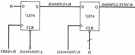
FIG. 4 A circuit for DA04FLG*.
IOP4 for device address DA04. After the tortuous IOP2 exercise, IOP4 is easy! At this time, the LD20 is placing a character on the external output data lines, and our interface must accept it and initiate serial transmission to the terminal. The DART signal TBRL (Transmit Buffer Register Load) will do this if data from the LD20 feeds into the TBR8-TBRl DART inputs. The ASM segment for IOP4 is ( TBRL )
Interrupt Generation
The LD20's external interrupt signal EXTINT* is a composite of the device flag signals. EXTINT* is true if any of the device flags is true. Programmers may clear an interrupt request by resetting the appropriate flag. The terminal interface must transmit the status of its two flags onto the LD20's external interrupt input.
This activity is continuous, independent of the ASM pseudo-clocks. Therefore, the ASM unconditional output for generating an interrupt is I EXT/NT. = DA03FLG. + DA04FLG.
This completes the development of the algorithm for the terminal interface.
FIG. 5 shows the full ASM.
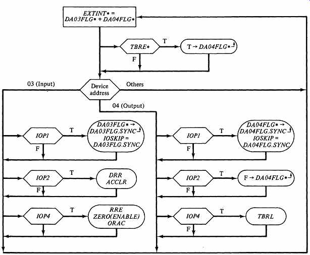
FIG. 5 ASM chart of the interface between an LD20 and a terminal.
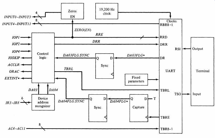
FIG. 6 Architecture of the interface between the LD20 and a terminal.
IMPLEMENTING THE TERMINAL INTERFACE
With the foregoing discussion, specifying the circuit for the interface is simple.
FIG. 6 shows the architecture and a sketch of the control circuits. You should find it straightforward to complete the details of the circuit.
We can provide the clock for the DART's clock inputs with a standard 555 timer circuit, as described in Section 12. The DART is connected with the terminal through a nondigital circuit that matches the TTL-compatible voltage signals of the DART with signal-level requirements of the terminal. The circuit contains a line driver and line receiver such as the 1488 and 1489.
POLISHING THE LD20'S INPUT-OUTPUT PROCESSES
Maintaining the LD20's Control of the Status Inputs
Suppose an LD20 program is trying to read from the terminal. Once the LD20 issues an IOT instruction with a nonzero device address, the algorithm executes states EO, E3, E4, and E5 three times. This occurs whether or not the IOT instruction specifies any IOP signals. For proper hardware execution, we must have valid logic levels (T or F) on the test inputs IOSKIP, ACCLR, and ORAC. This is an important but subtle point: whenever the LD20 executes an IOT instruction, the test signals must be valid. Furthermore, the input signal EXTINT* must be correct at all times.
If we could be sure that the terminal and its interface were attached and operating, our problem would be less serious, since we could require that the device interface respond with false on the status inputs whenever it is not actively responding with truth. But we cannot guarantee that the terminal interface is plugged in whenever an LD20 program issues an IOT instruction. We cannot weasel out of this predicament by rationalizing that no self-respecting computer operator would run a terminal program if the terminal were not turned on. The terminal might be located in another building or another city, outside the control of the operator. In any event, we do not want our hardware to be dependent on an operator's intervention. If the terminal interface were turned off, there would be no logic signals at all on the IOSKIP, ACCLR, ORAC, and EXTINT* lines from the terminal. Obviously, then, the LD20 must protect itself from hardware failures caused by missing control signals.
When will IOT instructions arrive? The LD20 does not know, since IOT instructions are a function of the particular program in the memory. So, we may extend our concept of when the LD20 should protect itself: Whenever its power is on, the LD20 must protect itself against spurious external signals. Since the peripheral power supply is independent of the LD20's power supply, this protection must be in the LD20 hardware itself.
How to do this? Consider gating each input status line with the device address so that the LD20 holds IOSKIP and its counterparts false except when the device is being addressed. This won't work, for three reasons:
(a) Just because the LD20 addresses a device does not assure that the device will respond.
(b) Assertion of the EXTINT* signal occurs independently of device addressing.
(c) Making the LD20 hardware dependent on particular device addresses is abominable design.
We need a soft but constant source of false for the status lines IOSKIP, ACCLR, ORAC, and EXTINT*. By "soft" we mean that any valid true signal will override the LD20's protective false. The solution is to require each peripheral device to transmit its status signals using open-collector outputs. Recall from Section 2 that the open-collector circuit allows and requires a pull-up resistor.
This resistor connects the open-collector output to a source of Vcc, which in the TTL family is equivalent to connecting the output to the high-voltage level.
If the resistor is located in the LD20, then the LD20's power can provide Vcc.
In this way, whenever the LD20 is functioning, the signal it uses will be H unless a peripheral device pulls it to L. By adopting the convention T = L for each of the status signals, we have solved our problem.
This analysis causes us to modify the LD20's design to include pull-up resistors on the inputs IOSKIP, ACCLR, ORAC, and EXTINT*. We also require that peripheral devices provide these signals as open-collector outputs, using the
T = L convention.
The open-collector solution works for our LD20 status inputs even if no peripheral device sends a signal, since the pull-up resistor would hold the input high (false). In Section 12, we describe how to determine a suitable value of the resistor.
Attaching Several Devices
In our design of the LD20, we assume the presence of input-output data and control signals as required by the PDP-8's input-output protocol. We may place these lines into three categories: (a) Signals from the LD20 (device address, IOP, and data out). (b) Data lines to the LD20 (INPUT). (c) Device status responses to the LD20 (IOSKIP, ACCLR, ORAC, and EXTINT*).
Let's investigate how several devices can share these lines. When the LD20 has only one peripheral device, there is little difficulty, since we may attach the interface wires directly to the LD20. When there is more than one device, this crude method fails. Let's examine each of the three categories of signals.
Signals from the L020. All devices share access to the device address, data, and IOP lines. The individual interface must interpret the message on these lines and act appropriately (or refrain from acting). The LD20 must produce output signals of adequate power, but the computer has no further responsibilities for getting signals to their proper destinations.
Data lines to the L020. Input devices must share access to the input data lines. A device must take control at the proper point in its input sequence and at that time must present valid data on each of the 12 lines. At other times, the device must relinquish control. Treating the INPUT lines as a data bus is a convenient way to manage this activity. Of the methods in Section 3 for controlling bus access, the most convenient is to use three-state output controls.
We may formalize the data input system for more than one device by requiring each input device to have three-state control of its data lines to the LD20. Each device must keep its three-state outputs disabled unless an IOT instruction requires the device to place data on the INPUT lines. Since data input is accompanied by the ORAC signal, the LD20 knows exactly when to accept the data.
Device status responses to the LD20. We have already shown that the status input signals will reach the LD20 from open-collector outputs. Since open collector technology provides a wired OR under the T = L convention, peripheral devices should have the open-collector sources of each status signal wired together at the input to the LD20. There are four wired ORs, for IOSKIP, ACCLR, ORAC, and EXTINT*. This method will work well for our LD20 input-output system.
A FINAL WORD ABOUT PART II
The goal of the LD20 project was to extend your design skills using techniques and components at the MSI level of complexity. As a study project in digital design, the hardwired LD20 minicomputer is nearly ideal. This scale of problem is about at the upper limit of practicality for design with hardwired control. The PDP-8 is a simple computer-that is why we chose it for our example. Although the fundamental concepts of register architecture, memory, and sequential control apply to more complex computers as well as to our teaching example, more complex designs require additional components and techniques. More powerful VLSI circuits combining the basic elements of computer control or arithmetic operations are available. In Part III we will describe some of these tools and introduce you to microprogramming-a powerful method of digital control that forms part of the bridge between hardware and software.
The methods and materials of Part II of this book are fundamental components of digital design. With your work thus far, you are well on the way to acquiring a solid proficiency in design.
RESOURCES
ARTWICK, BRUCE A., Microcomputer Interfacing. Prentice-Hall, Englewood Cliffs, N.J., 1980. FLETCHER, WILLIAM I., An Engineering Approach to Digital Design. Prentice-Hall, Englewood Cliffs, N.J., 1980. Asynchronous ASMs.
KUCK, DAVID J., The Structure of Computers and Computations. Vol. 1. John Wiley & Sons, New York, 1978.
PDP8jI and PDP8jL Small Computer Handbook. Digital Equipment Corp., Maynard, Mass., 1972. User's manual for the PDP-81 minicomputer.
PROSSER, FRANKLIN, and ROBERT WEHRMEISTER, C421-C422 Advanced Computer Organization Laboratory Manual. Computer Science Department, Indiana University, Bloomington, Ind. 47405, 1985. Laboratory manual to support the construction, debugging, and study of the LD20 and LD30 versions of the PDP-81. The laboratory project uses the Logic Engine Development System, manufactured by Logic Design, Inc. Ask the authors of this book for information.
WIATROWSKI, CLAUDE A., and CHARLES H. HOUSE, Logic Circuits and Microcomputer Systems. McGraw-Hill Book Co., New York, 1980. Asynchronous ASMs.
QUIZ
1. Describe the asynchronous communication discipline used in terminals and other low-speed serial devices.
2. What type of clocking is necessary in the asynchronous communication discipline? Design Example 4 in Section 6 deals with serial-parallel conversions involving a synchronous stream of data bits. Explain the difference between the two data communication disciplines.
3. Describe the PDP-8's IOT protocol for the terminal, including the expected responses of the terminal interface to the IOP signals.
4. What is the purpose of an input-output interface? Why do we need an interface between the terminal and the LD20? Why does the LD20 not process the terminal's signals directly?
5. Why must the LD20 process the external interrupt signal EXTINT* independently of any IOT instructions?
6. Why must the LD20-terminal interface maintain internal transmit and receive flags?
7. What type of event causes state transitions in an asynchronous ASM? How is this behavior different from a synchronous system?
8. Why must the test inputs in an asynchronous ASM be free of hazards? Explain how we assure that the asynchronous test inputs in the LD20-terminal interface are hazard-free.
9. Describe the behavior of the receive section of the LD20-terminal interface ASM.
10. Describe the behavior of the transmit section of the LD20-terminal interface ASM. Pay particular attention to the circuit in Fig. 4.
11. Describe the behavior of a UART.
12. Why do we not need to present the UART with input signals that are synchronized to its clock?
13. Develop a complete circuit diagram for the LD20-terminal interface suitable for use as a construction guide.
14. Assume that the LD20's system clock is available to the interface. Design a synchronous LD20-terminal interface (using a UART) that is driven by the LD20's clock. Compare this interface with the asynchronous one.
15. The LD20 delivers only one IOP signal at a time. Suppose that the IOP signals for a given device address had no coherent interrelationship; in other words, suppose that they were asynchronous to each other. What effects might this situation have on the proper functioning of the LD20-terminal interface?
16. Expand the LD20-terminal interface to allow its use with other devices similar to a terminal. To do this, add an additional device address to the interface. The new address should allow the LD20 programmer to specify the following DART parameters with suitable IOT instructions: Number of bits per character (from 5 to 8, using a 2-bit code to the DART). Parity mode (odd or even, using 1 DART input bit). Parity inhibit (no parity checking or production, using 1 DART input bit). Number of stop bits (1 or 2, using 1 DART input bit). Also, the new device address should permit the programmer to determine the various error conditions in the DART: Parity error on input (1 DART output bit). Framing error on input (1 DART output bit). Data overrun error on input (1 DART output bit). Design appropriate sequences of IOT instructions to set the DART control parameters and to read the DART status information. Develop an ASM for the interface.
Implement the interface. (You may wish to consult the complete data-sheet description of a DART.)
17. Explain why a computer must maintain hardware control over all incoming status signals. Show how the LD20 handles this problem. Why did we choose an open collector structure? Why not three-state?
18. In the open-collector structure by which the LD20 protects itself against spurious activity of external devices, why do we insist on the convention T = L?
19. Discuss the peripheral device's responsibilities for assuring orderly operation of the LD20's input-output busses when several devices are attached.
Related Articles -- Top of Page -- Home