AMAZON multi-meters discounts AMAZON oscilloscope discounts
The Control Algorithm
The microcomputer manages a variety of operations:
a. Positioning the wire-wrap tool guide, either from information in the wire list or in response to a pushbutton.
b. Processing the panic button signal.
c. Display of data pertinent to a wrap, including the length of the wire and an identification for the wire.
d. Interpretation and execution of operator's commands, such as searching the wire list.
e. Storing the wire list.
With the aid of the software accompanying the display terminal and the peripheral storage device, parts (c), (d), and (e) become routine programming tasks. The organization of the control program is shown in Fig. 6. In response to the operator's commands, the supervisor program selects a subprogram to perform a task, such as seeking the origin or wrapping wires. Upon completion of the task, the subprogram returns to the supervisor, where the controller will await further instructions from the operator.
Part (b), panic-button activity, is best handled by attaching the panic-button signal to the microcomputer's interrupt request line. Asserting the panic signal interrupts the program, causing immediate suspension of its normal activities.
The interrupt subprogram must return control to a standard point in the supervisor program, to await further commands from the operator.
Part (a), moving the stepping motors, requires careful study.
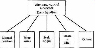
FIG. 6. Organization of the wire-wrap control program.
The wire-wrap algorithm. FIG. 7 shows the software control for wrapping the wires given in the wire list. The footswitch provides the basic sequencing information for this algorithm. Each depression of the footswitch is a "clear to proceed" signal; the algorithm responds by positioning the wrapping tool guide over the next pin. The treatment is similar for the two wraps of a wire; however, prior to beginning each wire, the algorithm provides an opportunity for the operator to intervene. Upon sensing the assertion of the signal from the footswitch, the microcomputer algorithm reads the next record from the wire list and displays appropriate information for the operator's use. The important information to display is the wire length, to allow the operator to select the proper wire, and the wire identification, to permit the operator to know the present point in the wire list.
To process a wrap, the algorithm must use the coordinates of the new pin and the present location of the guide to compute the number of X and Y steps required to reach the next pin. With this information, an X-Y positioning sub program MOVE can direct the stepping of the two motors. The operator will then wrap the first pin.
Prompted by another depression of the footswitch, the algorithm will move the guide to the second pin of the wire and then return to the beginning of the loop to await further instructions. The operator will wrap the second pin and then press the footswitch or enter another command from the keyboard or the terminal.
The MOVE subprogram should move the guide into position over a pin in minimal time. In general, both motors are in motion during each move, but for different durations. Each motor must start slowly and, depending on the distance the beam must travel, may be accelerated to a maximum speed before deceleration.
A motor engaged in a short movement may not reach full speed before deceleration must begin.
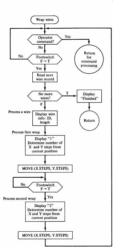
FIG. 7. A software algorithm for wrapping wires in the wire list.
The optimal acceleration and deceleration are complex functions of the stepping speed, but in our application only a conservative approximation is necessary. We may change the stepping speed in discrete jumps , using a constant acceleration factor. FIG. 8 is a typical pattern of software-generated X and Y motor speed changes. The X motor reaches the full speed of 600 steps per second, whereas the Y motor must decelerate before reaching maximum speed.
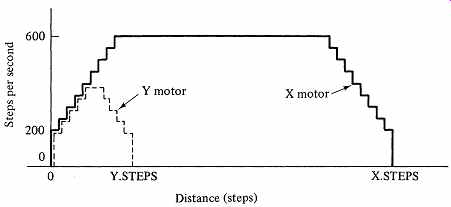
FIG. 8. Acceleration and deceleration patterns of stepping motors.
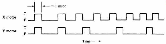
FIG. 9. Typical signal patterns for the independent X and Y stepping
motors.
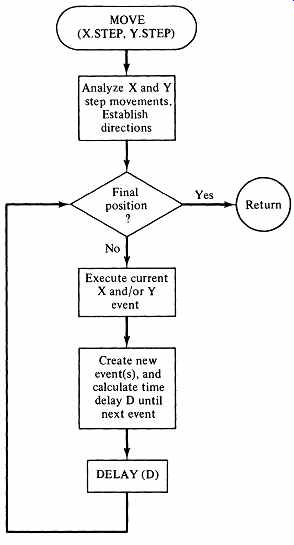
FIG. 10, Flowchart of the sub program MOVE for controlling the simultaneous
movement of the X and Y stepping motors.
Managing the independent motions of the X and Y motors with a single processor requires careful planning of the algorithm. We use a simplified version of the technique of discrete event simulation, which permits a single algorithm to manage several independent sequences of events. In our example, there are two sequences of events: stepping the X motor and stepping the Y motor. The control algorithm must produce the proper sequence of true and false signals for each motor, for instance as shown in Fig. 9.
Managing one motor is relatively simple, requiring only that the algorithm delays the proper time between changes to the motor signals. Given a formula for accelerating and decelerating the motor, the sequence of signals depends only on the distance to be traveled and is completely defined when the stepping subprogram starts. Therefore, when each motor event is processed, the subprogram can determine the time and nature of the next event.
To control both motors, the algorithm keeps track of two intervals: for each motor, the computed time from the present event until the next event.
Upon completing an event, the algorithm delays until the earlier of the two next events arrives, then executes that event and creates a new next event for that motor. This again allows one interval for each motor, allowing the stepping process to advance. The algorithm always processes the earlier event.
FIG. 10 shows the flowchart of the motor-movement subprogram MOVE, the heart of the control. The time-delay subprogram DELAY, called in the main loop of MOVE, accepts a single argument D and pauses for the appropriate interval D before returning. The delays are on the order of milliseconds, whereas the microprocessor's instruction times are on the order of microseconds. Since in this application we do not require exact timings, we may create delays by executing an appropriate number of microprocessor instructions in a loop in the subprogram DELAY. Wrapping Up
This completes our treatment of the controller for the wire-wrap table. We leave as an exercise the development of the algorithm for manual control of the stepping motors. The wire-wrap processes are slow enough that we may perform all the control with microcomputer software. Such control is easier to debug and modify than the hardwired form and allows us to implement more complex designs. In the next example, we describe a system that requires combined hardware and software control.
DESIGN EXAMPLE 2: A TERMINAL MULTIPLEXER-HYBRID HARDWARE-SOFTWARE CONTROL
The device in our second design example is a terminal multiplexer, which will manage the transmission of data between a large number of low-speed computer terminals and a central computer system, merging the information to and from each terminal into a single path in each direction.
This example which arose in a university, represents a common problem in which large numbers of terminals must communicate with a distant point.
One method is to connect each terminal to the computer by a pair of signal paths, one for moving data from the terminal to the computer, and another for moving data in the other direction. Typically, there are separate connections for each terminal. These wires may belong to the organization, or be private lines leased from the telephone company, or be a part of the normal telephone dial-up network.
System designers would like to minimize the overall cost of the communication system; one approach is to minimize the number of long connections to the computer. When only a single terminal exists at a location, there is little one can do except use a set of wires solely for that terminal, or rent a telephone dial-up connection. Where many terminals are close together-in the same room or the same building-there may be an opportunity to save on the cost of separate long communication links with each terminal. This university computing network has a switching system near its main computers. The switching system, purchased from a commercial manufacturer, provides a variety of complex functions to move information among the elements of the network. Among them, it provides access between the computers and individual low-speed terminals.
A more sophisticated service is to handle the high-speed lines over which several terminals communicate. The sharing of the high-speed line among several terminals occurs by time multiplexing the characters: The terminals take turns sending characters over one signal path and take turns receiving characters over another path. Such sharing of high-speed lines is beyond the capabilities of the terminals themselves. We need a terminal multiplexer-a controller such as shown in Fig. 11, located near the terminals, to manage the complex operations involved in the time multiplexing of the data.
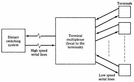
FIG. 11. The environment of the terminal multiplexer.
With the aid of some circuits developed in Section 6, we can construct such a terminal multiplexer, controlled by a microcomputer.
Specifications
Here are the conditions under which the multiplexer must function. We have simplified the specifications somewhat.
Terminal communications. Each terminal communicates at a maximum rate of 300 bits per second in each direction, using the standard asynchronous character communication protocol described in Section 9. Each 8-bit ASCII character requires a total of 10 bits, including the asynchronous protocol's start and stop bits. The transmission is full duplex, since simultaneous communication in both directions is possible. All the terminal communication lines merge into the nearby terminal multiplexer, but so far as a user is concerned, each terminal is independent.
High-speed communications. The terminal multiplexer system is connected to a commercial switching system at a distant site. The transmissions travel over a single full duplex high-speed link, according to the protocols defined by the switching system. The speed of transmission is 9600 bits per second in each direction, although by consulting with the switching system's manufacturer we could raise or lower this value. In normal activity, transmission in each direction is continuous, without a break. The continuous streams of bits consist of 9-bit bytes organized into "frames." A frame begins with a special SYNC byte that marks its start and also permits the identification of byte boundaries in an incoming bit stream. Following the SYNC byte, the frame has one 9-bit byte for each terminal in the configuration. A given terminal's byte always occupies the same relative location in each frame. The byte for a given terminal may contain a terminal data character or, if there is no data character for this time slot, the byte will be a filler, or NULL, byte.
Each 9-bit byte begins with a type specification bit: 0 means that the remaining 8 bits are data, 1 means that the 8 bits are a control code. The control codes are defined by the switching system's manufacturer; the only codes we will consider are SYNC and NULL. FIG. 12 shows the structure of a frame.
This high-speed protocol is an example of synchronous data transmission.
(The terms "synchronous" and "asynchronous" in data communications do not have the same meaning as they do in digital design.) Number of terminals. We may compute the maximum number of terminals as follows: For N terminals, a frame contains N + 1 bytes, or (N + 1) x 9 bits. At 9600 bits per second, a frame requires (N + 1) x 9/9600 sec. The frame contains a spot for each terminal, so each terminal receives processing once in each frame time period.
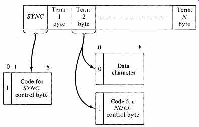
FIG. 12. The frame structure for the terminal multiplexer's high-speed
transmissions.
Each transmission of a character in the asynchronous communication protocol involves 10 bits, of which 8 bits are an ASCII character. At 300 bits per second, each terminal can process at most 30 characters per second in each direction.
Therefore, each terminal requires lo sec to process a character.
Solving for the number of terminals N, we have
(N + 1) x 9 1
9600 30
N= 34
We will use a maximum of 32 terminals in our example; all frames will contain 32 terminal bytes, regardless of the actual number of terminals attached to the multiplexer or turned on.
The Structure of the Terminal Multiplexer
At the terminal side of the multiplexer in Fig. 11, the appearance is of a large number of independent and sporadic transmissions using the asynchronous communication protocol. On the switching system side, the communications are synchronous over a pair of high-speed signal lines, using the specific protocol defined by the switching system manufacturer. Our task is to design something to fit between these two disparate activities. The work of transforming between the synchronous frames and the asynchronous terminal communications will be structured around characters, yet both ends of our system require bit-serial communications, of which the character itself is only a part. We are surely faced with serial-parallel data conversions at each end, to produce the characters that are the common element of each form of communication.
Our choices for dividing the responsibilities are:
a. To translate the high-speed synchronous serial bit stream into 9-bit bytes, and vice versa, using hardware to provide the necessary speed for these operations.
b. To translate serial asynchronous communications from terminals to 8-bit characters (and vice versa), using hardware if possible.
c. To perform the complex manipulations on the resulting characters and bytes using a microcomputer. The hardware in items (a) and (b) will be attached to the microcomputer system bus. We will assume that the data bus is 16 bits wide. FIG. 13 shows the components of the terminal multiplexer.
Let's see how each of these pieces will work.
Switching system communications. In Section 6, we developed serial parallel conversion circuits that support the 9-bit byte format dictated by the switching system's protocol. These circuits include a serial-to-parallel (S ~ P) converter to produce bytes from the serial input line, and a parallel-to-serial (P ~ S) converter to serialize bytes onto the serial output line. The microcomputer is attached to the parallel side of both converters. The rules of operation require the microcomputer to process incoming and outgoing bytes fast enough to keep up with the continuous synchronous serial transmissions. The microcomputer obtains its basic algorithm timing through two status signals from the converters.
A change in the value of READIT prompts the microcomputer to accept a 9-bit byte from the S ~ P converter; a change in FILLIT requires the microcomputer to write a 9-bit byte to the P ~ S converter. The only independent control the microcomputer can exert over the serial bit-stream processing is through the RESET line. Momentarily asserting RESET will cause the S ~ P converter to abandon its normal byte acquisition and search for the special SYNC bit pattern from among the bits of the incoming serial bit stream. This fixes byte acquisition on proper byte boundaries-a necessary operation upon startup, or if the microcomputer loses synchronization with the incoming bytes in a frame, or if there is a break in the serial communications.
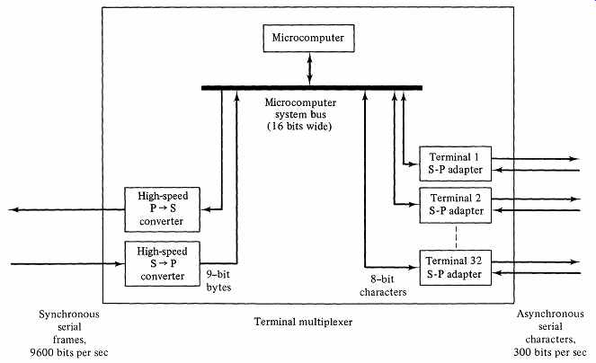
FIG. 13. Components and data flow in the terminal multiplexer.
To attach the serial-parallel converters to the microcomputer system bus, we must give address and data bus assignments to the various device signals.
We will make the following allocations:
Address ADDR.A (read only): READIT FILLIT Data bus bit 10 Data bus bit 9 s ~ P byte buffer Data bus bits 8-0 Address ADDR.B (write-only): RESET Data bus bit 0 Address ADDR.C (write-only): P ~ S byte buffer Data bus bits 8-0
(Read-only and write-only are from the viewpoint of the microprocessor.) In a typical microcomputer memory-mapped input-output bus, the three addresses will each have a 16-bit code; a separated input-output bus will have a smaller code for the device addresses. We must provide our converters with bus interface logic to detect the presence of the three address patterns, and to assert the signals ADDR.A, ADDR.B, and ADDR.C appropriately. The bus interface must deliver the required control signals to the converters to load data from the bus at the proper time.
Since address ADDR.A is read-only (i.e., input to the microcomputer), and addresses ADDR.B and ADDR.C are write-only (output/rom the microcomputer), we do not need bus transceivers. Simple three-state buffers will serve as bus drivers for the elements of ADDR.A. The output-enable signal for this collection of 11 bus drivers is ADDR. AoREAD, where READ is the read signal on the control bus. When the output enable signal is true, the ADDR.A data is available on the system data bus.
Managing ADDR.B and ADDR.C requires a knowledge of the type of elements used in the converter's interfaces with the microcomputer bus. In Section 6, we suggested using a controlled (JK) flip-flop to receive the RESET signal, and a 9-bit enabled D register for the P -? S byte buffer. In order to load these elements under the bus's control, we must generate the correct clock and control signals from the information available on the system bus. The following equations are suitable, where WRITE is the write signal on the control bus:
RESET*.FLIP.FLOP(CLOCK) = WRITE RESET*.FLIP.FLOP(SET) = RESEToADDR.B RESET*.FLIP.FLOP(CLR) = RESET °ADDR.B P-?S.BYTE.BUFFER (CLOCK) = WRITE P-?S.BYTE.BUFFER(ENABLE) = ADDR.B
Terminal communications. You are already acquainted with an LSI device that performs conversions between parallel characters and serial asynchronous bit streams; the DART described in Section 9 does exactly that. We may use a DART for each terminal, and interface each DART to the microcomputer system bus. Various LSI chips perform DART-like functions. For a particular microcomputer, interfacing some chips to the bus is simpler than others. Nevertheless, for all DARTs, there are three vital types of data movement on the bus:
8-bit character data from a terminal into the microcomputer, 8-bit character data from the microcomputer into a terminal, and DART status information for the microcomputer. At the least, the status must include a character-ready signal to describe input from the terminal, and a transmit-buffer-empty signal to control output to the terminal.
We may manage the bus transactions by allocating two microcomputer addresses to each DART, one for data transfer and the other for status. The microcomputer will read a character from a particular terminal by first reading the DART's status, using the assigned bus address for the status port of the selected terminal. If the status indicates that a character is present in the DART, the microcomputer program will read the data portion of the DART. Writing proceeds by a similar sequence of two bus operations: a status read followed, if appropriate, by a data write.
Designing the detailed logic to interface the DART terminal controller with the system bus is not difficult; the pattern is much the same as in the high-speed serial-parallel converters discussed earlier.
The Control Algorithm for the Microcomputer
We have specified the hardware of our terminal multiplexer system: the high speed synchronous serial-parallel converters, the terminal's asynchronous serial parallel converters, and the microcomputer system bus's interfaces to these elements. Let's turn to the master controller for the multiplexer-the micro computer program.
We require our microcomputer to process bytes to and from the high-speed synchronous system at a rate fast enough so that the algorithm never misses its cues. The high-speed serial activities go on all the time, and each frame has a specific position for each terminal. When a terminal's time slot arrives in either an incoming or an outgoing frame, we must process that terminal. It will do us no good to process a terminal at any other time! This important realization shows that the READIT and FILLIT signals are the master timing elements; a change in either of these flags must cause the microcomputer program to process a 9 bit byte. We can forget about the timings of the terminal characters; if we keep track of the position in the frames, we will know when to process each terminal.
The S ~ P and P ~ S bit streams operate independently, so the READIT and FILLIT signals are not synchronized with each other. The microcomputer program should poll (look at) each flag as frequently as it is able, to detect the changes that occur periodically.
How much time is available for processing a byte? Bytes move at the rate of 9600/9 = 1067 bytes per second in each direction. The system must handle 1067 x 2 = 2134 bytes per second, so there is about 470 J,Lsec for each byte.
This corresponds to 100 or more microcomputer instruction executions. Our intuition, borne out by experience, tells us that this is ample time.
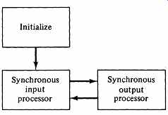
FIG. 14. Algorithm for the terminal multiplexer: basic modules.
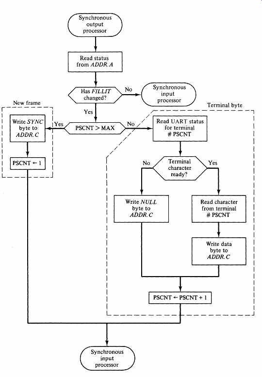
FIG. 15. Algorithm for the terminal multiplexer: synchronous output (P
---... S) processing.
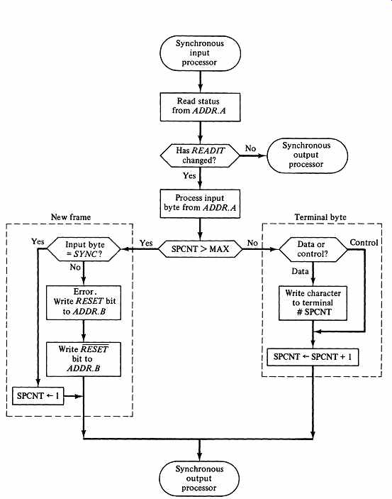
FIG. 16. Algorithm for the terminal multiplexer: synchronous input (S
-> P) processing.
Our initial model of the microcomputer software is in Fig. 14. (Note that this and the following diagrams are software flowcharts, not hardware ASMs.) The initialization occurs only during the startup of the system; thereafter, control flips back and forth between the synchronous input (S ~ P) and the synchronous output (P ~ S) sections, as rapidly as the algorithm can manage.
In each of these two sections of the algorithm, we must poll the appropriate status flag. If we detect no change in the flag, we will go immediately to the other section to perform a similar test on the other flag. If a change occurred in the flag, the algorithm must process a byte before going to the other section.
Consider the synchronous output processor-the software that constructs the bytes of the P ~ S frames. FIG. 15 shows the algorithm for synchronous output. Each time the software detects a change in FILLIT, our program must produce the correct 9-bit byte. To keep track of which byte position in the frame the algorithm is to fill, we use a counter PSCNT whose value ranges from 1 through MAX + 1, where MAX is the maximum number of terminals in the system. In our example, MAX is 32.
Values of PSCNT from 1 to MAX designate the frame slots for each terminal.
When PSCNT exceeds MAX, we have completed a P ~ S frame, so we must transmit a SYNC byte to begin the next frame and reset PSCNT to 1. When PSCNT is in the range of 1 to MAX, we must acquire a character from the designated terminal, if one is available. We then form the 9-bit byte by adding a 0 bit to the front of the character. If the terminal has no new character, we transmit a 9-bit NULL byte, which begins with a 1 bit.
The role of the synchronous input processor is to manage the bytes in the incoming S ~ P frames, dispersing any data characters to appropriate terminals.
FIG. 16 shows the algorithm. If READIT has changed, the meaning of the current byte is governed by a counter SPCNT, similar in function to the PSCNT of the P ~ S algorithm. If SPCNT is greater than MAX, the current input byte must be a SYNC pattern, marking the beginning of a new frame. Not finding a SYNC pattern at this time is a calamity! The only solution is to start S ~ P operations over by issuing RESET to the converter. (Our protocol calls for the microcomputer to follow its assertion of RESET with a clearing of RESET, as shown in Fig. 16.) Once we initiate the reset process, READIT will not change until the S ~ P converter has detected a SYNC byte pattern among the incoming serial bits; therefore, the next byte to appear for processing by the MPU's synchronous input algorithm will be SYNC, to begin a new frame.
When SPCNT has a value of 1 to MAX, the input byte is from a terminal and may contain a data character or be NULL. We transmit data characters to the appropriate terminal through its UART, and ignore null bytes.
FIG. 17 shows the activities of the initialization section of the micro computer algorithm. In addition to other routine activities, initialization sets SPCNT and PSCNT and resets the S ~ P converter system, so that all operations will begin with a new frame.
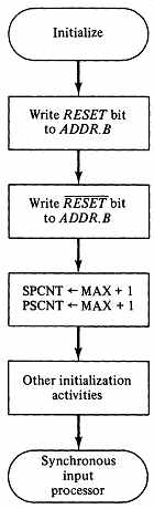
FIG. 17. Algorithm for the terminal multiplexer: initialization.
Checking Out the System
The terminal multiplexer has several hardware components that we were careful to retain as separate modules: the S ~ P and P ~ S converters, the serial bit clock, and the individual terminal controllers. The microcomputer software is also modular, with well-defined sections for processing incoming and outgoing bytes and for initializing the system. All this suggests that we can check out the system in a modular fashion.
The worst approach is to design and construct the system, plug in the parts, hook up the terminals and the high-speed lines, and turn on the power. It is a virtual certainty that the system will not work at this stage, and such an attack may cause considerable damage to valuable components, perhaps even to the switching system or the terminals. In hardware, and in software to a somewhat lesser extent, there is much opportunity for error. Top-down design techniques reduce the likelihood of error in the logical and implementation phases of the project; in Section 12 we discuss some techniques for avoiding trouble in the circuit-fabrication phase. Despite this, it would be unusual for a system to work the first time.
The proper checkout technique would be to test each hardware module separately, using manually produced signals to simulate the inputs that will eventually come from other modules. Here is an advantage of having a manual mode on the circuit clocks. After the hardware module passes this static debugging, we may subject the software modules to similar testing. Here, it may be necessary to use a single-instruction execution mode or to introduce breakpoints into the code. Again, we are trying to do as much debugging as possible under carefully controlled static conditions. Only when the modules pass these tests should you move toward more elaborate testing.
Next, hook two or more of the components together and do more static testing. The extent to which this is feasible depends on the details of the project, but time and effort spent at this level of testing will usually pay big dividends.
When all systems respond satisfactorily, try running the local terminal multiplexer system up to speed. It is still unwise to attach the distance "innocent parties" to your unproven system. Instead, you may wish to consider building into the hardware or software some facilities for providing local loops. These are ways to simulate the effect of the distant communicator (the switching system or a terminal) by generating outgoing data and using this data as incoming data to test the system; we create a local loop to provide some input that would otherwise be difficult to provide during testing. . Next, hook up a terminal and test the system again. One test might be to use a local loop on the high-speed side of the terminal multiplexer, along with a live terminal on the low-speed side. Another stage might be to add a second terminal, to investigate whether the system will perform with more than one device attached. Then, at last, begin tests with the high-speed synchronous lines; this will not only exercise the hardware and software, but will help to determine if your understanding of the high-speed protocol is accurate.
Debugging and checkout methods vary with the individual project, but a systematic, cautious approach is necessary to avoid expensive and time-consuming errors.
Alternative Approaches
Was our separation of the terminal multiplexer problem into software and hardware components a wise choice? Let's investigate some other options. At one extreme, we might have built the whole system in hardware. At the other end, we might have implemented all the control logic in microcomputer software, using minimal hardware.
The algorithms in our example are uncomplicated enough so that a pure hardware solution is feasible. In the actual system on which this example is based, the switching system defines many more frame byte control codes than the SYNC and NULL used here. Although the basic control algorithms remain the same, the full algorithm is heavy with special coding to handle the control sequences. The extra frame byte codes deal with line protocols, terminal connect and disconnect operations, error handling, and other features that make the control algorithm messy with detail. Handling these controls with hardware would be an agonizing chore. The ability to write and correct the control algorithm easily is a major advantage of software control. Microcomputers are fast enough to keep up with the data, using the division of duties in our example, and so we have a strong bias against a pure hardware solution.
Suppose we do everything in software, including the serial-to-parallel and parallel-to-serial conversions. In other words, suppose our microcomputer deals directly with the various serial data streams associated with the terminals and the high-speed lines. Since a computer is a universal logic implementer, it is certainly possible in theory to handle the logic of any algorithm. There are 64 asynchronous bit streams and two high-speed synchronous bit streams to manage in this problem, and we must deal with every bit at just the right time. The software overhead to perform all the necessary chores would be ruinous. The code to interleave the bit processing for all the terminals and the synchronous lines would be very cumbersome. The computer might not be fast enough to do everything required at the proper rate. The effort required to write the software would be considerably greater than the energy expended to produce our hybrid system.
A more modest move toward software would be to use UARTs to reduce the terminal's asynchronous communications to parallel characters, as we did, but also to perform all the high-speed synchronous serial transfers with software.
This approach has some merit, and is probably within the speed limitations of conventional microcomputers, at least for the data rates in our example. However, in developing such a system, we would find numerous places where hardware would be desirable and even necessary, such as in handling the system bus protocols and in deriving the serial bit clock. Furthermore, with a software heavy approach we could not tolerate much increase in the terminal or high speed data rates before the microcomputer is consumed with its duties. The method in our example will permit a considerable increase in the data rates before the system becomes saturated.
CONCLUSION
You have now completed Part III of this book, which concludes our presentation of the art of digital design. In Part I we developed the basic logic operations, circuit drafting methods, and building blocks. In Part II we applied this material to a study of digital design at the fundamental MSI level. In Part III we introduced powerful programming-oriented techniques used in handling many types of complex control problems.
In Parts I and II, we tried to include all the material you need to design at the hardwired level. To avoid distracting you with interesting but less relevant material, we have firmly omitted a number of topics usually found in older or traditional treatments of design.
The introduction to microprogramming and computer-based control in Part III is a foundation for further study. We have presented basic information without covering these subject areas in depth.
Whereas the building blocks available at the hardwired MSI level of design are well established and subject to only minor embellishments, the situation at the LSI and VLSI levels is quite different. New products appear weekly. To maintain excellence and currency as a designer, one must have a sound knowledge of the fundamental principles underlying digital design at all levels. MSI design, feasible and appropriate for complete small systems and for special high-performance systems, is usually not effective for large and complex systems. On the other hand, microprogramming and microcomputer-based control can succeed only when supported by MSI design to provide architectural structures and "glue." In presenting the art of design, we have tried to give you fundamental knowledge that will not be outdated by new technological developments. As you continue to mature as a designer, always remember to seek systematic and fundamental principles and procedures amid the welter of new devices. Happy problem solving!
EXERCISES
1. What is a minicomputer? A microprocessor? A microcomputer? In digital design, does a microcomputer offer support for control, for architecture, or for both?
2. Describe the methodology underlying each of these means of digital control:
(a) Hardwired.
(b) Microprogrammed.
(c) Microcomputer-based.
3. Describe the advantages and disadvantages of each of the methods in Exercise 2.
4. What are the basic components of a microcomputer system? Choose two popular microcomputers and investigate the major components of each. For each system, show how the components are interconnected.
5. Characterize the two forms of microcomputer system bussing methods-memory mapped and separate input-output.
6. Design address detection circuits for the following three device controller addressing configurations: (a) A fixed 16-bit address 2A0016 • (b) A switch-selectable 8-bit address. (c) A 16-bit address with the upper 12 bits fixed at F0016 and the lower 4 bits selectable by switch settings.
7. Describe bidirectional and unidirectional bus interfaces. One often hears of "bi directional data bus" and "unidirectional data bus." Do these phrases have useful meaning? Why or why not?
8. What is a bus driver? A bus transceiver? Using discrete interface components, draw a circuit diagram of a bus interface for a controller with a unidirectional address bus interface and a bidirectional data bus interface.
9. Consult manufacturers' literature and investigate the characteristics of the following LSI chips:
(a) The Intel 8251 Programmable Communications Interface.
(b) The Motorola MC6820 Peripheral Interface Adapter.
10. Two popular microcomputer bus protocols are the VMEBUS and the MULTIBUS II. Locate specifications for these two standards and study their properties.
11. Describe programmed input-output. Choose a large computer, minicomputer, and microprocessor, and determine whether programmed input-output exists. Where it is present, show how it works.
12. You must design a controller for a low-speed (15 bytes per second) paper tape reader, to be used in a microcomputer system with separate input-output. Design at the functional level two controllers for use with the following input-output modes of operation: (a) Programmed input-output without interrupts.
(b) Programmed input-output with interrupts.
13. Describe the interrupt system of two microcomputer systems of your choice.
14. Develop a software flowchart for the manual-positioning event handler in Fig. 6.
15. Develop a software flowchart for the "seek origin" event handler in Fig. 6.
16. For a microprocessor of your choice, implement the algorithm in Fig. 7 for wrapping wires with the wire-wrap table.
17. Discuss the motivation behind the terminal multiplexer project. For the implementation, why did we choose a hybrid hardware-software approach instead of a pure hardware or a pure software solution?
18. In the terminal multiplexer, why is a reset capability necessary for the serial-to parallel converter, but not for the parallel-to-serial?
19. Discuss the effect on the terminal multiplexer hardware and software of:
(a) Increasing the terminal data rate from 300 bits per second to 1200 bits per second, while retaining the synchronous transmission rate of 9600 bits per second.
(b) Increasing the synchronous transmission rate to 100,000 bits per second.
(c) Reducing the maximum number of terminals from 32 to 10.
20. Modify the terminal multiplexer hardware or software (or both) as required to accommodate a frame structure that begins with two SYNC bytes instead of one.
21. Why is the NULL control code a necessary part of the synchronous frame in the terminal multiplexer?
22. In the terminal multiplexer, how does the microprocessor know when to accept a new byte from the synchronous input stream? How does the microprocessor know when to seek a new character from a terminal?
23. Consider the bytes for a particular terminal arriving over the synchronous data line in the terminal multiplexer example. If every byte contains a proper terminal data character, the rate at which characters for this terminal arrive in the system is 9600/(9 x 33) = 32.3 characters per second. Since each character sent to a terminal requires 10 bits in the asynchronous communication protocol, the effective data rate at the terminal is 10 x 32.3 = 323 bits per second-faster than the rated speed of the terminal. To cope with this situation, we must modify the structure of the incoming frame. The switching system at the far end of the 9600 bit-per-second synchronous line must insert a certain number of dummy or "filler" bytes in each frame, preferably just after the SYNC byte or at the end of the frame, to lengthen the frame time.
(a) For the 32-terminal maximum used in the example, calculate the number of dummy bytes required to assure that the data rate to any terminal does not exceed 300 bits per second.
(b) Modify the software to accommodate the new incoming frame structure.
(c) Why is it not necessary to also modify the outgoing frame structure?
24. In the terminal multiplexer example we assumed a microcomputer data bus of 16 bits. Modify the hardware and software to accommodate an 8-bit data bus.
25. Design address detection circuits for the hardware of the terminal multiplexer to accommodate the following:
(a) The Motorola MC6809 system bus.
(b) The Intel 8080 input-output bus.
26. For the terminal multiplexer example, implement the interface between a terminal and a microcomputer of your choice. For example, you might choose the Motorola MC6809 with a MC6850 Asynchronous Communications Interface Adapter.
Related Articles -- Top of Page -- Home