AMAZON multi-meters discounts AMAZON oscilloscope discounts
Objectives
This section will help you understand active devices, how they are used in instrument applications, and the difference between analog and digital circuits.
In this section the following points are discussed.
_ The terms active and passive as applied to electronic components
_ Signal amplification, gain adjustment, and feedback in amplifiers
_ Operation of amplifiers
_ Different types of amplifiers
_ The difference between digital and analog circuits
_ The instrument amplifier
_ Introduction to digital circuits
_ Conversion of analog signals to digital signals
The output from measuring or sensing devices is usually converted into electrical signals, so that they can be transmitted to a remote controller for processing and eventual actuator control or direct actuator control. Consequently, as well as understanding the operation of measuring and sensing devices, it is necessary to understand electricity and electronics as applied to signal amplification, control circuits, and the transmission of electrical signals. Measurable quantities are analog in nature, thus sensor signals are usually analog signals but can sometimes be converted directly into digital signals. Transmission of information over long distances can use analog or digital signals. Because of the higher integrity of digital signals compared to analog signals, and the fact that processors use digital signals, this form of transmission is preferred. Since both forms of transmission are in common use, an understanding of both signal forms is needed and will be discussed.
1. Introduction
Passive components--resistors, capacitors, and inductors--were studied in Sections 2 and 3. This section deals with active components, i.e., devices such as bipolar or metal oxide semiconductor (MOS) transistors, which are active devices and can amplify signals. Collectively all of these devices are referred to as electronics. Transistors are manufactured on semiconductor material (silicon or gallium arsenide) called chips or integrated circuits. Many tens of bipolar or thousands of MOS transistors can be made and interconnected on a single chip to form a complete complex circuit function or system.
2. Analog Circuits
The study of electronic circuits, where the inputs and outputs are continually varying, is known as analog electronics.
2.1 Discrete amplifiers
Transistors can be used to make discrete amplifiers. FIG. 1 shows the circuit of a discrete bipolar (NPN type) and MOS (N channel) amplifier for amplifying ac signals. The difference in the levels of the dc input and output operating points, combined with the temperature drift, requires capacitive isolation between each stage, as well as with the application of direct resistive feedback.
For instance, if the discrete devices were supplied from a 9 V supply, the dc input bias level would be about 3 V, and for symmetry of output the output dc level would be of about 6 V.
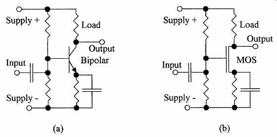
FIG. 1 Circuits of (a) a bipolar discrete amplifier and (b) a MOS discrete
amplifier.
A bipolar device is a current amplifier, and its gain is given by
Gain (b) =?IC (collector I change)/?IB (base I change) (eqn. 1)
A MOS device has a transconductance (transfer admittance) which is the change in the output current for a change in the input voltage. The transconductance is given by
Transconductance (m) =?IS (source I change)/?EG (gate V change) (eqn. 2)
Both b and m, and other device parameters are temperature dependant, so that gain and operating point will vary with temperature.
Example 1-- In FIG. 1b the MOS device has a transfer admittance of 4.5 mA/V. If the load resistance is 5 kOhm, what is the stage gain?
Stage gain = m × 5 kOhm= 4.5 mA/V × 5 kOhm= 22.5
Sensor signals are normally low-level dc signals, which have to be amplified before they can be transmitted to a central control unit, or used to operate indicators or actuators. Discrete amplifiers are not suitable for sensor signal amplification because of their temperature drift and variations in stage gain.
2.2 Operational amplifiers
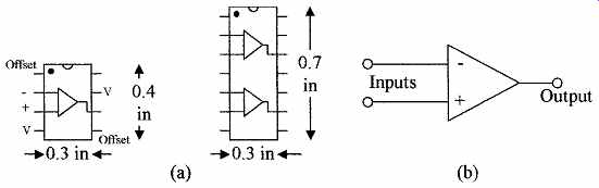
FIG. 2 LM741/107 packages (a) 8-pin and 14-pin DIP showing connections
and (b) Op amp symbol.
The integrated circuit made it possible to interconnect multiple active devices on a single chip to make an operational amplifier (op-amp), such as the LM741/107 general purpose op-amp. These amplifier circuits are small-one, two, or four can be encapsulated in a single plastic dual inline package (DIP) or similar package (see FIG. 2a). All of the discrete devices in an integrated circuit are manufactured as a group, giving all of them similar characteristics, and as they are in close proximity, they are at the same temperature. Thus, the integrated op-amp can be designed to overcome most of the problems encountered in the discrete device amplifier. This is achieved by using pairs of devices to balance each other's characteristics, minimizing temperature drift, and complementary pairs to reestablish dc operating levels. The end result is a general purpose amplifier that has high gain and low dc drift, so that it can amplify dc as well as ac signals. When the inputs are at 0 V, the output voltage is 0 V, or can easily be adjusted to be 0 V with the offset null adjustment. Op-amps require a minimal number of external components. Direct feedback is easy to apply, giving stable gain characteristics and the output of one amplifier can be fed directly into the input of the next amplifier. Op-amps have dual inputs, one of which is a positive input, i.e., the output is in phase with the input; and the other is a negative input, i.e., the output is inverted from the input, so that depending on the input used, these devices can have an inverted or non-inverted output and can amplify differential sensor signals or can be used to cancel electrical noise, which is often the requirement with low-level sensor signals. Op-amps are also available with dual outputs, i.e., both positive and negative going outputs are available. Op-amps are available in both bipolar and MOS technology.
Typical specifications for a general purpose integrated op-amp are:
Voltage gain 200,000
Output impedance 75 ohm
Input impedance bipolar 2 MOhm
Input impedance MOS 10^12
The amplifier characteristics that enter into circuit design are:
Input offset voltage--The voltage that must be applied between the inputs to drive the output voltage to zero.
Input offset current--The input current required to drive the output voltage to zero.
Input bias current--Average of the two input currents required to drive the output voltage to zero.
Slew rate--The rate of rise of the output voltage (V/µs) when a step volt age is applied to the input.
Unity gain frequency -- As the input frequency to an amplifier is increased the gain bandwidth, bandwidth decreases. This is the frequency where the voltage gain is unity.
The schematic representation of an op-amp is shown in FIG. 2b.
The specification and operating characteristics of bipolar operational amplifiers such as the LM 741/107 and MOS general purpose and high-performance op-amps can be found in semiconductor manufactures catalogs.
Many amplifiers use an offset control when amplifying small signals to set the dc output of the amplifier to zero when the dc input is zero. In the case of the LM 741/107 this is achieved by connecting a potentiometer (47 k) between the offset null points and taking the wiper to the negative supply line, as shown in FIG. 3.
In FIG. 4a the op-amp is configured as an inverting voltage amplifier.
Resistors R1 and R2 provide feedback, i.e., some of the output signal is fed back to the input. The large amplification factor in op-amps tends to make some of them unstable and causes a dc drift of the operating point with temperature.
The feedback stabilizes the amplifier, minimizes dc drift, and sets the gain to a known value.
When a voltage input signal is fed into the negative terminal of the op-amp, as in FIG. 4a, the output signal will be inverted. In this configuration for a high gain amplifier, the voltage gain of the stage approximates to (eqn. 3)
The voltage gain of the amplifier can be adjusted with different values of R2 or can be varied by adding a potentiometer in series with R2. When the input signal is fed into the positive terminal the circuit is noninverting; such a con figuration is shown in FIG. 4b. The voltage gain in this case approximates to (eqn. 4)
In this configuration the amplifier gain is 1 plus the resistor ratio, so that the gain does not vary directly with the resistor ratio. This configuration does, however, give a high-input impedance (that of the op-amp) and a low-output impedance.
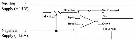
FIG. 3 Offset control for the LM 741/107 op-amp.
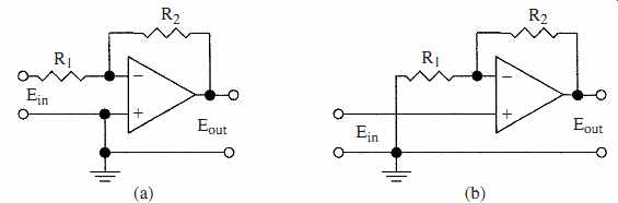
FIG. 4 Circuit diagrams of (a) inverting amplifier and (b) noninverting
amplifier.
Example 2:
If in FIG. 4a, resistor R1 = 1200 ohm and resistor R2 = 150 kOhm, what is the gain, and what is the output voltage amplitude if the ac input voltage is 3.5 mV?
ac output voltage =-3.5 ×125 mV =-437.5 mV =-0.44 V
Example 4.3 In FIG. 4a and b, R1 = 4.7 kOhm and R2 = 120 kOhm.
If a dc voltage of 0.15 V is applied to the inputs of each amplifier, what will be the output voltages? In FIG. 4a
In FIG. 4b
The circuits shown in FIG. 4 were for voltage amplifiers. Op-amps can also be used as current amplifiers, voltage to current and current to voltage converters, and special-purpose amplifiers. In FIG. 5a the op-amp is used as a current-to-voltage converter. When used as a converter, the relation between input and output is called the transfer function m (or ratio). These devices do not have gain as such because of the different input and output units. In FIG. 5a the transfer ratio is given by (eqn. 5)
Example 4 -- In FIG. 5a the input current is 165 µA and the output voltage is -2.9 V.
What is the transfer ratio and the value of R1?
In FIG. 5b the op-amp is used as a voltage-to-current converter. In this case the transfer ratio is given by (eqn. 6)
Note, in this case the units are in mhos (1/ohms), and the resistors are related by the equation
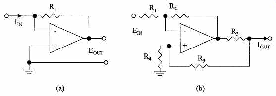
FIG. 5 Examples of (a) a current to voltage converter and (b) a voltage
to current converter.
Example 5 -- In FIG. 5b, R1 = R4 = 5 kOhm and R2 = 100 kOhm. What is the value of R3 and R5 if the op-amp is needed to convert an input voltage of 3 V to an output of 20 mA?

The above circuit configurations can be used for dc as well as ac amplification or conversion, the only difference being that capacitors are normally used in ac amplifiers between stages to prevent any dc offset levels present from affecting the biasing or operating levels of the following op-amps. The dc operating point of an ac amplifier can be set at the input to the stage. High-gain dc amplifiers are directly coupled and use special op-amps that have a low drift with temperature changes. The voltage supplies to the op-amp are regulated to minimize output changes with supply voltage variations.
2.3 Current amplifiers
Devices that amplify currents are referred to as current amplifiers. However, in industrial instrumentation a voltage-to-current converter is sometimes referred to as a current amplifier. FIG. 6a shows a basic current amplifier.
The gain is given by
(eqn. 8)
where the resistors are related by the equation
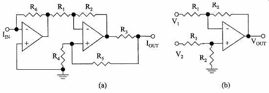
FIG. 6 Circuit diagram of the basic configuration of (a) a current
amplifier and (b) a differential amplifier.
2.4 Differential amplifiers
A differential amplifier is a dual input amplifier that amplifies the difference between two signals, such that the output is the gain multiplied by the magnitude of the difference between the two signals. One signal is fed to the negative input of the op-amp and the other signal is fed to the positive input of the op-amp.
Hence the signals are subtracted before being amplified. FIG. 6b shows a basic differential voltage amplifier. The output voltage is given by (eqn. 10)
Signals can also be subtracted or added in a resistor network prior to amplification.
Example 6 -- In the dc amplifier shown in FIG. 7a, an input of 130 mV is applied to terminal A, and -85 mV is applied to terminal B. What is the output voltage (assume the amplifier was zeroed with 0 V at the inputs)?
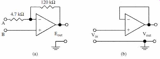
FIG. 7 Schematic diagrams for (a) Example 6 and (b) a buffer amplifier.
2.5 Buffer amplifiers
An impedance matching op-amp is called a buffer amplifier. Such amplifiers have feedback to give unity voltage gain, high input impedance (many mega-ohms), and low output impedance (<20 Ohm), such an amplifier is shown in FIG. 7b. In this context impedance is used to cover both ac impedance and dc resistance.
Circuits have both input and output impedance.
The effect of loading on a circuit can be seen in FIG. 8a. The resistor divider gives an output voltage of 8 V and an output impedance of 2.7 kOhm (effectively this impedance is 4 kOhm in parallel with 8 kOhm). If this divider is loaded with a circuit with an input impedance of 2 kOhm, the output voltage will drop from 8 to 3.43 V. A buffer amplifier can be used as shown in FIG. 8b to match the input impedance of the second circuit to the first circuit, thus giving an output volt age of 8 V across the 2 kOhm load.
Example 7
In FIG. 8b, what is the output voltage of the buffer amplifier? Assume the input impedance of the buffer amplifier is 2 MOhm and its output impedance is 15 ohm.
2 MOhm in parallel with 8 kOhm has an effective resistance of 7.97 kOhm.
From this we get that the buffer loading reduces the output voltage from the resistive divider by 0.01 V, which is about 0.125 percent. The output impedance of the buffer is effectively in series with the 2-kOhm load, so that the output voltage Eout is given by Thus, the total loading effect is a reduction of 0.07 V in 8 V, or about 0.9 percent compared to 57.5 percent with direct loading. This error could be totally corrected if the amplifier had a gain of 1.01.
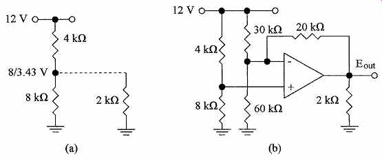
FIG. 8 Circuits shows (a) effect of loading on a voltage divider and
(b) use of buffer in Example 4.7.
2.6 Nonlinear amplifiers
Many sensors have a logarithmic or nonlinear transfer characteristic and such devices require signal linearization. This can be implemented by using amplifiers with nonlinear characteristics. These are achieved by the use of nonlinear elements such as diodes or transistors in the feedback loop. FIG. 9 shows two examples of nonlinear amplifiers using a diode in the feedback loop. In (a) the amplifier is configured as a logarithmic amplifier and in (b) the amplifier is configured as an antilogarithmic amplifier. Combinations of resistors and non linear elements can be chosen to match the characteristics of many sensors for linearization of the output from the sensor.
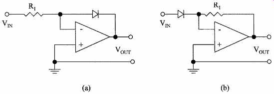
FIG. 9 Circuits of nonlinear amplifiers: (a) log amplifier and (b)
antilog amplifier.
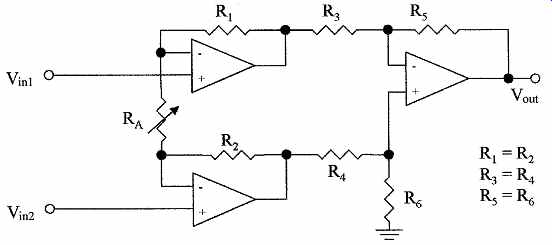
FIG. 10 Circuit schematic of an instrumentation amplifier.
2.7 Instrument amplifier
Because of the very high accuracy requirement in instrumentation, the op amp circuits shown in FIG. 4 are not ideally suited for low-level instrument signal amplification. The op-amp can have different input impedances at the two inputs, the input impedances can be relatively low and tend to load the sensor output, can have different gains at the inverting and noninverting inputs, and common mode noise can be a problem. Op-amps configured for use as an instrument amplifier is shown in FIG. 10. This amplifier has balanced inputs with very high input impedance and good common-mode noise reduction. Gain is set by RA.
The output voltage is given by (eqn. 11)
FIG. 11 shows a practical circuit using an instrumentation amplifier to amplify the output signal from a resistive bridge; R6 is used to adjust for any zero signal offset.
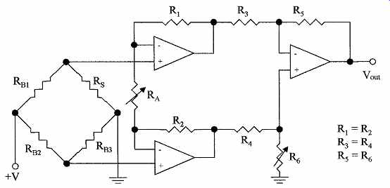
FIG. 11 Instrumentation amplifier used for offset adjustment and to
amplify a signal from a bridge.
2.8 Amplifier applications
In process control, amplifiers are used in many applications other than signal amplification, filtering, and linearization. Some of these applications are as follows:
Capacitance multiplier
Gyrator
Sine wave oscillators
Power supply regulators
Level detection
Sample and hold
Voltage reference
Current mirrors
Voltage-to-frequency converters
Voltage-to-digital converters
Pulse amplitude modulation
More information on the design and use of these circuits can be found in analog electronic textbooks and the like.
3. Digital Circuits
The study of electronic circuits where the inputs and outputs are limited to two fixed or discrete values or logic levels is called digital electronics. Digital technology would take many volumes to do it justice, so in this text we can only scratch the surface. There is a place for both analog and digital circuits in instrumentation. Sensors and instrumentation functions are analog in nature. However, the digital circuits have many advantages over analog circuits. Analog signals are easily converted to digital signals using commercially available analog-to-digital converters (ADC). In new designs, digital circuits will be used wherever possible.
Some of the advantages of digital circuits are
_ Lower power requirements
_ More cost effective
_ Can transmit signals over long distances without loss of accuracy and elimination of noise
_ High-speed signal transmission
_ Memory capability for data storage
_ Controller and alpha numeric display compatible
3.1 Digital signals
Digital signals are either high or low logic levels. Most digital circuits use a 5-V supply. The logic low (binary 0) level is from 0 to 1V, the logic high (binary1) level is from 2 to 5V; 1 to 2V is an undefined region, i.e., any voltage below 1 V is considered a 0 level and any voltage above 2V is considered a 1 level. In circuits where the supply voltage is other than 5 V, a 0 level is still considered as a 0 V level or the output drivers are sinking current, i.e., connecting the output terminal to ground, and a 1 level is close to the supply voltage or the output drivers are sourcing current, i.e., connecting the output terminal to the supply rail.
3.2 Binary numbers
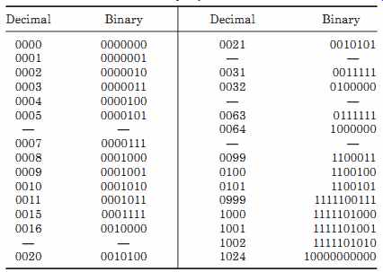
TABLE 1 Decimal and Binary Equivalents
We use the decimal system (base 10) for mathematical functions, whereas electronics uses the binary system (base 2) to perform the same functions. The rules are the same when performing calculations using either of the two numbering systems (to the base 10 or 2). Table 4.1 gives a comparison between counting in the decimal and binary systems. The least significant bit (LSB) or unit number is the right-hand bit. In the decimal system when the unit numbers are used we go to the tens, that is, 9 goes to10, and when the tens are used we go to the hundreds, that is, 99 goes to 100 and so forth. The binary system is the same when the 0 and 1 are used in the LSB position, then we go to the next position and so on, that is, 1 goes to 10,11 goes to 100, and 111 goes to 1000, and so forth. The only difference is that, to represent a number it requires more digits when using a binary system than in the decimal system.
Binary numbers can be easily converted to decimal numbers by using the power value of the binary number. Table 2 gives the power value of binary numbers versus their location from the LSB and their decimal equivalent.
Note that when counting locations, the count starts at 0 and not, as might be expected, at 1.
Each binary digit is called a bit, 4 bits are defined as a nibble, 8 bits form a byte, and 2 bytes or 16 bits are called a word. A word is often broken down into 4 nibbles, where each nibble is represented by a decade number plus letters as shown in Table 4.3. Thus, a word can be represented by 4 decade numbers plus the first six letters of the alphabet. This system is known as the hexadecimal system.
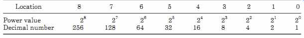
TABLE 2 Power Value of Binary Numbers
Example 8 What is the decimal number equivalent of the binary number 101100101? The equivalent power values are given by
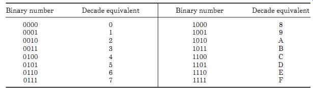
TABLE 3 Numbering Equivalent in the Hexadecimal (H) System
Example 9 -- What is the hexadecimal equivalent of the binary word 1101001110110111? The binary word is broken down into groups of 4 bits (byte) starting from the LSB and going to the most significant bit (MSB).
Binary circuits are synchronized by clock signals which are referenced to very accurate crystal oscillators (< ±0.001 percent), using counters and dividers.
The clock signal can be used to generate very accurate delays and timing signals, compared to RC-generated delays and timing which can have tolerances of > ±10 percent, so that delays and timing will be done almost entirely by dig ital circuits in new equipment.
3.3 Logic circuits
The basic building blocks in digital circuits are called gates. These are buffer, inverter, AND, NAND, OR, NOR, XOR, and XNOR. These basic blocks are inter connected to build functional blocks such as encoders, decoders, adders, counters, registers, multiplexers, de-multiplexers, memories, and the like. The functional blocks are then interconnected to make systems, i.e., calculators, computers, microprocessors, clocks, function generators, transmitters, receivers, digital instruments, ADC and digital-to-analog converters (DAC), telephone systems and the like, to name a few.
FIG. 12a shows the circuit of a complementary MOS (CMOS) inverter. The circuit uses both N- and P-channel complementary devices (note device symbols).
FIG. 12b shows the equivalent gate symbol. When the input to the gate is low (0) the positive-channel MOS (PMOS) is "ON" and the negative MOS (NMOS) is "OFF" so that the output is held high (1), and when the input is high (1) the PMOS is "OFF" and the NMOS is "ON", which will hold the output low (0), so that the input sign is inverted at the output. One of the MOS devices is always "OFF", so that the circuit draws no current from the supply (except during switching) making CMOS circuits very power efficient.
3.4 Analog-to-digital conversion
The amplitude of an analog signal can be represented by a digital number, for instance, an 8-bit word can represent numbers up to 255, so that it can represent an analog voltage or current with an accuracy of 1 in 255 (assuming the con version is accurate to 1 bit) or 0.4 percent accuracy. Similarly a 10 and 12-bit word can represent analog signals to accuracies of 0.1 and 0.025 percent, respectively.
Commercial integrated A/D converters are readily available for instrumentation applications. Several techniques are used for the conversion of analog signals-to digital signals. These are Flash converters which are very fast and expensive with limited accuracy, that is, 6-bit output with a conversion time of 33 ns. The device can sample an analog voltage 30 million times per second.
Successive approximation is a high-speed, medium-cost technique with good accuracy, that is, the most expensive device can convert an analog voltage to 12 bits in 20 µs, and a less expensive device can convert an analog signal to 8 bits in 30 µs.
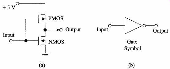
FIG. 12 Circuit components used to make (a) a MOS inverter and (b)
an inverter symbol.
Resistor ladder networks are used in low-speed, medium-cost converters. They have a 12-bit conversion time of about 5 ms.
Dual slope converters are low-cost, low-speed devices but have good accuracy and are very tolerant of high noise levels in the analog signal. A 12-bit con version takes about 20 ms.
Analog signals are constantly changing, so that for a converter to make a measurement, a sample-and-hold technique is used to capture the voltage level at a specific instant in time. Such a circuit is shown in FIG. 13a, with the wave forms shown in FIG. 13b. The N-channel field effect transistor (FET) in the sample-and-hold circuit has a low impedance when turned "ON" and a very high impedance when turned "OFF". The voltage across capacitor C follows the input analog voltage when the FET is "ON" and holds the dc level of the analog volt age when the FET is turned "OFF". During the "OFF" period the ADC measures the dc level of the analog voltage and converts it into a digital signal. As the sampling frequency of the ADC is much higher than the frequency of the analog signal, the varying amplitude of the analog signal can be represented in a dig ital format during each sample period and stored in memory. The analog signal can be regenerated from the digital signal using a DAC. FIG. 14a shows the block diagram of the ADC 0804, a commercial 8-bit ADC. The analog input is converted to a byte of digital information every few milliseconds.
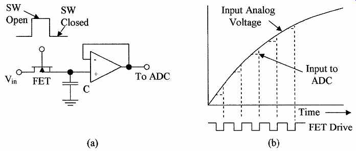
FIG. 13 (a) Sample and hold circuit and (b) waveforms for the circuit.
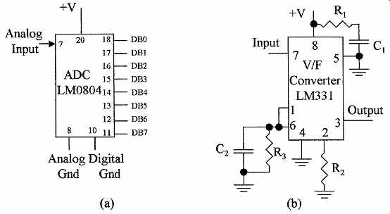
FIG. 14 Different types of converters: (a) LM 0804 ADC and (b) LM 331
V/F converter.
An alternative to the ADC is the voltage-to-frequency converter. In this case the analog voltage is converted to a frequency. Commercial units such as the LM 331 shown in FIG. 14b are available for this conversion. These devices have a linear relation between voltage and frequency. The operating characteristics of the devices are given in the manufacturers' data sheets.
4. Circuit Considerations
Analog circuits can use either bipolar or MOS-integrated amplifiers. Bipolar op-amps tend to have a lower input dc offset, but MOS op-amps have higher input impedance. Since a large number of op-amps and special amplifiers are available, the manufacturers' data sheets should be consulted to decide which amplifier is best suited for a specific application.
Digital circuits can be divided by the number of components integrated onto a single silicon chip into small-scale, medium-scale, and large-scale integration.
In small-scale integration (up to 100 devices) such as the SN 54/74 family of dig ital circuits, both bipolar and CMOS devices are used. This family of devices contains gates and small building blocks. Medium scale integration (over 100,000 devices) will use only CMOS devices. This is because of the excessive power requirements, high dissipation, and relatively large size of bipolar devices. Such circuits contain large building blocks on a single chip. Large-scale integrated circuits contain over 1,000,000 devices, and use CMOS technology. These devices are used for large memories, microprocessors, and microcontrollers, and such circuits can contain several million devices.
Systems containing a large number of gates are now using programmable logic arrays (PLA) to replace the SN 54/74 gate family of devices, as one of these devices can replace many gate devices, requires less power, and can be configured (programmed) by the end user to perform all the required system functions.
Summary
In this section, op-amps, their use in amplifying analog signals, and their use as signal converters were discussed. The relation between analog signals and digital signals, and the conversion of analog-to-digital signals was covered.
Salient points discussed in this section are:
1. Discrete amplifiers, their use in ac signal amplification, and why they are not suitable for dc signal amplification
2. The op-amp and its basic characteristics, its versatility and use in signal amplification, and methods of setting the zero operating point
3. Signal inversion and non-inversion, methods of applying feedback for gain control and stability
4. Use of the op-amp as a signal converter, impedance matching, set zero control, and span adjustment
5. Configuration of op-amps to make an instrument amplifier for accurate signal amplification and noise reduction
6. Introduction to digital circuits plus a comparison between analog and digital circuits
7. Binary, hexadecimal, decimal equivalents, and conversions between the counting schemes
8. Logic circuits used in digital systems and circuit considerations
9. Conversion of analog signals to digital signals and the resolution obtained
Problems:
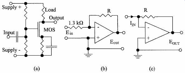
FIG. 15 Circuits for use in (a) Probs. 2 and 3, (b) Probs. 4,
5, and 6, and (c) Probs. 8 and 9.
1. What is the difference between analog and digital circuits?
2. What is the stage gain of the discrete amplifier shown in FIG. 15a if the MOS device has an admittance of 5.8 mA/V and the load resistance is 8.2 kOhm? Assume the capacitors have zero impedance.
3. What load must be used in the discrete amplifier shown in FIG. 15a if a stage gain of 33 is required? Assume the capacitors have zero impedance.
4. What is the stage gain of the op-amp shown in FIG. 15b if R = 285 k??
5. What is the value of the feedback resistor needed for the op-amp shown in FIG. 14b to obtain a voltage gain of 533?
6. Redraw the inverting amplifier in FIG. 15b as a noninverting amplifier with a voltage gain of 470.
7. What is the offset null in an op-amp used for?
8. If the amplitude of the input in the amplifier shown in FIG. 15c is 14 µA. What is the amplitude of the output if the feedback resistor R = 56 k??
9. What is the transfer ratio of the amplifier shown in FIG. 15c, if the feedback resistor R = 27 k?
10. What is the output current if the input voltage is 3.8 mV in FIG. 16a? Assume R3 = 1.5 k.
11. What is the value of R3 in FIG. 16a for a transfer ratio of 8.5 mA/µV? Assume R2 = 100 kOhm
12. If in FIG. 16b, input A is 17 mV, and input B is -21 mV, what is the value of the output voltage if R = 83 kOhm
13. What is the base number used in a binary circuit?
14. What is the decimal equivalent of 1011001?
15. What is the binary equivalent of 0037?
16. What is the hexadecimal equivalent of 011010011100?
17. What is the hexadecimal equivalent of 111000111010?
18. How many bits are there in a (a) byte and (b) word?
19. Does a "1" level represent an output that is sourcing or sinking current?
20. Name the types of gates used in digital circuits.
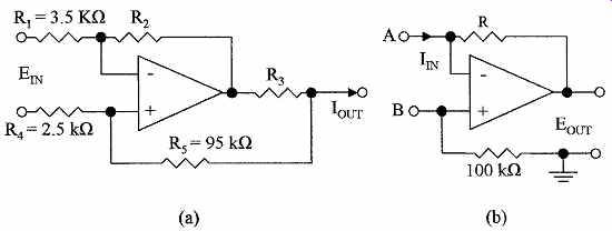
FIG. 16 Circuits for use in (a) Prob. 10 and 11 and (b) Prob. 12.
Related Articles -- Top of Page -- Home