BY WILLIAM CHATER
ABOUT THE AUTHOR: William Chater has a BS in electrical engineering (Cornell 49) and has worked in the nuclear instrumentation field, and more recently with scientific instrument space science experimental payload design. As well as constructing loudspeaker and hi-fi projects. Mr. Chater is also an amateur violin player and builder.
ANY OF THE PREAMPLIFIERS listed in Audio's 1989 Audio Equipment Directory (October Issue) offer the latest in low noise, high overload level, multiple tape and processor loops, and marvelous flatness of response and low distortion. But for a DIY preamplifier builder, some less common features can add a great deal to the quality of a sound system. Because it is possible to build this sort of improvement into your sys tem in a handmade instrument, it is very interesting to see what can be done to justify such an investment of time and skill.
I have listed here a few properties which may add significantly to the over all sound quality of a system, and which may or may not be found in commercial equipment:
RIAA stage gain adjustability, so you can tailor the gain or overload levels of the system to a particular phono RIAA input capacitance adjustability, to provide tailoring of the capacitance to a certain cartridge; a phase-reversing switch lets you experiment with the effects of phase in each channel and correct for those signal sources which you might have recorded 'out of phase''; a gain-switchable section, allowing for + 6dB of adjustment to permit tailoring system gain to the sensitivity of your power amplifier and speakers;
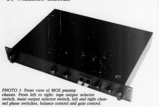
PHOTO 1: Front view of MOS preamp chassis. From left to right: tape output selector switch, main output selector switch, left and right channel phase switches, balance control and gain control.
* a line driver capable of flat response up to the limits of the speakers, with the ability to drive long high-capacitance signal lines and low impedance loads, so you can locate the power amplifier at a distance from the control center; a tape driver capable of high current output, similar to the line driver, and a noise- and click-free turn-on and turn-off performance.
To create a preamp having these features, I was drawn to the design to be described. I also wanted to follow the lines of the MOS power amplifier ("A 40W MOSFET Power Amplifier," TAA 2/88) with a family resemblance in sound and style, and to explore the ad vantages for audio to be found in what is still a new element, the MOS transistor.
Minimalist Approach
To build a preamplifier with these features, but with a simple and straightforward signal flow, I decided not to include tone functions, frequency limit filters or other processing stages. These functions can be introduced via the tape loop connections and thus can be built within a separate system component. This minimalist preamp function line-up becomes an RIAA stage, a tape line driver, and a main output line driver for each channel. These, with the necessary inputs, switching, and level and balance controls then become the essence of the control center.
The signal flow path is pretty well dictated by the standards of the industry.
Signal gain from an active circuit is required to bring the phono level up to that of the FM, CD and other line level inputs. Switching should be done at a relatively high level, and the gain adjustment planned must follow that. At the output, we must drive the envisioned long lines. The resulting block diagram of the preamp is shown in Fig. 1.
The line driver provides the phase inverting/non-inverting selection and the variable gain. Thus, much of the complexity of the design falls into this one block. I will describe the effects of these choices in a following section on the line driver.
I chose a separate selector switch for routing the signal to the tape outputs so the preamp can be used to monitor one signal while taping another. This topology also allows copying from tape
------------- Passive RIAA Network Design
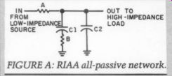
Figure A shows a network of passive components which will produce the RIAA frequency curve. We recall that the ''corner'' frequencies of the RIAA characteristic are at 50, 500 and 2,122Hz. A rolloff corner (''pole'') occurs at 50 and 2,122Hz, while a transition from a 6dB/octave downward slope to flat response (a ''zero'') occurs at 500Hz, according to the standard.
It is not as simple as it might appear to insert these frequency standards into the response formula of the net work and: then derive from this the values of the two capacitors and two resistors. Many small cross-product terms arise in the solution which make the complete solution very tedious. It is easier to proceed in the following manner.
The algebraic solution of ''gain'' for the network is:
1) Vour/Vpy = (1+sBC1)/{1 + s(BC1+AC1+AC2) + s? ABC1C2]
… where s is the frequency variable (jw).
This relation unfortunately is not factorable into two poles of the form (1 + sR1C1})(1 + sR2C2) because the cross-product terms in the denominator are all too much alike in magnitude. Otherwise the factored result might permit us to assign the values of R1C1 and R2C2 separately and a solution would result.
Instead, we use a denominator in the ideal form just given, in which we know the desired pole locations are at 50 and 2,122Hz, that is:
R11C1 = 1/(2x*50) = 3,183 uS R2C2 = 75uS
This forms a denominator (by multiplying it out):
(1 + s(RIC1 + R2C2) + $2(RIR2C1C2)) … for which the s term is known to be 3,183 + 75 = 3,258uS and the s squared term is the product 238.7E-9 To produce an identical response to this standard with our network, we let these s and s**2 terms be equal:
2) BCl1 + AC1 + AC2 = 3,258uS
3) ABCIC2 = 238.7E-9
This is only two equations with four unknowns, but we are at liberty to choose the impedance level of the circuit by selecting one part first. Let us (with malice aforethought) set C1 equal to 0.288uF. This rather uneven number is actually easy to buy, being the parallel of the two standard values 0.22 uF plus 0.068 uF. Setting C1 lets us solve for the rest of the circuit if we can know one other relation. That relation is obtained from the zero in the numerator. Fortunately, the numerator is a simple corner frequency known to be at 500Hz:
BC1 = 1/(2#x*500) = 318.3uS
We immediately know from this result that B = 1,1050.
Using this, we can manipulate the relations 2) and 3) by straightforward algebraic operations to result in:
A[C1+C2) = 3,258 - 318.3 = 2,939.7uS
AC2 = (238.7E-9}/BC1 = 750 uS
Thus, AC1 = 2,939.7 - 750 = 2,189.7uS
A = (2,189.7E-6)/C1 = 7,603 ohm
C2 = (750 E-6)/A = 0.0986 uF
An entirely satisfactory set of ''real life'' part values is thus:
A = 7500
C1 1100
C2
0.288uF
0.10 uF
which will produce results within 0.2dB of the standard. We can obtain a closer fit with a little experimenting and value selection. The 7,500-ohm value for resistor A allows for a little source resistance to drift the result toward a closer fit to the curve.
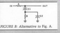
FIGURE B: Alternative to Fig. A.
Another form of the network is that of Fig. B, which moves the shunt capacitor to a position across resistor B.
The equation for this network is a little different:
s(BC1+BC2+AC1) + (s**2)(ABC1C2)]
Using the same approach to this net work results in the solution, with the 'chosen' part being resistor A = 10k this time:
A = 10k
B = 8060
C1 = 0.294uF
C2= 0.1uF
… where the value of C1 can be made up of 0.27uF and 0.022uF, for instance, with the other values being standard part values.
An experimental circuit with the first of the above networks has been made up and tested against the Old Colony KL-3 Inverse RIAA network, with errors of 0.1dB maximum at any frequency in the range up to 20kHz.
I have not tried the second network, but it is likely the results would be just as good.
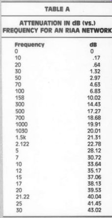
The calculated results of the first network given above are listed in Table A.
TABLE A
ATTENUATION IN dB (vs.) FREQUENCY FOR AN RIAA NETWORK
The salient checkpoints are at 0, where the gain is unity; at 50Hz, where the loss is 3dB; at 500, where the loss would be 17dB but for the slight effect of the roll-off at 75 uS; at 1,030, where the loss is 20dB; at 2,122, where the loss would be 3dB below the "midband" level but for the slight effect from the lower-frequency "zero" at 500Hz, and at 21.22kHz, where the loss is 40dB.
These values are the ones predicted by the network values given in the preceding text, and might vary slightly from the RIAA standard in its published form.
-----------------
... 1 to tape 2 while monitoring either tape, or listening to some other pro gram source.
The RIAA Stage The RIAA stage is a preamplifier's most demanding circuit design task. It must address the noise problem. At the same time, it must provide ample dynamic headroom for the phono cartridge signal, i.e., the circuit must be able to handle a worst-case transient amplitude without being driven into nonlinearity.
This requirement means the input amplifier may be called on to handle the highest signal amplitudes in the pre amp signal chain.
The RIAA stage must provide the correct frequency contouring. The simplest way of providing this is a one-loop RC feedback network around a gain stage.
Many authors have observed that this connection puts a large current demand on the output at high frequencies, since the gain must be reduced to the least amount at the high frequency end of the contour (see "The Borbely Pre amp," by Erno Borbely, TAA 4/85).
To avoid this current demand, we can use a passive RC network to pro vide the high-end rolloff. This leaves just the two lower frequency corners of the contour to be provided by the active feedback loop. It is, of course, possible either to put the low frequency tailoring first or to reverse this arrangement by providing a flat gain stage driving the high-end RC rolloff, followed by the low frequency amplifier loop.
A flat gain amplifier stage driving a wholly passive RC network designed to provide all the RIAA shaping in one net work is also available to the designer.
Some listeners, it seems, are able to hear the difference between these various connections, and some are much in favor of the wholly-passive method (see sidebar ''Passive RIAA Network Design").
I have designed the preamplifier with a choice of two of these styles. By leading off with an active-feedback low noise amplifier loop having the low frequency comers in the feedback loop, a completion of the RIAA curve is then supplied by a subsequent RC at a relatively low impedance level. In this way, the one active amplifier provides the whole RIAA curve.
For a second choice, it is then possible to alter this amplifiers feedback loop components so as to provide flat gain with frequency. You can then connect a passive RIAA network to the out put of this gain stage, thus converting the circuit to the wholly passive version. A flat gain post-amp of about 16dB is needed following the network to recover the signal to the desired level.
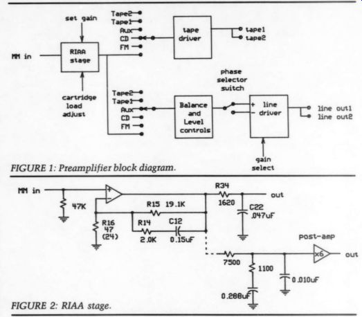
FIGURE 2: RIAA stage.
Figure 2 shows feedback parts R14, R15 and C12 to develop the 50 and post-amp 500Hz corners of the RIAA curve. R34 and C22 add the 75uS high-frequency rolloff part of the RIAA curve. The gain at kHz is set by resistor R16 to bring a 5mV moving magnet (MM) cartridge signal up to a level of 200mV. This amount of gain sets the 1kHz overload figure at 250mV, which is well above ...
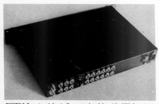
PHOTO 2: Rear view of chassis. Connectors from left to right: MM phono inputs, FM tuner inputs, CD player inputs, Aux. signal inputs, 3-position gain set switch,
tape 1 and 2 inputs, tape 1 and 2 outputs, line outputs (duplicated). Far right- power input jack, power switch, fuse.
the limits of the MM cartridges listed in Audio's Equipment Directory.
The use of a less sensitive cartridge can be accommodated by selecting the lower value of R16 which raises the whole curve by 6dB. The optional post amplifier need only be added if you want to convert the circuit to all-passive. The output signal is not required to drive anything but the 100k level and balance controls, so the post-amp can be designed to have minimum complexity.
Input Transistors With the idea of endowing the preamp with a low-noise input stage, we arrive at a design choice: what to use for the active elements? As mentioned before, there is an urge to experiment with MOS units. Regrettably, the ''low noise'' MOSFET transistors available are made for low-noise RF amplifier ser vice, not for DC and audio frequency service as we require here. I have there fore experimented with many of the JFET units available and have found (as have others before me) that the best presently available seems to be the Toshiba 2SK147 JFET.
This unit, although not expensive, is quite difficult to obtain so I searched for an alternative and found a ''low-noise"' replacement JFET, the widely available n-channel NTE458. This unit has a gain factor (gm) of about 15,000 micromhos at a drain current of 5 mA, and although it is not as low noise as the Toshiba unit, it is an acceptable substitute. The NTEA458 current-drain voltage characteristic is shown in Fig. 3. To get an idea of the spread of gain to be found in this device, I show a group of 10 of these devices' drain current versus gate bias curves in Fig. 4. They seem quite uniform. In particular, the slopes (gm) of the curves are very much alike at a chosen drain current, even if the gate to source bias voltage is different.
I considered the construction of the RIAA input stage with the now well accepted differential-complementary in put arrangement. This circuit provides the advantages of low distortion and compatibility with balanced circuitry of the following amplifier stages. It also offers an enhancement of the noise performance by paralleling the active input transistors, which results in a 3dB noise reduction if the n and p transistors are of equal noise level. In spite of these ad vantages, I chose the simpler single

FIGURE 3: NTE458 n-channel junction FET. FIGURE 4: Ten NTE458 JFETs. FIGURE 5: A noise model. The square root of the sum of noise voltages is 1.36uV, which is 71dB (unweighted) below a nominal 5mV input signal.
... differential pair because of the difficulty in finding such n-p matched characteristics.
Consider the noise signal equivalent circuit of an RIAA differential input stage as in Fig. 5. The noise level is com posed of the contributions of these various sources. The main sources are the all important input transistor, the various resistors and the noise level associated with the phono cartridge itself. All these resistors generate noise voltages across themselves as determined by the temperature and the bandwidth:
Ey RMS = (4KTBR)**1/2
By using the known value of Boltzman's constant, K = 1.38 E-23 joules per degree Kelvin, and using a room temperature of 300° K, we get:
Ex RMS = (2.23E-8)*(R**1/2) for an audio bandwidth of 30kHz.
The various resistors in Fig. 5 have been labeled, each with its open circuit terminal noise voltage. These noise sources combine as the square root of their summed squares. The resulting noise output of the circuit of Fig. 5 is mainly set by the values from the pick up, the transistors, and the resistors R07, 08 and 16. The contribution from resistor R02 is quite small.
We notice from this analysis that the noise contribution from the pickup resistance is not negligible. It is enough,
------------
Some Amplifier Device Properties
Suvi ths his plifier devices described in the text, I first generated the anode current ver wk merit bles conve fa wicks Syl
These data were posed automatically a plotter station curve plotter, ex ol for the tube, which data were already available in the tube manual.
The results of these plots are given in Fig. 1. The tube data are for two sections in parallel, to bring the tube into the same current range as the other devices. The devices appear to be quite judgment.
we see a little further into this? The next step is to normalize the curves so they all extend over the same voltage range. We can do this by dividing each curve's horizontal voltage value by its own value at the high end of the range.
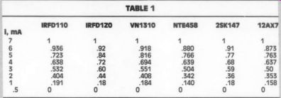
I used the point at i = 7mA for this normalizing point, so I could use an intermediate current like 4mA as an operating point. This result is given in Table 1.
Now let's hope we are being totally fair to all six devices: they cross at two points and yet retain their individual curvatures between these points. The device which registers the straightest at the chosen operating point will now be the one that, all other things being equal, will produce the lowest harmonic output and thus be the favored one, if any.
A first look at Table 1 shows that they differ. How shall their ''straight ness'' best be shown? A standard measure of a curve's is the mathematically defined ''curvature,"' which is given by the formula:
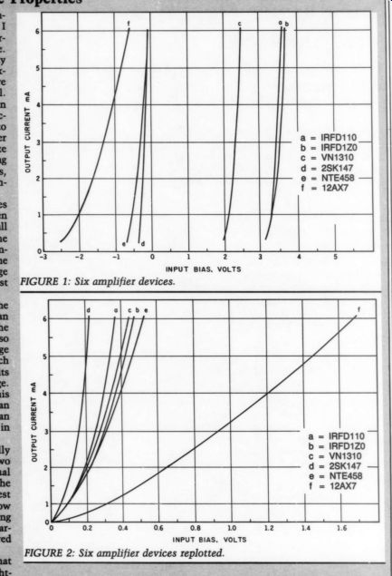
FIGURE 1: Six amplifier devices.
FIGURE 2: Six amplifier devices re-plotted.
1) K =d2/(1 + (d1)**2)**3/2 where d1 is the first derivative of the function, and d2 is the second derivative at the selected operating point.
Now, to get a value for these derivatives, we can fit a power relation to the data. I used the formula:
---------------------
--------------------
ness'' parameters of six amplifier devices. The value R is the radius of curvature; the larger the radius, the straighter the relation. R is given in dB above the smallest value of the six in each case. For the meaning of the K value from which R is obtained, see text.
The results of this show some interesting things. First, the tube comes out near the top in straightness. This ...
TABLE 1
------------------
We can get a and b from the values in Table 1 in a variety of ways. In one way we can use a computer if we have one running such a program or we could use a hand calculator such as the HP11C running a linear-regression least-squares fit routine. A third possibility is to fit a straight line by eye to the plot on log-log paper of relation 2). We could do this by using the log of 2): In(i/a) = b Inv, for which a plot of In (i/a) versus In V will have the slope b.
I have used both the plot method and the hand-calculator methods to develop the results of Table 2.
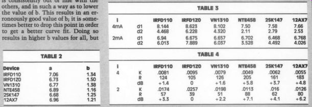
The constants a are not all equal to 7mA because the least-squares curve fitting routine adjusts for a minimum error by slightly varying this parameter. The b parameter is an indication of the amount of bending.
One feature we often see in the above plot method is that the lowest datum point (0.5mA in the case given) is consistently out of line with the others, and in such a way as to lower the value of b. This results in an erroneously good value of b; it is some times better to drop this point in order to get a better curve fit. Doing so results in higher b values for all, but
TABLE 2
their relative ranking is usually the same.
To introduce our derived a and b values to the curvature relation, we need the missing derivatives in numerical form. They are:
dl = abv**b-1) d2 =ab(b-1) v**(b-2)
These values are tabulated at the operating point of v {which is different for each device) corresponding to current values of 2 and 4mA in Table 3.
We can now, at last, use these values to get a table of curvature numbers according to the relation 1) given before. Also included is the reciprocal of the curvature, R, which is called the radius of curvature. I prefer to use this radius, because it is a number which is larger for the better ''straighter'' device. We can render it in dB, as Table 4, using the lowest R value for a base 0dB.
Table 4 is a listing of the ''straight result may not surprise many; tubes are enjoying a revival for audio. An other interesting feature is the high ranking of the JFET NTE458. In all of the studies made in this survey, this device has consistently placed at or near the top. Further, the MOS units are quite similar, with the 1310 and the 110 units a little better than the 1Z0 at higher bias currents, but not at lower ones, such as at 1mA. (I have values for this bias, but they are not given here.) This may not be surprising, as the 1310 and 110 units are higher current devices anyway.
The tube drops down the scale of straightness at low currents, as would be expected from a look at the tube manual. The junction transistors usually seem a little better than the MOS units, and the 458 often exceeds the tube. These results all are spread over a rather small range, however, and may merely show that the actual curvatures of all six devices (as in Fig. 2) are not as different as it might have appeared.
TABLE 3
------------------------
… in fact, to make the difference between the 25K 147 and our replacement device a relatively moderate difference. Thus, the reason for using a 2SK147 would not be simply the lower noise level so much as its lower incidence of ''popcorn'' noise. Adding up the effects of the noise voltages shown on Fig. 5 results in the predicted noise value equivalent input (unweighted) of about 1.36uV, including the pickup cartridge contribution. Note that even if the transistors were ''perfect'' noiseless devices, the noise floor of this input system is 0.93uV.
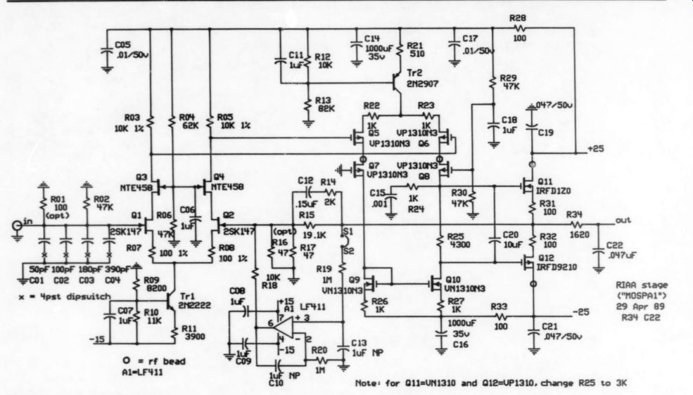
FIGURE 6: Complete RIAA stage.
Transistors
Before we carry the design of the RIAA section any further, I would like to consider the transistor elements which pro vide the active gain. As in my design of the MOS power amplifier, I wanted to see if there could be a benefit to the design from MOS technology. MOS units did seem to give favorable results in the power amp, and it would be very welcome to construct similar performance into the preamp.
As often happens in design work, one is not alone in certain thoughts; there is a two-way flow of ideas which in this case brought to my attention the existence of additional sources of MOS transistors attractive for audio use. In fact, it occurred as a result of the power amp design article, when in the letters to the editor section (TAA 3/88) K. E. Logan suggested that the Supertex line of MOS devices might be an improvement over the IRFD series I was using.
Thus, I have included a short study of the properties of several candidate n channel transistors for amplifier use (see the sidebar, 'Some Amplifier Device Properties''). I intended originally to develop a simple math model for com parison of the Supertex and IRFD types, but I found it interesting in its own way to add some JFETS (the ones previously mentioned) and to include the well known vacuum-tube, the 12AX7 (ECC83).
The results in the sidebar support the use of either of the MOS types for volt age amplifiers, particularly in those parts of the circuit requiring relatively high voltage swings and larger currents.
I have used MOS devices in all the positions subsequent to the JFET input stage of the RIAA section, and in the like parts of the tape and line drivers. MOS units are surely useful for output transistors as well, since they re easily able to sup ply whatever currents the lines require.
Design I built the RIAA stage using p-channel MOS devices following the cascode of …
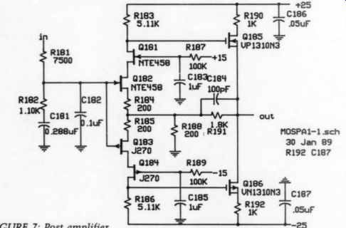
FIGURE 7: Post amplifier.
… input stage JFETs. See the complete circuit of the RIAA stage in Fig. 6. This p channel stage, Q5 through Q8, faces in to a current mirror of n-channel MOS units, Q9 and Q10, either the 1Z0 or the VN1310. The circuit board layout suggested later is able to accept either of these types. To balance the signal cur rents, the current mirror uses relatively large common-source resistors R26 and R27. A randomly selected pair of can't be expected to balance very well, and it certainly is not a very desirable circuit if one is required to search through a group to find two alike.
The current mirror therefore uses 1 k-O source resistors which bring the mirror into DC and AC balance with out requiring matching. This provides sufficiently close current balance to permit satisfactory control of the out put stage DC bias point and its signal drive (see the note on Fig. 6 for selection of the value of resistor R25).
This output stage, using a double source-follower n-channel and p-channel pair is also stabilized by using relatively large 100-ohm source resistors. The DC offset at the output is controlled by op amp servo Al. Predictable bias cur rents are generated at the input stage by transistor Tr1, and in the p-channel stage by transistor Tr2, which set up the bias points of the input stage and of the current mirror.
Feedback parts C12, R14 and R15 are connected from the output to the input feedback point and use 1% accurate parts for close conformity to the 50 and 500Hz RIAA response points. The response to the junction of R31 and R32 is flat beyond the 500Hz turnover frequency. Output RC R34 and C22 sets the 75uS rolloff, which is designed to drive a 100k load.
By paralleling R17 with an optional 47-ohm resistor, R16, the RIAA stage gain can be raised by 6dB in cases where a lower level MM cartridge is used. The 1kHz gain to the output of the RIAA stage is then approximately 38dB.
The combination of a low-voltage drop current supply from Tr2 for the positive end of the current mirror circuit, and a 2V loss in the current balance resistors R26 and R27 allows the RIAA output stage to operate over much of the + 25V power supply range. This output can thus tolerate output swings as high as +15V. To be conservative, + 10V of output swing allows an over load input at 1kHz of as high as 250mV peak from the phono cartridge.
The detail of the input circuit of Fig. 6 shows a group of terminating capacitors C01 through C04. These are arranged in a progression of values to cover the range of 50 to 720pF in 50pF steps. With a DIP switch selecting combinations of these four capacitors, about any terminating capacitance likely to be needed is available.
An optional low-resistance terminator R01 can be soldered into the circuit...
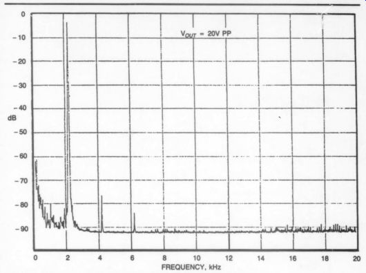
FIGURE 8: RIAA post amp and line amp: harmonic plot.
...board to convert the RIAA input to use with some of the higher-output moving coil cartridges. I did not use a DIP switch in conjunction with this option because of the probable infrequent use of the feature, and because the switch contact resistance might be able to introduce a little nonlinearity when com pared to the low resistance of R01.
Post-Amplifier Stage
The conversion of the pre-amp to a fully passive RIAA stage requires a moderate gain post-amplifier, as mentioned. This stage is only required to drive the level control and is not expected to be connected to any output lines. Thus it can have a moderate output impedance. I included a minimal-complexity circuit to provide a signal gain of about 6:1 or 16dB, and to buffer the passive network from any load effect (Fig. 7). It makes use of the same n- and p-channel JFETs as the line driver circuit to be described.
A cascode of these J-FETSs drives a simple MOSFET output stage. The bias current level for this output stage is set up by the characteristics of the JFET in put pair at about 4mA, so no heatsinks are needed.
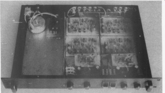
------------Photo 3
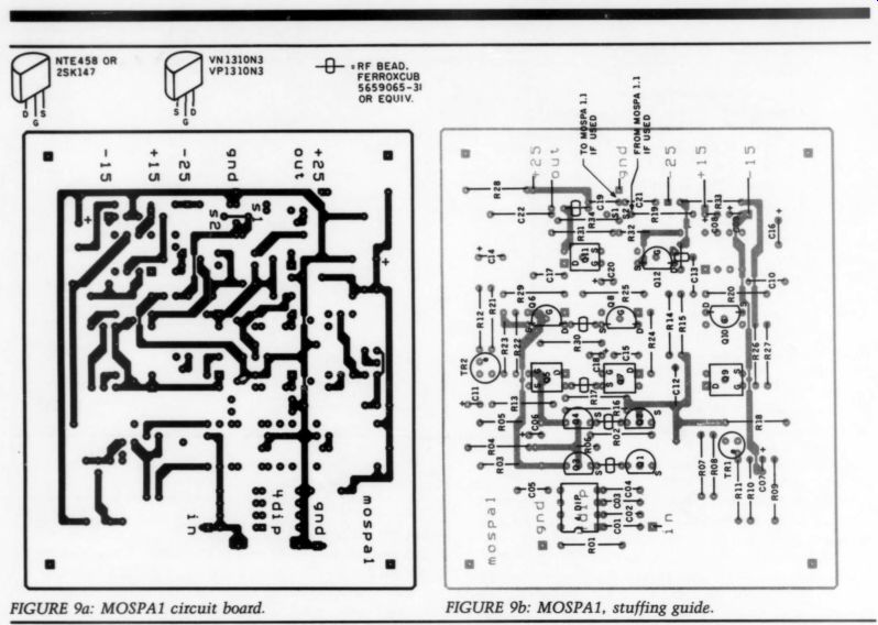
FIGURE 9a: MOSPAI1 circuit board. ----Fig 9b
The circuit provides flat gain within 1dB from DC to about 250kHz and has arise time of about 0.3uS. The harmonic distortion of this circuit shows no visible component lines above the noise level at 90dB below a 1V peak signal.
At 10V peak, the harmonic con tent is seen above the noise, but is less than 75dB below the signal peak (Fig. 8). This circuit includes the passive net work on a small circuit board, which can be stacked above the associated in put circuit board, and mounted on two of the same mounting standoffs. A shield plate of one-sided circuit board material can be sandwiched between the two layers and grounded to the post amp circuit ground to avert signal crosstalk.
If used, this circuit's input at the 7,5000 resistor is connected to the junction of R31 and R32 of the circuit of Fig. 6, and two changes are made: resistor R34 is removed to eliminate the loading effect of the 75uS RC, and capacitor C12 is shorted. These changes convert the main amplifier section to a flat gain stage, leaving the entire frequency con touring to the passive parts mounted on the post-amp board. The output of the post-amp is then connected to the phono tap of the selector switch in place of the former signal from C22 of Fig. 6.
To servo the DC output of the post-amp to zero, it is only necessary to move the sample point of servo amplifier A1 of Fig. 6 to include the post amp.
To do this, remove jumper S1-S2 on the MOSPAL circuit board and connect a wire from the output of the post-amp to the S2 end of resistor R19. This will cause the servo to make the necessary slight change required to balance out the offset of the post-amp, which will probably require only a few millivolts
PARTS LIST
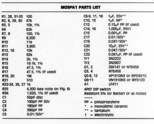
MOSPA1
Resistors 5% (or Better) or as noted
PP = polypropylene
= monolithic ceramic
= tantalum
= electrolytic
--------------
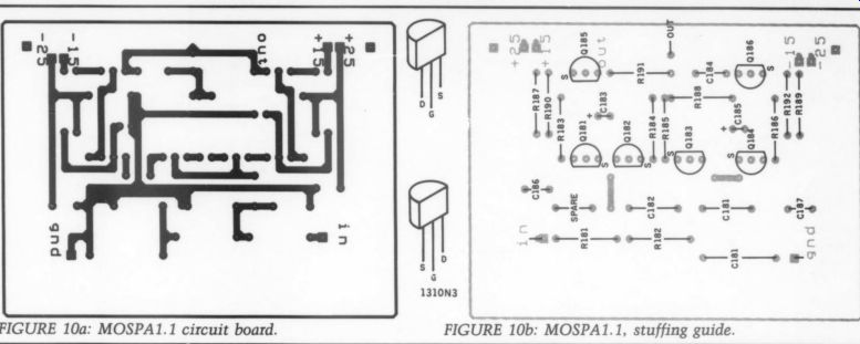
FIGURE 10a: MOSPA1.1 circuit board.
FIGURE 10b: MOSPA1.1, stuffing guide.
change at the old S1 sample point. The servo operates as before, since the DC gain of the whole servo loop including the gains of Figs. 6 and 7 together, is no greater than it was originally for Fig. 6 alone, since C12 has now been shorted.
The suggested circuit board layouts for the RIAA main section circuit, and for the optional post-amp equalizer circuit are given in Figs. 9a and 10a. The associated stuffing guides are given in Figs. 9b and 10b.
Line Driver
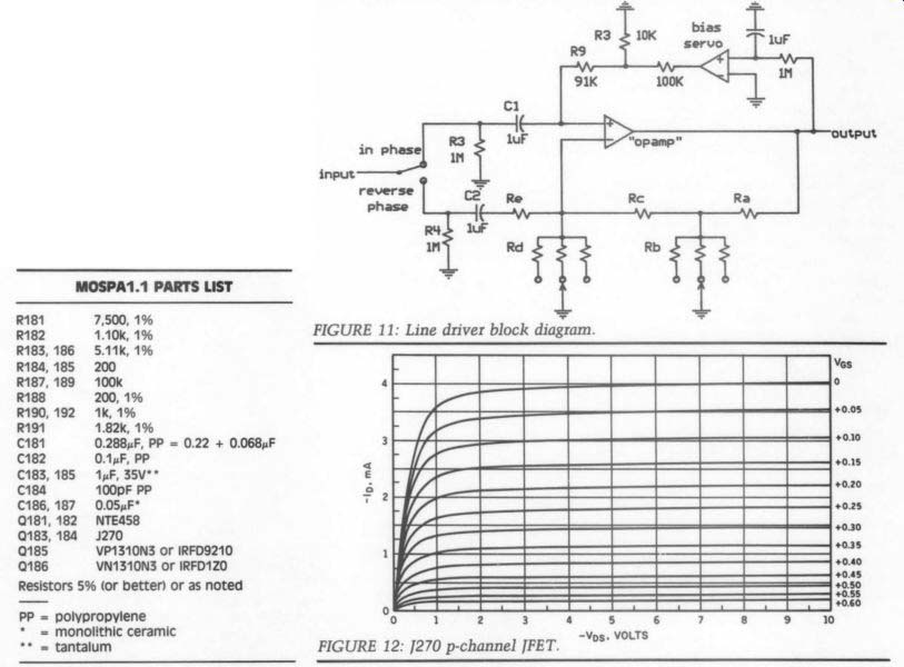
When it comes to the design of the line driver stage, we must meet several requirements. Figure 11 is the basic circuit idea. The "op amp'' will of course be constructed using discretes of JFET and MOS types. The phase-reversing in put is the negative input of the ''op amp'' and presents the resistance Re to the input source. The reverse-phase in put shouldn't be grounded when in phase gain is chosen. Doing so would raise the gain of the channel; we want equality of gain in both phases. We could switch in a 6dB pad, but this would raise the noise level of the system.
The circuit of Fig. 11 allows the choice of any of three different in-phase and reverse-phase gains, while retaining equal signal gain for either phase. The gain is changed by varying only those resistors that connect to ground, so no floating switched parts are required.
--------------
MOSPA1.1 PARTS LIST
-------------------------------
FIGURE 11:
FIGURE 12: J270 p-channel JFET.
FIGURE 13: Line driver circuit.
----------------
No impedance change should be seen by the input source. By making Re equal to R9 at the in-phase input, we prevent the change of input resistance that would occur when switching this circuit from in-phase to reverse-phase gain. This problem could have been rendered a minor effect by letting Re be about 1 megohm, but Re can't be so large-it limits the noise level of the circuit even when set to 100k. The chosen impedance level of 100k is a compromise between noise and reflecting too low an impedance back to the level control.
The line amp gain is to be set to any of three values, +12,+ 18 or+24dB, selected by switching three sets of values Rb and Rd. We expect the maximum output level to be about 1 to 3V, the level required to drive the power amplifier to its limit. A system gain of zero dB is thus achieved when the level control is set for an 18dB loss. This makes an 18dB reserve of gain avail able, which is a comfortable setting.
For lower level input signals, the higher step of line amp gain can be used. At the intermediate setting, there is an 18dB noise gain in the line amp, even if the level control is set to zero.
A noise output 18dB above the noise of the two 100k resistors, Rc and Re, is to be expected. The noise of these two resistors at room temperature is about 10xV RMS in a 30kHz bandwidth; 18dB above this is a noise level of 80uV RMS, which is 82dB below 1V. This provides
--------------------
LINE DRIVER PARTS LIST
-----------------------
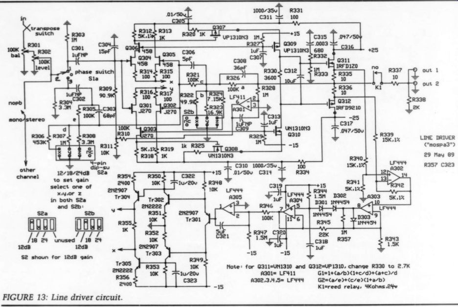
Figure 13
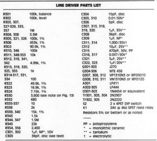
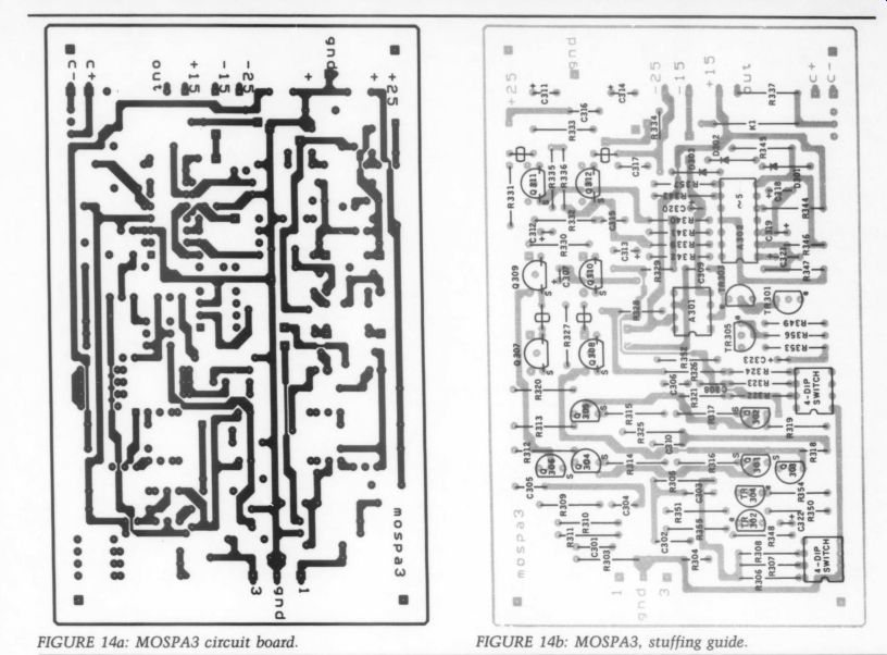
FIGURE 14a: MOSPAS3 circuit board.
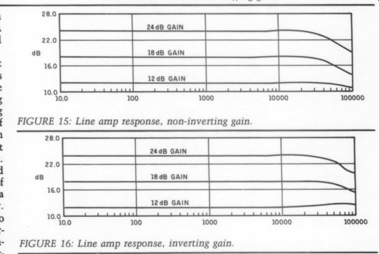
FIGURE 16: Line amp response, inverting gain.
... an 82dB dynamic range in combination with a 1V to full power amplifier. A larger than 1V to full power system will of course raise this specification.
DC blocking capacitors C1 and C2 at the line driver input are sometimes scorned. Their purpose is to prevent the possibility of an input signal providing an unwanted DC component along with the input signal. Since all sorts of other input systems might be used with the preamp, I thought it wise to protect the line driver from a DC-bearing input.
If a DC voltage were to be applied across the level control, then the act of varying the level setting would send a varying DC level to the line driver.
This would likely cause the bias servo in the line driver to slew around in correction, causing bias errors and accompanying distortion to occur. This blocking capacitor at the input has the benefit of allowing us to locate the bias servo at the positive input of the circuit instead of the usual negative (feedback) input. This not only makes the servo simpler (it can be constructed with one RC instead of the usual two), but also
it allows another design advantage: the avoidance of clicks when operating the phase switch.
The bias servo must be able to apply small DC levels to the positive input.
This bias is blocked from appearing at the input, that is at the level control, which is not a fixed resistance to ground. The servo would have a problem acting in the presence of such a connection. In general, C1 and C2 will have different DC voltages across them,
that on C2 being the result of small leakage currents in the input gates.
Thump- and click-free switching of the phase selector results from keeping these small DC voltages on C1 and C2 with resistors R3 and R4. Further, this allows the circuit to operate with no bias voltage across the gain resistors Rd.
Thus, experiments with gain can be click-free as well.
Now let's consider the detail of the op amp of Fig. 11. Here I have used a differential n-channel-p-channel input stage. This arrangement has great acceptance in recent designs, and with good reason; it is very linear and can be worked into a balanced driver and balanced output stage design which pro vides very good utilization of the headroom offered by the power bus voltages.
The n-channel-p-channel input stage has one difficulty: the n and p devices need to be fairly equal in bias and gain.
Few such matched JFETs exist. The best choice appears to be the previously mentioned 2SK147 and its p-channel counterpart 2S]72. These would be used here if these units were more readily available.
I chose instead to design around the NTE458 because of its availability.
Now we need a p-channel to balance against the 458. Luckily, the J270 p channel JFET is a good candidate for the purpose (Fig. 12). This unit is available from Newark, and is the linear characterization of the 2N5114 switch transistor which might also satisfactorily balance with the 458.
The complete line driver design, shown in Fig. 13, makes use of these 458 and J270 JFETs in a cascoded push pull arrangement. I used MOS devices, also cascoded, as the driver stage and output stage. Good output linearity up to + 15V peak is available from this arrangement. Because the circuit is actively biased (as described shortly) to operate in the linear region, the circuit can operate into a Class AB condition to provide up to 500mA peak into a 100 load. The transistors and other parts in the signal path are not thermally arranged to provide this much power continuously, but the current capability is there for the occasional dynamic signal peak! The line driver has this other duty to perform: we want it to supply relatively large currents. To provide this feature I made the output stage of the line driver into a low-level power amplifier, requiring a bias servo and some relatively low-resistance current-sampling resistors to operate it. I adapted the bias idea described in my 40W MOSFET power amplifier design for use in set ting up the output stage current level.
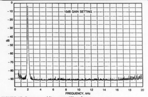
FIGURE 17: Spectrum of line amp, 1V peak out.
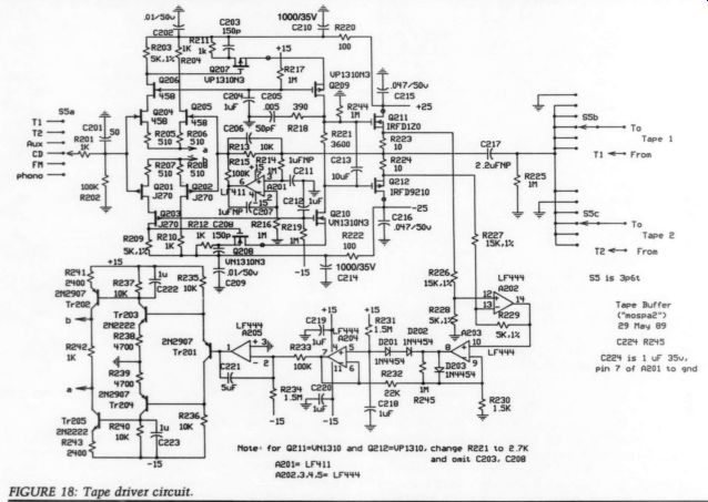
FIGURE 18: Tape driver circuit. Note: for G211=UN1310 and G212=UP1310, change R221 to 2.7K A201= LF411 A202.3.4.5= LFY44 and omit C203, C208
------------- TAPE DRIVER PARTS LIST
--------------------
FIGURE 19: Spectrum of tape driver.
A comparison of the circuit of Fig. 13 with the circuit of the power amplifier will show a likeness up to the output of servo op amp A4 (here A305).
The preamp circuit version needs a balanced correction current, however.
This is provided by transistors Tr301 305. When the circuit first comes into operation, input transistors Q301-306 can only pass the current determined by R355, which is insufficient to set up enough bias at R312 and R318. The result of this temporary balance is that output stage operating current is zero or very small. A few seconds of time elapses while a charge builds up in C321 in the control amplifier A305.
This gradually raises the input stage conduction until all the loop biases settle at the design values.
A current flow of 10mA DC is thus established in output transistors Q311 and Q312, and at the same time all the DC operating points in the driver stage and input stage are held fixed (see the note on Fig. 13 on selection of the value of resistor R330). The somewhat complex nature of all this circuitry is justified by this result, since no control part is actually part of the signal path, which is itself quite straightforward.
A signal path gain of 12, 18 and 24dB is selected by gain switch S2, a 2P3T rotary switch located on the rear panel of the prototype chassis. This scheme allows switch-selected gain experiments. The circuit board layout to be described adds DIP switches to the boards instead of the off-board rotary switch. This makes it a matter of sys tem setup to preset the gain switches before closing the cover. Either arrangement is possible with the board layout shown.
I encountered a problem in the line driver prototype. The trouble was not with the circuit operation, but at turn off, I observed a transient which I could not eliminate by the usual manipulation of the bias servo, or by variations in the stabilization networks. I saw that some LF444s can burst into oscillation when the 15V power bus decays to a very few volts. This can send a signal to the output, resulting in a noise burst during the power-off sequence.
------------------- the discussion. We then pointed out that the pre amp alone had driven the speaker without benefit of a power amplifier. Of course, the 103dB efficiency horn loudspeaker system connected directly to the preamplifier output made this possible.
------------------ FIGURE 20a: MOSPA2 circuit board.
Since it is possible that the preamp power might be switched off before the associated power amplifier, any preamp output signal might be amplified, even with the level control turned to zero.
This might not be a problem in systems having a common power line switch, but I wanted a better method. There fore I included a reed relay which drops out when the power bus lines are still at about 75% of full value, thus masking from the output any unwanted shut down signals. The relay contact resistance is small compared to R338 (2k).
You can bypass the relay if you wish.
Figure 14a, the 4.25 x 5.25" circuit board layout for the complete line driver, contains all the features de scribed, including the reed relay and DIP switches for selecting gain. Figure 14b is the stuffing guide.
YOUR MAGIC NUMBER HELPS US ANSWER FASTER
This number. which appears in the upper left corner of your mailing label. is your key to a speedy reply.
Performance curves for this circuit are given in Figs. 15 and 16. The response is flat to within 0.5dB or better to 30kHz at all gain settings. Harmonic distortion, plotted in Fig. 17, is quite acceptably low.
Tape Drivers
A usable preamplifier of the subsystems described so far can be assembled. The missing element is a tape loop driver, which you need if you are using any out board equipment. This circuit should have a signal gain of unity, and it is likely that the load of cables might be even greater than on the main line output.
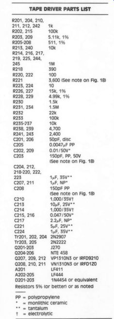
For the tape driver circuit, I used a simplified line driver. The circuit in Fig. 18 is a unity gain version, without the inverting phase input. The DC blocking capacitor is at the output rather than at the input because this output is liable to be connected to any of a wide variety of equipment, which might introduce a DC offset voltage or a power-down short.
The bias servo is connected to the feedback return side of the input stage and can provide for enough offset to equal a DC input of up to 1V. I used the same balanced-bias control circuit designed for the line driver which sets the DC operating points of the transistors as before (see the note on Fig. 18 on selection of the value of resistor R221). The frequency response of this circuit is down 3dB at about 150kHz, with a rise time of about 0.8uS. The harmonic distortion curve is given in Fig. 19.
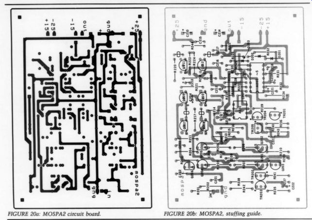
Figures 20a and 20b are the board lay out and stuffing guide for the 4.25 x 4.5" card.
Part 2 of this article covers the assembly of the preamp as well as the power supply. A critique by three listeners is also included. If there is sufficient reader interest , I will make the circuit cards and a kit of parts available for this project.
++++++++++++++++
Also see: