A power supply converts the ac input of the 60-Hz power line to dc output voltage. The television receiver has two power supplies. One is the low-voltage supply for B+ voltage and heater power for tubes. The other is a high-voltage supply for the anode voltage of the picture tube. The total amount of power used from the 120-V ac line is about 150 W in monochrome receivers and 250 W in color receivers. For vacuum tube amplifiers, the B+ voltage generally is about 140 to 280 V for plate and screen voltages. For transistors, the required collector voltage is 15 to 100 V. In the high-voltage supply, the required anode voltage is 10 to 20 kV for monochrome or 15 to 30 kV for color picture tubes. The rectifier that converts the ac input to dc output is generally a silicon diode (Fig. 12-1). Methods of using diode rectifiers in different types of power supplies are explained in the following topics:
12-1 Basic functions of a power supply
12-2 The B+ supply line
12-3 Types of rectifier circuits
12-4 Half-wave rectifiers
12-5 Low-voltage supply with half-wave rectifier
12-6 Full-wave center-tap rectifier
12-7 Full-wave bridge rectifier
12-8 Voltage doublers
12-9 Voltage triplers and quadruplers
12-10 Heater circuits
12-11 Filter circuits
12-12 Voltage regulators
12-13 Low-voltage supply with series regulator circuit
12-14 Troubles in the low-voltage supply
12-15 Hum in the B+ voltage
12-16 Flyback high-voltage supply
12-17 Fuses and circuit breakers
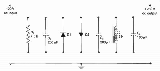
FIGURE 12-1 SILICON-DIODE RECTIFIERS. ACTUAL SIZE, WITH SCHEMATIC SYMBOL BELOW.
FROM LEFT TO RIGHT, HIGH-HAT, PELLET, AND STICK TYPES.
12-1 Basic Functions of a Power Supply
Basically, all that the power supply needs is a rectifier to change the ac input to dc output.
However, filter capacitors generally are used to remove the pulsating variations from the dc output voltage of the rectifier. In addition, a power transformer is often needed to step up or step down the ac input voltage. Finally, a voltage regulator may be used, especially with transistor circuits. A regulator keeps the dc output voltage constant when the dc load current changes.
These basic functions are illustrated by the block diagram in Fig. 12-2. The supply is shown with positive dc output for B+ voltage. Positive polarity is needed for plate and screen voltages or tubes and collector voltage on NPN transistors.
The rectifier. Because it conducts in one direction, a rectifier converts its ac input to dc output.
The current flows only for the polarity of input voltage that makes the anode positive. Or, negative cathode voltage makes the diode conduct.
A single diode is a half-wave rectifier, as it can conduct only for a half-cycle of the ac input.
Power supplies generally use silicon diode rectifiers (Fig. 12-1). The current rating is 500 mA for the smallest diodes up to 10 A or more. Larger units are stud-mounted. The advantage of a silicon diode is its very low internal voltage drop of 1 V or less, compared with 18 V, approximately, for a vacuum tube diode. Silicon diodes are generally labeled D, SD, X, Y, or CR for crystal rectifier.
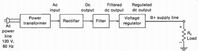
FIGURE 12-2 BASIC FUNCTIONS OF A POWER SUPPLY, WITH POSITIVE DC OUTPUT VOLTAGE
Note the schematic symbol in Fig. 12-1 for a semiconductor diode. The arrowhead is the anode, while the bar is the cathode, corresponding to plate and cathode in a vacuum tube.
On the diode unit, a bar, circle, or dot indicates the cathode terminal. The direction of the arrow shows hole current, as the forward current, from anode to cathode. Remember that hole current is a motion of positive charges, however, in the opposite direction from electron flow.
Peak reverse voltage (PRV). This is the maximum voltage that can be applied in the nonconducting direction, with the anode negative. Too much reverse voltage across the rectifier can produce breakdown at the junction, resulting in a shorted diode.
The actual amount of reverse voltage across a diode rectifier is about twice the dc output voltage, as shown in Fig. 12-3. In addition to the negative ac input at the anode, the dc voltage at the cathode is series-aiding, when you consider the potential difference across the diode. Typical PRV ratings for small silicon diodes are 400 to 1,000 V. Checking the rectifier. A semiconductor diode can be easily checked with an ohmmeter to see if it is open or shorted. Out of the circuit, just measure the diode resistance in both directions by reversing the ohmmeter leads. The diode resistance should be very low in the forward direction and at least 100 times higher in the reverse direction. If the resistance is very low in both directions, the diode must be shorted. If the resistance is very high in both directions, the diode must be open. When an ohmmeter is used to check the diode in the circuit, make sure that the power is off, the filter capacitors are discharged, and one side of the diode is disconnected.
Filter. Although the dc output of the rectifier has only one polarity, the rectified voltage still includes the amplitude variations of the ac input.
This ac component is called ripple in the dc output voltage. A filter can eliminate practically all the ripple.
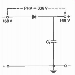
FIGURE 12-3 PEAK REVERSE VOLTAGE (PRV) ACROSS RECTIFIER DIODE.
Voltage regulator. Voltage regulation means maintaining a constant dc voltage output, even when the ac input voltage increases or de creases, or when the dc load current changes. A voltage regulator is often included in the low voltage supply to maintain constant height and width in the scanning raster. For the high-voltage supply in color receivers, a regulator is used to prevent changes in focus and convergence for the color picture tube.
Power transformer. The ac voltage needed may be more or less than the 120 V of the 60-Hz power line. Then a power transformer is used (Fig. 12-4). By mutual induction between L_p and L_s, the ac secondary voltage is stepped up or down in direct proportion to the turns ratio. The isolated secondary in a has no connection to the primary, as two separate windings are used. In an autotransformer, such as in b, one winding is used for both L_s and L_p. The tap makes L_p just a part of the entire coil with L_s. Therefore, L_s is not isolated from L. Where the coil is tapped deter mines the turns ratio.
With either type of transformer, the power supply can operate only with ac input. This type is called an ac power supply, which only means that it has a transformer requiring ac voltage. A supply without a transformer is connected directly to the power line for ac input voltage. This type can operate on either ac input or dc input of the correct polarity that allows the rectifier to conduct. Actually, the dc input does not have much meaning because very few homes have a dc power line. However, the name "ac-dc power supply" is used to indicate there is no power transformer.
Isolation. A supply that has a power transformer with a separate secondary winding is isolated from the ac power line. The primary is connected to the ac line, but the rectifier circuit with dc output is in the secondary. The receiver chassis, which is usually B- for the dc output, then, is a "cold" chassis because it is isolated.
This type is called a line-isolated supply.
With an autotransformer or no power transformer at all, however, the receiver chassis can be "hot," meaning it is connected to the high side of the ac power line. Then there is danger of electric shock when touching the receiver chassis or exposed metal parts. This type is called a line-connected supply.
Portable receivers generally use a line connected supply. The purpose is to eliminate the size and weight of the power transformer.
Remember that the ac power line has one side connected to earth ground, while the other side is the live connection. If the ac plug is inserted in the polarity that connects the receiver chassis to the live side of the ac power then touching the chassis is the same as touching the 120-V power line.
To avoid this danger in a power supply which is not isolated, plug the receiver into the ac outlet with the grounded side connected to the receiver chassis. Many receivers now have a plug with one wide tip. It can be plugged in only the one way that grounds the chassis.
However, a polarized type of socket is necessary to take this plug.
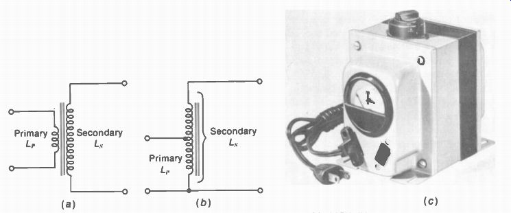
FIGURE 12-4 POWER TRANSFORMERS (a) SCHEMATIC WITH ISOLATED SECONDARY (b) AUTOTRANSFORMER,
WITH SECONDARY NOT ISOLATED. (c) ISOLATON TRANSFORMER WITH VARIABLE OUTPUT
VOLTAGE AND METER FOR TESTING RECEIVERS. (TRIAD-UTRAD)
Isolation transformer. This power transformer has a 1:1 turns ratio with an isolated secondary winding. It is a good safety practice to use the isolation transformer when testing a receiver that has a line-connected power supply. The wattage rating should be 250 W or more, for color receivers. The transformer can also be made with a variable turns ratio. Its purpose is to test the receiver with voltages higher or lower than normal. See Fig. 12-4c.
12-2 The B+ Supply Line
Although tubes and transistors generally amplify ac signals, they must have dc electrode voltages in order to conduct any current at all. These operating voltages are provided by the B+ voltage from the low-voltage power supply. For tubes, they use the B + for plate and screen voltage. Each stage has a separate path returning to the B+ supply line. These paths are in parallel with each other. For transistors, the branches for collector supply voltages are in parallel.
The details of a B+ supply line are shown in Fig. 12-5 for transistors. Only two transistors Q1 and Q2 are indicated here, but the same idea applies to all transistor stages operating from this low-voltage supply. For the example of Q1, its collector returns through R, to the 28-V supply. R, is the collector load resistor. The collector current I c assumed here for Q1 is 10 mA. It is important to note that the base voltage for Q1 is also taken from the B+ supply. The required forward bias between base and emitter is only a few tenths of a volt, but the R„ R4 voltage divider provides the voltage across R4 needed for the base. A bleeder current of 1 mA is assumed through the R„R4 branch.
Similarly, R, is in a parallel path for the collector of Q2. Also, the F1 . 5R6 provides base voltage for Q2. The bleeder current in this branch is 3 mA. The total current in the four parallel paths adds up to 10 + 1 + 14 + 3 = 28 mA. This load current of 28 mA at 28 V is equivalent to a load resistance of 28 V/0.028 A, or 1 k-O, as shown at the right in Fig. 12-5. If there are 20 transistors instead of 2, and if the total load current is 280 mA, the equivalent load resistance will be 100 ohm for the low-voltage supply.
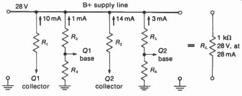
FIGURE 12-5 DETAILS OF THE B + SUPPLY LINE FOR TRANSISTOR AMPLIFIERS WITH
BRANCH CURRENTS DIRECTION SHOWN FOR ELECTRON FLOW
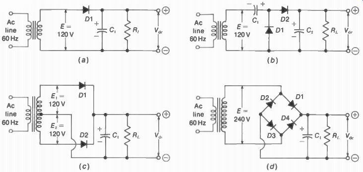
FIGURE 12-6 THE FOUR MOST COMMON TYPES OF RECTIFIER C.RCUITS. (a) HALF WAVE.
(b) HALF-WAVE VOLTAGE DOUBLER. (c) FULL-WAVE. CENTER-TAP. (d) FULL-WAVE BRIDGE.
12-3 Types of Rectifier Circuits
Figure 12-6 shows the four most common types: half-wave, half-wave doubler, full-wave center tap, and full-wave bridge. All the circuits are shown with an isolating power transformer, but they can be line-connected, except for the full-wave rectifier in c, which needs a power trans former for the center tap. The polarity is positive for dc output here, but it can be inverted by reversing the diodes.
The approximate amount of dc output voltage can be calculated, if we assume a silicon diode, the capacitor-input filter C _p and a typical load current of about 300 mA. The formula is:
141,. - 1 2 M (12-1)
The factor 1.2 is a constant for the specified conditions. Ern, is the ac input, which equals 120 V. Then the dc output voltage for the half wave rectifier in a is 1.2 x 120 = 144 V. For the voltage doubler in b, the dc output is 2 x 144 = 288 V. For the full-wave center-tap rectifier in c, the dc output is 144 V. We assume the total ac secondary voltage is 240 V, with 120 V for E1 and E2 to each diode.
In d, the full-wave bridge rectifier uses the entire ac secondary voltage for dc output voltage. Then the dc output here would be 288 V, with 240 V as ac input to the bridge.
The ripple frequency is 60 Hz for the half wave rectifier circuits in a and b, as one-half of each cycle of the 60-Hz ac input is used to produce dc output. For the full-wave rectifiers in c and d, the ripple frequency is 120 Hz because both halves of the cycle are used.
12-4 Half-Wave Rectifiers
The details of this basic circuit are illustrated in Figs. 12-7 to 12-11. The half-wave rectifier is fundamental to all types of power supplies because any one diode by itself can be only a half-wave rectifier. The other circuits are just combinations of half-wave diodes. A full-wave rectifier is really two half-wave diodes back to back, to conduct on opposite polarities of the ac input. A voltage doubler can be considered as two half-wave rectifier circuits that are effectively in series for dc output voltage.
Voltage polarities. See Fig. 12-7a and b for the opposite diode connections that make the dc output voltage either positive or negative. No filter capacitor is used here in order to show the basic waveforms of half-wave rectification.
Note the ac input is shaded to mark only the half-cycle that allows the diode to conduct. The diode in a conducts on the positive half-cycle, without any output for the negative half-cycle.
The dotted half-cycle in the waveform of voltage across R1 , indicates the part of the ac input that is missing in the dc output. In b, the diode connections are reversed to allow conduction on the negative half-cycle of the ac input, without any output for the positive half-cycle.
Positive dc output. In Fig. 12-7a, D1 conducts when the ac input makes the diode anode positive. When the diode conducts, it connects the high side of R1 , to the positive side of the ac source. The secondary winding L s on the power transformer is the source supplying ac input to this rectifier circuit. Electrons flow from the grounded side of L s . up through R, and from cathode to anode in Q1, returning to the positive terminal of the ac source at the top of L. As a result, the top of R1 , is the positive side of the voltage drop V RL . The basic reason is that when the diode conducts, it connects the high side of R1 , to the high side of L s only when this point has positive ac input voltage.
Negative dc output. In Fig. 12-7b, D1 conducts when the ac input makes the diode cathode negative. Note that the ac input voltage is reversed now. Making the cathode negative is equivalent to making the anode positive.
FIGURE 12-7 HALF-WAVE RECTIFIER CIRCUITS WITHOUT FILTER. (a) POSITIVE DC OUTPUT. (b) DIODE RE VERSED FOR NEGATIVE DC OUTPUT.
With the diode conducting in Fig. 12-7b, we can consider electron flow starting from the top of L s, from cathode to anode in D1, through R_L and returning to the grounded end of L. As a result, the top of R1 , is the negative side of the voltage drop V_RL . A fundamental way to consider the negative dc output voltage in b is the fact that when the diode conducts, it connects the high side of R_L to the high side of L_S only when the ac input is negative.
The negative dc output voltage in Fig. 12-7b is negative with respect to chassis ground.
There is no law that says chassis ground must be the most negative point. The polarities are determined by the source supplying the ac input.
In this circuit with negative dc output voltage, chassis ground is actually positive because the ac input is positive at the grounded end when the diode conducts.
The two polarities for dc output voltage can be summarized briefly as follows:
1. Connect the ac input to the anode of the diode for positive dc voltage at the load in the cathode circuit.
2. Connect the ac input to cathode of the diode for negative dc voltage at the load in the anode circuit.
Line-connected half-wave rectifier. No power transformer is used in Fig. 12-8 for the typical case of a half-wave power supply that is not isolated from the power line. C, is the filter capacitor to remove the 60-Hz ac ripple from the dc output voltage. The capacitor input filter is necessary to provide dc output voltage during the time when the diode is not conducting.
R, in series with Q1 is used as a surge protection resistor. It limits the peak current through the diode when C, is charging. The resistance is generally 3 to 7 ohm, with a power rating of 5 W. When a power transformer is used, R, is not needed because the secondary winding has the required series resistance.
This circuit has positive dc output at the cathode for B+ voltage. The ac input is applied to the anode. Note that the B - side of the power supply is connected to the grounded, or neutral, side of the ac input from the power line, to reduce shock hazard.
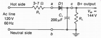
FIGURE 12-8 LINE-CONNECTED HALF-WAVE RECTIFIER. WITH FILTER.
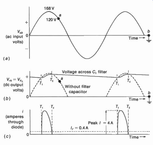
FIGURE 12-9 WAVEFORMS OF HALF WAVE RECTIFIER. (a) AC INPUT VOLTAGE V_ab (b)
DC OUTPUT VOLTAGE V_ab OR VOLTAGE ACROSS R_L. (c) CURRENT THROUGH DIODE
Effects of the filter capacitor. In Fig. 12-8, C, charges fast through the very low resistance of the rectifier diode when it conducts, but discharges slowly through the load resistance. As a result, C, maintains the dc output voltage during the half-cycle when the diode is not conducting.
In this process of fast charge and slow discharge, the filter capacitor has the following effects:
1. The 60-Hz ac ripple is practically eliminated from the dc output.
2. The dc output voltage is maintained during the entire cycle of ac input.
3. The dc voltage across C, puts reverse bias on the diode so that it can conduct only at the peak of the ac input. As a result, the diode is a peak rectifier.
The waveforms in Fig. 12-9 illustrate the diode operation with the input filter capacitor.
In a, the sine-wave voltage is shown for the ac input across terminals a and b in Fig. 12-8. Note that 120 V is the rms value of the sine wave, while the peak value is: 1.4 x 120 = 168 V
The waveform in Fig. 12-9b shows the dc output voltage across C1 and R1 , in parallel. This voltage is labeled V eh between points c and b in Fig. 12-8. Assume the circuit has been operating for a few cycles of the ac input to charge C1. Then the diode is forward-biased just for the time from T1 to T2. Only during this period does the ac input voltage make the diode anode more positive than the dc output voltage at the cathode. Remember that positive voltage at the diode cathode is reverse voltage that prevents conduction.
During the short conduction time from T1 to T2, a large pulse of current flows through the diode and the ac input circuit to charge C1. As a result, the voltage across the capacitor rises rap idly. The time constant is short with the very low resistance of the forward-biased diode. The peak capacitor voltage is practically equal to the peak value of the ac input voltage, minus the 1-V drop across the silicon diode.
After the time T2, the ac input voltage is not positive enough to forward-bias the diode, and it stops conducting. The diode is then an open circuit, and it cannot charge C1. Then C1 discharges slowly from time T2 to T1 through the relatively high resistance of the load RL. This same sequence of fast charge and slow discharge for C, is repeated every cycle. As a result, Vet, across C, and RL in parallel is a relatively steady dc output voltage, with a very small component of 60-Hz ac ripple.
Charge and discharge current. The peaks of current that flow through the diode to charge C, are shown in Fig. 12-9c. A peak value of 4 A is shown here. This figure is 10 times the typical forward current (l r) of 400 mA or 0.4 A assumed for the load.
The path for charging current is shown in Fig. 12-10a. Here electrons flow from point b of the ac input to charge the low end of C, negative. Electrons repelled from the positive side of C, flow from cathode to anode in the diode and return through R, to point a at the source. It is important to note that the higher the capacitance of the filter C, is, the higher is the peak value of the charging current through the diode.
In Fig. 12-10b, C1 discharges through R_L when the diode is not conducting. Now the circuit consists only of C1 and R_L. The diode is an open circuit, and it effectively disconnects the ac input. This discharge occurs between times T2 and T1 in Fig. 12-9. Actually, the filter capacitor supplies the current to the load for about 90 percent of the time, while the diode is not conducting. During the 10 percent of the cycle when the diode is on, it allows the ac input voltage to charge C1 while supplying the load current.
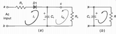
FIGURE 12-10 CHARGE AND DISCHARGE OF THE FILTER CAPACITOR C1 IN HALF-WAVE
RECTIFIER. (a) DIODE CHARGES C, BETWEEN TIMES T1 AND T2 ON WAVEFORMS IN FIG.
12-9. (b) C, DISCHARGES THROUGH THE LOAD BETWEEN T, AND T, WHEN DIODE IS NOT
CONDUCTING.
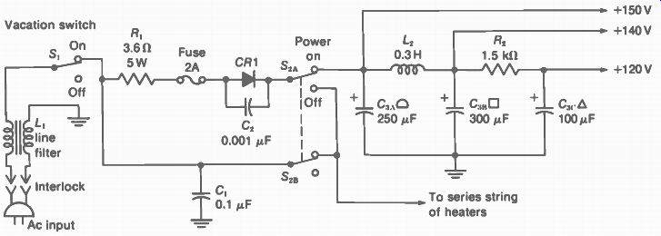
FIGURE 12-11 TYPICAL LOW-VOLTAGE POWER SUPPLY WITH LINE-CONNECTED HALF WAVE
RECTIFIER AND SERIES HEATERS FOR VACUUM TUBES. (GE CHASSIS D2)
12-5 Low-Voltage Supply with Half-Wave Rectifier
These circuits are usually line-connected ac-dc supplies, without a power transformer. All the heaters, including the picture tube, are in a series string with voltage ratings that add up to the 120 V of the ac power line.
In Fig. 12-11, CR1 is the silicon half-wave diode rectifier. The diode is connected to the ac power line through the 3.6-ohm surge-protective resistor R1, a 2-A fuse, and the switch S1. With ac input to the anode of CR1, the positive half cycles are rectified to produce positive dc output at the cathode. The B+ voltage at the input filter capacitor C3A is 150V. A two-section filter is used with the 0.3-H filter choke L2 and 1.5-k-ohm filter resistor R2. The output filter capacitor is the 100-uF C3c, while the 300-uF C3B is the midsection filter capacitor. All three filters are electrolytic capacitors in one can with the half circle, square, and triangle marks to indicate each section.
In the dc output voltages, note that 140 V is less than the unfiltered B+ voltage of 150 V because of the 10-V drop across the dc resistance of L. Also, the voltage drop of 20 V across R2 reduces the filtered output voltage from 140 to 120V. Quick-on operation. Many receivers with tubes now have instant-on, instant-view, or quick-on operation for the heaters. This feature allows the heaters to be on with half power, when the receiver is off. Then, when the receiver is turned on, full power is applied to the heaters. The picture and sound come on almost instantly because the heaters are not cold.
Referring to Fig. 12-11, the switches S1 and S2 apply power to the receiver. S1 is the "vacation switch." When the receiver is not used for a long period, S, is opened to prevent any power being applied. Normally, though, S1 is closed. Then the ac input is connected to the power supply, but the on-off switch S1 determines how. With S _p open, the filtering circuit is open for no B+ voltage. However, then CR1 is connected by S2A to the series string of heaters.
As a result, the positive half-cycles of the ac input are used to operate the heaters at half power. Then the heaters are warm and the tubes are in a ready state to be turned on quickly.
When the power switch is closed to turn the set on, S2A completes the rectifier circuit for B+ voltage. Also, the lower section S2A connects the heater string directly to the ac line for full power. The quick-on circuit shortens the turn on time of the receiver from 30 s or more to 2 s or less.
Hash filter. Interference from motors, neon signs, or any sparking contacts is called hash because it does not have a specific resonant frequency. In order to filter any hash interference, either into or out of the power line, the line filter L, is used with C, as in Fig. 12-11. L, is a balanced choke with series inductance in both sides of the line. A typical value is 1 mH.
Silicon hum bar. When the silicon diode con ducts, a large pulse of charging current flows in the ac input circuit. You can see this pulse with an oscilloscope across the surge-limiting resistor. The repetition rate of the pulses is 60 Hz. Because of its fast rise time, the pulse can radiate interference into the rf, IF, or video circuits. The result then is a black or white horizontal bar across the picture. This bar can be shifted between top and bottom of the picture by reversing the ac plug. To minimize the interference, a silicon-diode rectifier usually has a 0.001-µF shunt capacitor such as C2 in Fig. 12-11. In addition, a large value can be used for the hash filter capacitor C1.
Ac power interlock plug. When the back cover of the receiver is removed, the ac power cord is disconnected. In order to operate the receiver with the cover off, a "cheater cord" is used, which is a substitute line with its own plug.
Some interlocks have one pin bigger than the other, for a polarized plug. The wider pin is the ground side.
12-6 Full-Wave Center-Tap Rectifier
This circuit uses two diodes to rectify both half cycles of the ac input. Each diode is a half-wave rectifier, but they have a common load Rt. See Fig. 12-12. Only one-half the total secondary voltage is used for each diode, from each end of L_s to the center. A power transformer is needed to provide the center-tap.
It is important to note that opposite ends of a coil always have opposite polarities with respect to the center. When the top end of L_s is positive, the bottom end is negative, as shown in Fig. 12-12a. For this polarity of ac input, the anode of D1 is positive, and this diode conducts.
On the next half-cycle, though, all the polarities are opposite. Then the bottom of L s is positive to make the Q2 anode positive, and the bottom diode conducts.
When diode 1 conducts, we can trace the electron flow of I_1 from the center-tap, through Rt, from cathode to anode in D1 and returning to the top of L. Therefore, the cathode side of R_L at the right is the positive side of V_RL with respect to the grounded center-tap, which is B-. See the top waveshape in Fig. 12-12b.
On the next half-cycle, diode 2 conducts.
The electron flow of I_2 is from the center-tap, through R1 _p from cathode to anode in D2 and re turning to the bottom of l s, which is now positive. Again, the cathode end of R1 , at the right is the positive side of V Ift . See the middle wave shape in b.
Note that both I_1, and I_2 are in the same direction through R _p, as the load resistance is common to both diodes. The combined result of 14,. for both diodes is shown in the bottom waveshape. The ripple frequency is 20 Hz because the dc output voltage varies for each half-cycle.
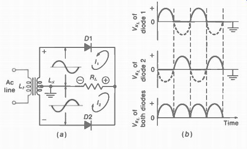
FIGURE 12-12 FULL-WAVE. CENTER TAP RECTIFIER. (a) CIRCUIT. /, AND I. SHOWN
IN DIRECTION OF ELECTRON FLOW. (b) WAVESHAPES WITHOUT FILTER.
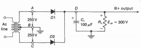
FIGURE 12-13 FULL-WAVE, CENTER TAP RECTIFIER CIRCUIT WITH FILTER CAPACITOR
C1.
In Fig. 12-13, the full-wave circuit is shown with a capacitor input filter. Each diode conducts only at the peak of the positive ac input to charge C1. The waveshape of the peak charging current for each diode is the same as shown in Fig. 12-9 for a half-wave rectifier. Since both diodes charge C1, however, a smaller filter capacitor can be used in a full-wave rectifier.
The dc output voltage in Fig. 12-13 is calculated as 1.2 x 250 = 300 V. This is a typical 6+ voltage for vacuum tube amplifiers in an ac receiver with a center-tapped power transformer. This circuit was commonly used with a dual diode vacuum tube rectifier such as the 5U4. With solid-state rectifiers now, though, it is preferable to use circuits that do not need a center tap. For vacuum tube rectifiers, bridge circuits and voltage doublers have the complications of extra heater connections, but this is eliminated with solid-state diodes.
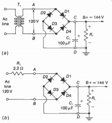
FIGURE 12-14 FULL-WAVE BRIDGE RECTIFIERS. (a) LINE ISOLATED WITH POWER TRANSFORMER.
(b) NO ISOLATION FROM POWER LINE.
12-7 Full-WaveBridge Rectifier
This circuit is a full-wave rectifier that does not need a center-tapped power transformer. As shown in Fig. 12-14, the entire ac input is used for dc output voltage. In a, T, is used as an isolation transformer. The turns ratio is 1:1, to supply the same 120-V ac input as the line-connected supply in b. If necessary, though, the power transformer can step up or step down the ac voltage. Note that the surge-limiting resistor R, in b takes the place of the transformer resistance in a.
The advantage of a bridge rectifier is that both half-cycles of the ac input are rectified, without a center-tap to provide opposite polarities. The disadvantage is that four diodes are necessary. This factor was inconvenient with vacuum tube rectifiers because of the heater connections. However, semiconductors do not have heaters. A small bridge rectifier unit with four diodes is shown in Fig. 12-15.
The details of conduction by the four diodes in the bridge are shown in Fig. 12-16. In brief, the operation of the bridge allows two diodes to conduct in series with the load R1 , on each half-cycle. The equivalent circuit in a shows that R _p is the center arm of the bridge.
The right side at point C is at a rectifier cathode, either for D1 or D4, for positive dc voltage output. The opposite end of R1 , at point D is chassis ground. The result is B+ voltage at the cathode side of R_L, with respect to ground.
When point B is negative in Fig. 12-16b, the cathode is negative and anode positive for D3 and D1, making these diodes conduct. The electron flow I_31 is from the bottom of L s, from cathode to anode in D3, through Rt, from cathode to anode in D1, and returning to point A at the top of L s. D2 and D4 are not shown in this diagram. They are effectively out of the circuit because of reverse bias with positive cathode voltage on D2 and negative voltage for the anode of D4.
On the next half-cycle when point A is negative in Fig. 12-16c, D2 and D4 conduct. The electron flow I_24 is from the top of L s, from cathode to anode in D2, through R_L, from cathode to anode in D4, and returning to point B at the bottom of L_s. Now Q1 and Q3 are out of the circuit because they are biased off with reverse voltage.
Note that I is in the same direction through R1 , for both half-cycles. The result is B+ voltage at the cathode side of R _p, with respect to ground. If all four diodes were reversed, the dc output voltage would be negative.
The ripple frequency of the full-wave bridge is 120 Hz because both half-cycles of the ac input produce dc output. Note that the filter capacitor C, in Fig. 12-14 has the same value of 100 as C, for the full-wave center-tap rectifier in Fig. 12-13. The dc output voltage in Fig. 12-14 is calculated as 1.2 x 120 = 144 V.
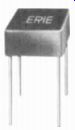
FIGURE 12-15 BRIDGE RECTIFIER WITH FOUR DIODES IN ONE UNIT. SIZE IS V2-IN.
SQUARE. ( ERIE TECHNOLOGICAL PRODUCTS INC.)
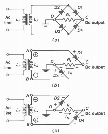
FIGURE 12-16 HOW THE BRIDGE RECTIFIER CONDUCTS ON OPPOSITE HALF-CYCLES OF
THE AC INPUT (a) THE LOAD R, IS IN THE CENTER ARM OF THE BRIDGE (b) WHEN POINT
A IS POSITIVE, 01 AND D3 CONDUCT THROUGH R, (c) WHEN POINT B IS POSITIVE, 04
AND D2 CONDUCT THROUGH R,
12-8 Voltage Doublers
By series combinations of half-wave diodes and their filter capacitors, the amount of dc output voltage can be doubled, tripled, or quadrupled.
Typical circuits are shown in Figs. 12-17 to 12-21. Even higher multiplication is possible, but the voltage regulation becomes worse and very large filter capacitors are necessary. In practical applications, the voltage doubler is often used for the B+ supply, especially the half wave line-connected supply shown in Fig. 12-17.
Voltage triplers and quadruplers can be used in the high-voltage supply for anode voltage on color picture tubes.
Hall-wave voltage doubler. See Fig. 12-17.
This circuit is also called a cascade doubler because the rectified output of D1 is used for input to D2. The two diodes conduct on opposite half-cycles. We can start with the negative half-cycle of the ac input that drives the cathode of D1 negative. Then this diode con ducts to charge C1. Note the polarity of the dc voltage across C. On the next half-cycle, when point A is positive, the C1 voltage is connected series-aiding with the ac input voltage. Then the input for D2 is doubled, with the anode positive for conduction. As D2 charges C2, the dc output voltage across C2 is doubled. R, is the surge-limiting resistor for both diodes.
This circuit is a half-wave rectifier be cause dc output across C2 is produced only on the positive half-cycle of the ac input when D2 conducts. The ripple frequency, then, is 60 Hz.
An important feature of this doubler is that one side of the ac input and dc output are common. For this reason, the half-wave doubler is generally used as a line-connected supply, without a power transformer. As shown in Fig. 12-17, the grounded side of the dc output is common to the neutral or grounded side of the ac input. The common connection reduces the problem of stray pickup of 60-Hz hum in the receiver.
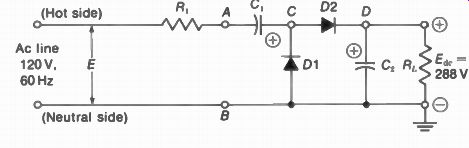
FIGURE 12-17 TYPICAL VOLTAGE DOUBLER. THIS TYPE IS A HALF WAVE OR CASCADE
DOUBLER CIRCUIT
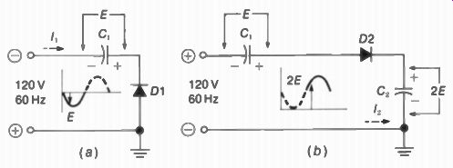
FIGURE 12-18 OPERATION OF HALF WAVE VOLTAGE DOUBLER. (a) CIRCUIT
FOR D1 CHARGING C1, WITHOUT D2 (b) CIRCUIT FOR D2 CHARGING C. WITHOUT D1.
Because the half-wave doubler is often used for the low-voltage supply, more details of its operation are illustrated in Fig. 12-18. In a, the circuit is shown for D1 alone. The other diode D2 is effectively out of the circuit because its anode is reverse-biased on this half-cycle when the ac input voltage is negative. The electron flow I_1 then charges C, with the positive side at the cathode of D1. This dc voltage has the same polarity on both half-cycles of the ac input.
In b, when the ac input voltage is positive, D2 conducts without D1. Note the series-aiding polarities, as the minus side of C, is at the positive side of the ac input. This connection is the same as series-aiding batteries. The effect, then, is to lift the ac input voltage to a higher level on the axis of the dc voltage across C. This effect is shown by the waveform in b.
The peak of the combined voltage for D2 is almost twice the peak of the ac input voltage alone. As a result, D2 charges C2 to double the dc output voltage of one half-wave rectifier alone. If we consider the value of E across C, in Fig. 12-18a as 1.2 x 120 = 144 V, then the doubled output across C2 in b is 2E = 288 V. Full-wave doubler. See Fig. 12-19. On the half cycle when point A is positive, D1 conducts to charge C1. On the next half-cycle D2 conducts to charge C2. The dc output voltage is taken across C1 and C2 in series. Therefore, the dc output is doubled. The ripple frequency is 120 Hz, since both half-cycles of the ac input produce dc output. The full-wave voltage doubler circuit is seldom used, however, because it does not have a common connection for ac input and dc output.
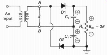
FIGURE 12-19 CIRCUIT OF FULL-WAVE VOLTAGE DOUBLER.
12-9 Voltage Triplers and Quadruplers
For a tripler, the voltage doubler is combined with a single half-wave rectifier. For a quadrupler, two doublers are connected in cascade.
Referring to the half-wave voltage tripler in Fig. 12-20, D1 and D2 form a cascade voltage doubler. Furthermore, the doubled voltage 2E across C2 is applied to D3 in series with Cc and the ac input voltage. On the half-cycle when point B is positive, the ac voltage across the AB terminals is series-aiding with the dc voltage 2E. As a result, conduction in D3 charges C„ to 3E, which is triple the input voltage.
For the half-wave voltage quadrupler in Fig. 12-21, D1 and D2 form one voltage doubler.
Also, D3 and D4 form a voltage doubler. C1 is the series capacitor for D3, corresponding to C1 for D1. The output is 4E because the input to D4 is the dc voltage 3E across C„ in series with the ac input voltage.
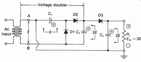
FIGURE 12-20 CIRCUIT OF HALF WAVE VOLTAGE TRIPLER
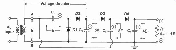
FIGURE 12-21 CIRCUIT OF HALF-WAVE VOLTAGE OUADRUPLER
12-10 Heater Circuits
For receivers that use tubes, the heaters can be connected either in series or in parallel. With a transformer to step down the ac line voltage from 120 to 6.3 V, the heaters are in parallel across the filament winding (Fig. 12-22). Then all the parallel heaters have the same 6.3-V rating, although the individual branch currents can be different. In the line-connected supply without a power transformer, all the heaters are connected in series to the ac power line (Fig. 12-23). Then the current is the same in all parts of the series string. Therefore, heaters with the same current rating must be used, although the individual heater voltages can be different.
The current is usually either 450 or 600 mA for series heater strings. All the series voltage drops add to equal the power-line voltage of 110 to 120 V. It is important to remember that when one heater is open, there cannot be any current in the entire series string.
Parallel heaters. In Fig. 12-22, one end of the filament winding L f is tied to chassis ground to Save wiring. The opposite end is the high side connecting to all the heaters in parallel. Each heater returns to L f by an individual ground connection. Note that the heater pins are usually 3 and 4, or 4 and 5 on the amplifier tubes. With parallel connections, when one heater is open, the other heaters are not affected.
Filament chokes. The 1-uH coil L1 in Fig. 12-22a is a few turns of thick wire to serve as a choke for rf or IF signals. With the rf bypass C, of 0.047 uF, L, and C, provide a decoupling filter to prevent feedback of signals between rf and IF amplifiers through the common heater line. The choke L1 has high reactance for the signal frequencies but practically none for the 60-Hz heater current. Therefore, the heaters are still effectively in parallel as shown in b. Such rf decoupling filters are also used in series heater circuits. Ferrite beads may be used instead of the rf choke.
Series heaters. In Fig. 12-23, all the heaters including the picture tube are in series across the power-line voltage of 110 to 120 V. The current is 450 mA in all these series heaters. The sum of the heater voltages here is 109 V. With the 6.8 V across R, 14, the total of all the IR drops then is 115.8 V, approximately equal to the power-line voltage. The high-voltage rectifier is not in the series string, as it receives filament power from the horizontal output transformer.
Color receivers also have series heaters, but the color picture tube often has its own 6.3-V filament transformer. This heater usually has a dc bias voltage added to raise its potential close to the cathode voltage. The purpose is to minimize internal arcing.
Center-tapped heater. Some tubes have the heater in two sections that can be wired either in series for 12.6 V or in parallel for 6.3 V. Examples of such tubes with three heater pins are the 12AU7, 12AT7, and 12BY7.
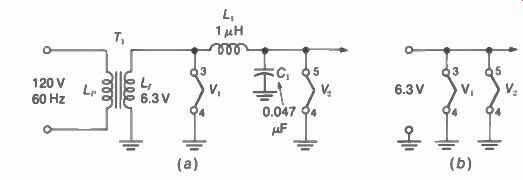
FIGURE 12-22 PARALLEL CONNECTIONS FOR 6.3-V HEATERS. (a) WITH RF DECOUPLING
FILTER L,C,. (b) EQUIVALENT CIRCUIT FOR 60 Hz.
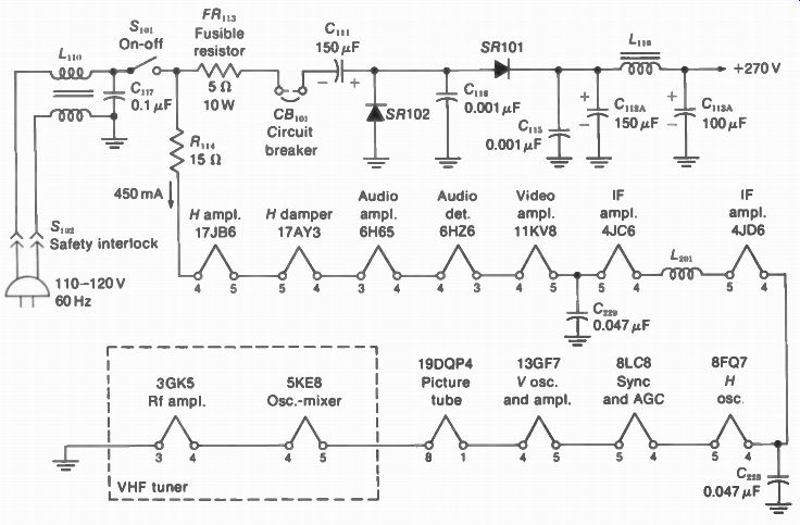
FIGURE 12-23 SERIES HEATER STRING WITH CASCADE VOLTAGE DOUBLER FOR LOW VOLTAGE
SUPPLY. (RCA MONOCHROME CHASSIS KCS 142)
Controlled warmup time. All the tubes in a series string should reach operating tempera ture at the same time. Otherwise, the cold heaters have too little resistance, allowing too much voltage across the hot tubes just after the set is turned on. The uneven warmup time can cause repeated troubles of a burned-out heater in the series string. This used to be a common problem with series heaters. However, now tubes for series strings are designed to reach 80 percent of rated heater voltage in 11 s, with specified test conditions. In actual operation, typical warmup time for a series string without a thermistor is about 50 s for a full raster. The warmup is much shorter for parallel heaters.
Some heater strings have a thermistor in series to limit the current until the tubes become hot. A thermistor has a negative temperature co efficient, meaning its resistance decreases with heat. Typical values are 100 ohms for the cold resistance, decreasing to 10 ohm for the hot resistance.
The thermistor for the heater string is also called a tube saver. With a thermistor, the warmup time for the receiver can be as long as 2 min.
Order of series heater connections. All the series heaters have the same current, but a point closer to the grounded end of the string has less potential difference to chassis ground for 60-Hz voltage. Therefore, less hum voltage can be coupled into the signal circuits by heater cathode leakage in the tube. This factor is why the tubes in the VHF tuner are last in the string, while the horizontal deflection amplifier and damper tubes are first, as in Fig. 12-23.
It is important to note the difference between measuring the 60-Hz ac voltage across the heater pins or measuring from one pin to chassis ground. For instance, in Fig. 12-23 the ac voltage across the heater pins 4 and 5 of the 17JB6 is 17 V. However, from pin 4 to ground, you measure 109 V of the ac line voltage. At pin 4 to ground, the ac voltage is 17 V less, or 92 V. 12-11 Filter Circuits
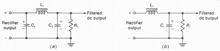
FIGURE 12-24 FILTER CIRCUITS. (a) CAPACITOR INPUT. (b) CHOKE INPUT.
FIGURE 12-25 CIRCUIT FOR ACTIVE FILTER. SEE TEXT FOR EXPLANATION.
The function of the filter is to remove the ac ripple. The two basic types for power supplies are the capacitor input filter in Fig. 12-24a and the choke input filter in b. The difference is that C1 in a can be charged by the rectifier current without the series inductance of the choke L1. C1 is the input filter capacitor at the rectifier, while C2 is the output filter capacitor across Rt. Because of the peak charging current for C2 the capacitor input filter produces more dc output voltage than the choke input filter. There is also less ripple voltage, for moderate values of load current.
The choke input filter has better voltage regulation. Also, the amount of ac ripple voltage does not increase with the load current. The capacitor input filter is generally used in receivers, however, because of its higher output voltage.
Typical values of C are 50 to 2,000 uF while L is 2 to 10 H. The dc resistance is 250 for a 5-H choke rated at 200 mA. A filter resistor of 100 to 1,000 ohm can be used instead of the choke in some power supplies with relatively small values of load current. Large filter capacitances of 500 to 2,000 µF are needed in transistorized receivers because of more dc load current and smaller dc voltages, compared with vacuum tubes.
Percent ripple. This is the ratio of the rms value of the ac ripple voltage to the dc output voltage, times 100 for the percentage. As an example, with 1.4 V for the ac ripple and 140-V dc output, 1.4 % ripple = x 100 = 1% 140
This value is typical at the input filter capacitor.
The output filter capacitor C2 has even less ripple in the B+ voltage for the load.
Active filter. A transistor can be used as an electronic filter, as shown in Fig. 12-25. Note that Q1 is effectively in series with the power supply and the load, corresponding to a series choke. The electronic filter removes ripple variations in the load current because the transistor has relatively constant current in the collector output circuit. In the base circuit, the ripple is easy to filter by C, because of the small value of current. Forward bias for the base is provided by R, from the positive collector voltage. The diode D1 clamps the bias at approximately 0.7 V for constant saturation current in the collector circuit. In the output circuit, additional filtering is provided by the pi-type filter consisting of C2, R2, and C3.
12-12 Voltage Regulators
Regulation in a power supply means keeping the dc voltage output constant with variations either in dc load current or in ac input voltage. As one example, a voltage regulator is generally used for the anode voltage of a color picture tube.
Constant high voltage is needed to maintain focus and convergence with changes in brightness. In the low-voltage supply of solid-state receivers, regulation is important in order to maintain constant raster size.
In general, voltage regulation is useful because it also improves the filtering of ac ripple and reduces the ac output impedance of the power supply. Low impedance minimizes the coupling between amplifier stages through the common B+ line.
The types of voltage regulator circuits in television receivers range from the relatively simple zener diode to more complicated feed back circuits. The following list illustrates the common methods of regulation.
1. Zener diode. Remember that with reverse breakdown, the voltage across the zener diode is constant for a wide range of current values through the diode. Zener regulators are commonly used in voltage ratings of 3 to 180 V.
2. Voltage-regulating power transformer.
This special transformer in the low-voltage supply regulates the ac line voltage input.
Regulation is accomplished by using saturation of the core to limit increases and by resonance in the secondary to limit de creases. An external 3.5-µF oil-filled capacitor tunes the secondary winding to 60 Hz.
3. Feedback regulators. In this method, a sample of the output is fed back to a control stage, which can then regulate the circuit for constant output. The current in a tube or transistor can be controlled, as a variable resistance, by varying the bias. A shunt regulator is in parallel with the output circuit to bypass more current or less current around the load. A series regulator provides a variable voltage drop in series with the output voltage.
Zener-diode regulator. See Fig. 12-26. Note the schematic symbol for the zener diode Z1.
Reverse bias is used with positive voltage at the cathode. This zener diode is rated for 12-V breakdown voltage, with a maximum diode current of 150 mA and 10-W power dissipation.
Smaller units have a power rating of 400 mW or 1 W. The series regulating resistance R, has the function of providing a voltage drop that varies with the load current. However, there must be at least 12 V across the diode to provide current through Z1 so that it can operate in its break down mode.
The 6BK4 shunt regulator. See Fig. 12-27.
This circuit is used for regulating the high voltage supply in most color receivers with vacuum tubes. The shunt current through the 66K4 regulator V3 and the load current, which is the beam current in the picture tube, together remain constant as a total current. With constant load current in the HV rectifier, its output of 25 kV remains constant.
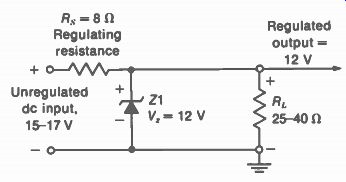
FIGURE 12-26 ZENER-DIODE VOLTAGE REGULATOR CIRCUIT. NOTE 12 V ACROSS Z1 IS
REVERSE BIAS.
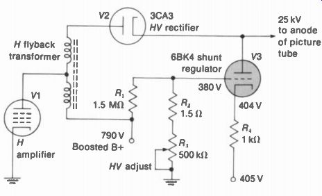
FIGURE 12-27 THE 6BK4 HIGH-VOLTAGE SHUNT REGULATOR CIRCUIT.
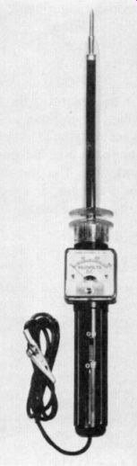
FIGURE 12-28 VOLTMETER FOR MEASURING CRT HIGH VOLTAGE ON ANODE. LENGTH IS
15 IN. MULTIPLIER RESISTANCE IN PROBE IS 600 M-O. ( POMONA ELECTRONICS)
The regulation of the 6BK4 results from varying its bias. In Fig. 12-27, the grid-cathode voltage is 380 - 404 = - 24 V. Note that the 380V at the grid is obtained from the boosted B+ of 790 V in the horizontal output circuit. This voltage depends on the load for the horizontal amplifier V1.
Suppose that the beam current in the picture tube increases with more brightness.
This factor will tend to decrease the high voltage. Then the boosted B+ voltage decreases slightly because of the added load current for V1. As a result, assume that the positive grid voltage for V3 decreases by 5 V. This means the grid-cathode bias is 5V more negative. The result is less current in the 6BK4 regulator. For the opposite case, less beam current for the load allows more beam current in the shunt regulator circuit. Together, the load current for the anode of the picture tube and the shunt regulator current remain at a constant value for the total current supplied by the HV rectifier.
The high-voltage adjustment R3 in Fig. 12-27 is set as follows:
1. Turn brightness and contrast controls to minimum for a black screen and maximum high voltage.
2. Connect high-voltage probe (Fig. 12-28) to measure anode voltage.
3. Set the variable resistance R3 for the specified anode voltage, which is usually 25 kV for a 21-in, color picture tube.
With this adjustment, the regulator should be drawing approximately 1-mA cathode current.
Then the IR drop would be 1V across the 1-k-ohm cathode resistance R4 in Fig. 12-27.
Feedback circuit with series regulator transistor. See Fig. 12-29. Q1 is the series regulator that provides output to the load. Q2 is the driver to control the bias on Q1. The driver has two input voltages. One is a reference of 11.2 V stabilized by the zener diode in its emitter circuit. The other is the sensing voltage of approximately 11.8 V, from a tap on the R1R2R3 voltage divider across the output.
The amount of conduction in the driver Q2 determines the bias on the regulator Q1.
Furthermore, the driver Q2 compares the reference of 11.2 V in the emitter to the sample voltage from R2, which is approximately one-tenth the output, applied to the base. Any difference is amplified to change the bias and conduction for the series regulator Q1. The adjustable resistor R2 for the driver Q1 is set for exactly 115 V at the output of the series regulator Q1.
12-13 Low-Voltage Supply with Series Regulator Circuit
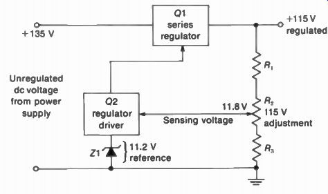
FIGURE 12-29 SERIES REGULATOR FOR LOW-VOLTAGE POWER SUPPLY
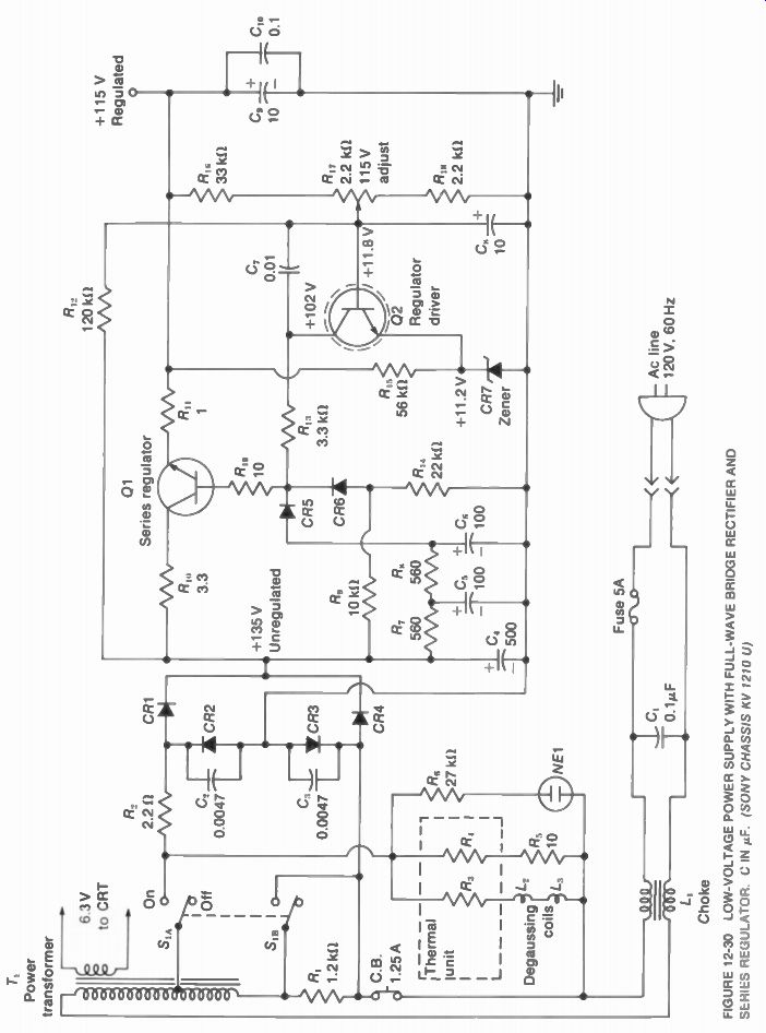
FIGURE 12-30
This circuit for a solid-state color television receiver is shown in Fig. 12-30. The rectifier uses a full-wave bridge, with CR1, CR2, CR3, and CR4. R2 is a surge-protective resistance of 2.2-ohm. C2 and C3 are hash suppressors for the diodes. The B+ supply is line-connected, al though the autotransformer T, supplies an isolated 6.3 V for the heater of the picture tube. In the ac input, a 5-A fuse and 1.25-A circuit breaker provide protection against overload. L, and C, are hash filters for the power line. The degaussing coils L2 and L_3 are fed ac power from the line, through the thermal unit consisting of R3 and R4,. The on-off S, is a double-pole switch, connects the ac line to the bridge rectifier for B+ voltage. However, S1B only has the function of shorting R, in series with the line. When the receiver is off, S1B is open. Then R1 is in the circuit to decrease the line current for reduced heater power on the picture tube. When the receiver is on, S1B is closed to short R,.
The result is full heater power for the picture tube and approximately 110-V ac input for the bridge rectifier with S, , closed. The neon bulb NE1 indicates that voltage is applied to the B+ circuit.
The bridge rectifier produces 135 V, at the 500-µF input filter capacitor C.,. The two-section filter consisting of R, and R„ with C4, C5, and C„ removes the 120-Hz ripple. In addition, the output of 135 V goes to the regulator circuit consisting of Q1 and Q2. This is the same series regulator illustrated in Fig. 12-29. The dc output from the emitter of Q1 is a well regulated +115 V. R17 is adjusted to produce this output voltage. Additional filtering in the output is provided by the 10-µF C, and 0.1- uF C,„ in parallel. The purpose of the small paper capacitor is to provide low reactance for rf signal frequencies, across the self inductance of a large electrolytic capacitor.
----------

TABLE 12-1 TROUBLES IN THE B+ VOLTAGE NO 8+ VOLTAGE LOW 8+ VOLTAGE
No ac line voltage
Open diode in half-wave rectifier
Open fuse or circuit breaker
Open in series filter R or L
Short in shunt filter capacitor
Low ac line voltage
Open diode in doubler or bridge circuit
Leakage in diode rectifier
High resistance in series filter R or L
Open in shunt filter capacitor
-------------
12-14 Troubles in the Low-Voltage Supply
A trouble here is common to all sections of the receiver because it produces multiple effects.
Two common indications are:
(1) no brightness and no sound because of no B+ voltage, and (2) a small raster because of low B+ voltage. Typical troubles are listed in Table 12-1.
No B+ voltage. The receiver will be dead, without any brightness or sound, although the heaters can light. Remember that the B+ line usually has a protective fuse or circuit breaker that may be open. Also, in many receivers the B+ line is opened when the yoke plug is out of its socket. Troubles that can cause no 8+ voltage include an open diode in a half-wave rectifier circuit, an open filter choke or resistor, and a shorted filter capacitor.
Low B+ voltage. As an example, if the B + voltage is reduced 25 percent, the raster will be about 10 percent smaller. The focus may also be affected. The sound will probably be normal, as the volume is not reduced until the B+ is down about 40 percent. The same effects are produced by a low value of line voltage for the ac input.
A common cause of low B+ voltage is an open input filter capacitor. Furthermore, a diode can be open in a doubler or a bridge rectifier to cause reduced B+ voltage, instead of no output. It should be noted that when one side of a full-wave bridge is open, the ripple frequency is 60 instead of 120 Hz.
Open in series heater line. An open in one heater means no current in the entire series string. The full ac line voltage is across the open heater because its resistance is infinitely high. If you check each heater with an ac voltmeter, the open heater has 120-V. If you use an ohmmeter with power off, the open heater reads infinite ohms. Start with the tubes for the power stages, such as audio output, vertical output, horizontal output, and damper. These tubes cause the most trouble because they generate the most heat.
Open filter capacitors. What happens, usually, is that the electrolyte dries out. Then the capacitor becomes open or practically open with reduced capacitance. With an open input filter capacitor, the result is reduced B+ voltage and excessive hum. When the output filter capacitor is open, the result is poor regulation of the B+ voltage for the load.
Effects of poor regulation in B+ voltage. The circuits that draw the most load current from the B+ supply are the deflection amplifiers and audio output stage. When the B+ voltage varies with the load current in the audio amplifier, the result can be sound bars in the picture. These sound bars disappear when you turn down the volume. When the B+ voltage varies with the load current in the vertical amplifier, the result can be vertical shading in the picture. Finally, when the amount of B+ voltage changes, the size of the raster can increase or decrease, especially with changes in the ac line voltage.
FIGURE 12-31 EFFECTS OF HUM (a) 60-Hz HUM BARS IN PICTURE. (b) 60-Hz HUM BEND
IN RASTER
----------------

TABLE 12-2 HUM TROUBLES
HUM
60 Hz | 120 Hz
In video signal
One pair of horizontal black-and-white bars
Two pairs of horizontal black-and-white bars
In horizontal scanning
One cycle of sine-wave bend at sides of raster
Two cycles of sine-wave bend at sides of raster
In horizontal sync
One cycle of sine-wave bend at sides of picture
Two cycles of sine-wave bend at sides of picture
In vertical sync
Poor vertical synchronization in picture
Poor vertical synchrorization in picture
In vertical scanning
Nonlinear vertical scanning
Nonlinear vertical scanning
---------------
12-15 Hum in the B+ Voltage
Hum is excessive ac ripple in the dc output of the low-voltage power supply. The cause is poor filtering, usually as a result of open filter capacitors. The ripple frequency is 60 Hz in a half-wave rectifier or 120 Hz in a full-wave circuit. In the sound, the ac ripple produces hum. On the screen of the picture tube, the hum car cause horizontal black-and-white hum bars or bend at the sides. See Fig. 12-31. Typical hum troubles are summarized in Table 12-2.
For all these hum effects, remember that the vertical scanning frequency for color television is exactly 59.94 Hz, not 60 Hz. As a result, the 60-Hz hum patterns do not stay still. Hum bars drift slowly up the picture. Also, hum bend at the sides crawls upward on the screen.
Hum in the video signal. Hum voltage can be amplified by the video section supplying signal for the picture tube. The result is black-and white bars across the screen, as shown in Fig. 12-31a. One pair of bars is shown here for 60-Hz hum. With 120-Hz ripple, the result is two pairs of hum bars.
Hum in the horizontal scanning. The result is sine-wave bend at the sides of the raster (Fig. 12-31b). One cycle of bend is produced by 60 Hz; two cycles show 120 Hz. This bend is in the raster and in the picture.
Hum in the horizontal sync. The result is sine wave bend in the picture but not in the raster. If you remove the picture, the raster will have straight sides.
Hum in the vertical sync. This trouble makes it difficult to lock in the picture vertically. One specific effect is a picture halfway out of position, as the vertical oscillator is synchronized by the hum voltage instead of vertical sync. Then the black vertical blanking bar is across the middle, while the top and bottom of the picture are reversed.
Hum in the vertical scanning. The result is nonlinearity from top to bottom of the picture.
The reason is that the sine-wave ac ripple combined with the sawtooth sweep results in nonlinear vertical scanning.
12-16 Flyback High-Voltage Supply
Practically all television receivers use this circuit because the required high-voltage ac input for the high-voltage rectifier is produced by the fast drop of current in the horizontal output transformer during horizontal retrace. Details of the horizontal output circuit are explained in Section 22, but the basic requirements for flyback high voltage are illustrated in Fig. 12-32. T1 is an autotransformer for the horizontal output. This is called the flyback transformer.
Terminals 1 and 2 on T1 supply output to the horizontal coils in the deflection yoke for horizontal scanning. Terminals 1 and 3 serve as the primary for the horizontal deflection amplifier. This can be a tube or a transistor. Terminal 4 has the stepped-up voltage for the high-voltage rectifier. Figure 12-33 shows a typical flyback transformer.
When the output current drops to zero for horizontal flyback, the fast change in current produces a high value of induced voltage at terminal 4 of T1 for the high-voltage rectifier. The voltage peak has positive polarity to oppose the decrease in current. With the rectifier plate positive, it conducts to charge the filter capacitance C,. This is the anode capacitance of the picture tube. The result is 18-kV positive dc voltage at the directly heated cathode of the high-voltage rectifier.
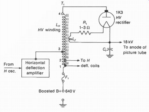
FIGURE 12-32 BASIC CIRCUIT OF FLYBACK HIGH-VOLTAGE SUPPLY
The flyback transformer and rectifier are generally in a separate metal cage. In addition to protection against shock, the enclosure is a dust cover and shield against x-rays. When the receiver has a fuse such as F, for the horizontal output circuit, it is generally in or near the cage.
An open fuse for the horizontal amplifier can be a simple cause for the trouble of no high voltage and no brightness, while the sound is normal. A practical point to remember is that in some receivers, the high-voltage output is disconnected when the cage cover is off.
High-voltage rectifiers. Tubes commonly used for anode voltage of 10 to 20 kV for mono chrome picture tubes are the 1B3, 1G3, and 1K3.
The top cap is the plate on these tubes. All have essentially the same ratings of 30,000-V peak in verse voltage, heater voltage of 1.25 V at 0.2 A, and dc output of 0.5 mA or less for the load current. Because of the small heater power, the filament voltage can be taken from the horizontal output transformer by the winding L1 in Fig. 12-32. This is only one turn of heavy wire wrapped on the core of the transformer. A separate filament transformer would require enough insulation to withstand the high dc voltage at the rectifier filament without arcing to chassis ground. Note that R1 drops the heater voltage to 1.25 V. This may be a carbon resistor, or resistance wire can be used.
For color picture tubes, a larger tube is needed for the high-voltage rectifier because of more load current. Tubes commonly used are the 3A2 and 3CA3. The rated heater voltage is 3.15 V at 0.22 A, with a maximum load current of 2 mA. For either monochrome or color picture tubes, a silicon-diode rectifier can be used.
These are special high-voltage diodes with the required rating for peak inverse voltage. See Fig. 12-34.
High voltage for focusing. Color picture tubes with high-voltage electrostatic focusing generally require 5 to 7 kV for the focus grid. This voltage is taken from the horizontal output circuit.
Either a separate rectifier can be used as in Fig. 12-35, or a tap on the high-voltage supply can provide the focusing voltage, as in Fig. 12-36.
In Fig. 12-35, the silicon diode X1 is the focus rectifier. Tubes also used for this function are the 1V2 and 1X2. These high-voltage rectifiers do not have a top cap for the anode and are smaller than the 1K3.
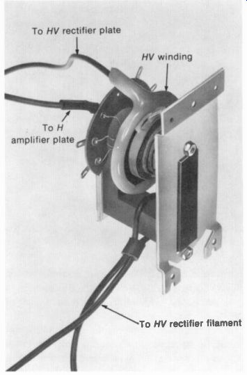
FIGURE 12-33 HORIZONTAL FLYBACK TRANSFORMER.
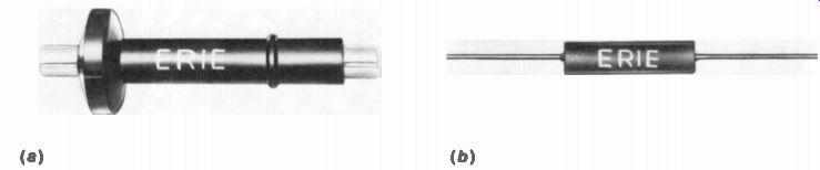
FIGURE 12-34 SILICON HIGH-VOLTAGE RECTIFIERS FOR COLOR RECEIVERS. (a) 30-
TO 45-kV RATING FOR ANODE VOLTAGE OF CRT. LENGTH IS 4 IN. THIN END AT RIGHT
IS CATHODE SIDE. (b) 5- TO 10-kV RATING FOR FOCUS VOLTAGE. LENGTH IS 2 IN.
( ERIE TECHNOLOGICAL PRODUCTS, INC.)
In Fig. 12-36 the high-voltage rectifier is a solid-state tripler circuit with the silicon diodes, capacitors, and resistors all in one unit. A tap at the output of the first rectifier supplies 7.7 kV to the focus control circuit.
Blooming. This term describes a picture that increases in size, with defocusing in white areas, as the brightness is increased. The blooming results from a sharp decrease in the amount of anode voltage when the beam current is increased to turn up the brightness. It should be noted that the scanning current produces more deflection, and the raster becomes bigger, with less high voltage. A common cause of blooming is a weak high-voltage rectifier, which has excessive internal resistance. Another reason is too little bias on the picture tube. Color receivers generally have a brightness-limiter circuit to prevent blooming, by limiting the bias set with the brightness control.
Breathing. This term refers to blooming at a slow, regular rate. The size of both the raster and picture changes with variations in the high voltage. The cause is usually trouble in the high voltage regulation.
Corona and arcing. A point at high potential can ionize the surrounding air to produce a visible corona effect, which is light blue in color.
The corona causes loss of power and eventual insulation breakdown with arcing. In addition, precipitation of ionized dust particles is a result of the corona.
To minimize corona, it is important to eliminate sharp edges in the wiring. Also, all soldered joints must be smooth and round. Thick wires have less corona, as the voltage gradient of the conductor surface to the surrounding air is reduced. The high-voltage rectifier socket often has a thick metal ring, called a corona ring, for the cathode connection to the dc high-voltage output.
Corona and arcing in the high-voltage supply can produce streaks in the picture. To recognize these effects, arcing can usually be heard as a snapping noise, while corona produces a sizzling sound. Often you can see the corona or arcing by looking into the high-voltage cage. It can be helpful to note that do arcing is white, but the corona effect from ac voltage looks blue.
All high-voltage connections must be well separated from the chassis to eliminate arcing.
If we take the voltage breakdown rating of air at 20 kV/in., the high voltage of 25 kV can jump a gap of 1 1 /4 in.
Brightness troubles. The brightness on the screen of the picture tube depends directly on the amount of high voltage. No high voltage means no brightness. Insufficient high voltage causes low brightness, usually with poor focus.
Remember that the horizontal scanning circuits must be operating to produce the flyback high voltage. Also, trouble in the regulator can cause no high voltage or reduced voltage with poor focus.
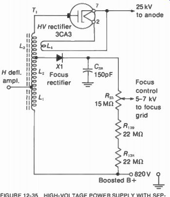
FIGURE 12-35 HIGH-VOLTAGE POWER SUPPLY WITH SEP ARATE FOCUS RECTIFIER. (ZENITH
COLOR CHASSIS 23XC38)
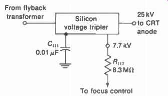
FIGURE 12-36 SILICON VOLTAGE TRIPLER FOR ANODE VOLTAGE, WITH TAP FOR FOCUS
VOLTAGE (RCA COLOR CHASSIS CTC 58)
12-17 Fuses and Circuit Breakers
Typical examples are shown in Fig. 12-37. The function of these safety devices is to open the circuit when a trouble causes excessive current.
Sometimes the cause is a temporary surge of line voltage or circuit overload. However, when a fuse is replaced and blows again, the trouble is probably a short circuit that must be corrected.
Do not use a fuse higher than the specified current rating. The purpose is to have the fuse open before the series components can burn out with too much current. It is the current rating of the fuse that provides the protection.
Fuses with just a straight wire link inside are fast-acting. They will blow in less than 0.3 s with a 400 percent overload. A "slow-blow" fuse has a coiled construction. The purpose is to prevent the fuse from blowing with just a temporary current surge. As an example, such a 1-A fuse will hold a 400 percent overload up to 2s.
Typical fuses are shown in Fig. 12-37a.
A circuit breaker (Fig. 12-37b) has a manual reset button to close the contacts after it has been tripped open by an overload. A bimetallic switch is used that opens with too much heat from excessive current. A 1-A circuit breaker will trip open with an overload current of 1.75 A in about 10s, as typical values.
The effect of an open fuse or circuit breaker depends on the circuit. A circuit breaker is usually in the line for B+ voltage, without the heaters. Therefore, an open causes no raster and no sound, but the heaters light. An open fuse in the main line to the ac input results in no B+ voltage and no heater power. This fuse is usually rated at 2 to 5 A. A fuse rated 1 to 2 A or less is usually just for the B+ voltage.
Remember that an open fuse in the horizontal output circuit causes no high voltage and no brightness, but the sound is normal.
Testing fuses with an ohmmeter. A good fuse reads 0 fl, showing continuity through the wire link. A blown fuse reads infinite ohms, showing an open circuit because the wire link is broken.
The power must be off, or the fuse removed from the circuit, to check with an ohmmeter.
Testing fuses with a voltmeter. It is important to realize that the test is different with power on.
Remember that a fuse is just a short piece of wire, with practically no IR drop. This applies whether the fuse is in an ac circuit or dc circuit.
When you measure between both ends of a good fuse, the voltage should be zero across the fuse.
With an open fuse, however, the voltmeter will read full voltage across the open circuit. The reason is that the high resistance of the volt meter takes the place of the fuse.
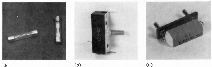
FIGURE 12-37 FUSES AND CIRCUIT BREAKERS. LENGTH ABOUT 1.5 IN. (a) GLASS CAR
TRIDGE FUSES. (b) CIRCUIT BREAKER WITH RESET BUTTON. (c) FUSIBLE RESISTOR.
If you measure the voltage from one end of the fuse to chassis ground, and then from the other end to chassis, the two readings should be exactly the same. A good fuse is practically a short circuit, and the voltage to chassis ground cannot be different at the two ends. With an open fuse, however, one end will read the full voltage to chassis ground while the other end reads 0 V. The reason is that one end is connected to the source of power but the other end is disconnected because of the open fuse.
Wire links. Heater circuits often have just a 1 to 2-in, length of thin, bare wire as the fuse. This type of wire fuse is usually soldered between two posts of a terminal strip in the chassis. A 2-in. length of No. 24 gage wire, as an example, can hold a current of 450 mA. Excessive current caused by a short circuit will burn open the wire fuse link. To replace it, just solder back another link, using the same gage wire.
Fusible resistors. These are wire-wound resistors used as a combination fuse and surge-limiting resistor for a silicon diode. A fusible resistor is often used in a line-connected supply without a power transformer, connected in series with the ac input for the diode, but not in the heater line. Typical resistance values are 3 to 10 as a surge-limiting resistor for the rectifier. The current rating is about 1 A as a fuse to protect the components in the B+ circuit. When the fuse opens, there is no 8+ voltage, but the heaters light. The fusible resistor usually has plug-in connectors, so that it can easily be replaced, as in Fig. 12-37c.
SUMMARY
The main characteristics of rectifier circuits are summarized in Table 12-3, for 60-Hz single-phase input from the ac power line. The ripple frequency is 60 Hz for a half wave rectifier or 120 Hz for a full-wave rectifier. The function of the filter is to remove the ac ripple from the dc output voltage. The function of a regulator is to keep the dc output voltage constant with a change in the amount of load current.
Self-Examination (Answers at back of guide)
Match the numbered statements at the left with the letters at the right.
1. Requires four diodes.
2. Maintains constant output voltage.
3. Reduces rf interference.
4. Keeps heaters warm when set is off.
5. Allows current in one direction.
6. Ratio of ripple to dc voltage.
Open heater in series string.
Surge-protective resistor.
Connected to one side of ac power line.
5 kV.
Flyback high-voltage supply.
Low B+ voltage.
7. Isolates set from ac power line.
8. Hot chassis.
9. Limits diode current.
10. Anode voltage for picture tube.
11. No raster and no sound.
12. Ripple frequency of 120 Hz.
13. Small raster.
14. Secondary winding not isolated.
15. Zero resistance.
16. Open filter capacitors.
17. Shunt regulator tube.
18. Focus voltage for color picture tube.
19. Manual reset button.
20. Fuse in ac power line.
(9)
(r)
(s)
(t)
Full-wave rectifier.
Hum.
Instant-on operation.
6BK4.
Bridge rectifier.
4 A. Good fuse.
Zener diode.
Hash filter.
Power transformer with separate secondary.
Circuit breaker.
Percent ripple.
Silicon-diode rectifier.
Autotransformer.
TABLE 12-3 RECTIFIER CIRCUITS
*Normal dc output voltage with typical load and capacitor input filter. E is rms value of ac input.
Minimum dc working voltage for peak dc output without load.
Essay Questions
1. Define the following terms: autotransformer; isolation transformer; line-connected, line-isolated, and ac-dc power supply.
2. Give the function of the following components in a power supply: power transformer, silicon diode, 10-H series choke, and 100-1iF shunt capacitor.
3. With 60-Hz input, give the ripple frequency for each of the following rectifier circuits: half-wave diode, full-wave center-tap; full-wave bridge; cascade doubler; and full-wave doubler.
4. Give two comparisons between a capacitor input filter and choke input filter.
5. What is the purpose of a voltage regulator?
6. Give one advantage and one disadvantage of series heaters, compared with parallel heaters.
7. Describe briefly how "instant-on" operation can be provided for a receiver with series heaters.
8. Why is there no brightness and no sound with an open heater in a series string?
9. Why is no brightness the result when: (a) high-voltage rectifier does not operate; (b) horizontal oscillator does not operate?
10. Give two effects of hum in the television receiver, as it shows on the screen of the picture tube. How do you distinguish between 60 and 120 Hz?
11. What is meant by "blooming" in the picture?
12. Describe briefly two insulation problems in a high-voltage supply.
13. Give two functions of the fusible resistor in a line-connected power supply.
14. How does the high-voltage rectifier obtain its heater voltage?
15. Referring to Fig. 12-29, how is R1 adjusted?
16. Referring to Fig. 12-27, how is R1 adjusted?
17. Give two ways in which a zener diode is different from a conventional diode rectifier.
18. Assume that a solid-state receiver rectifies the horizontal scan voltage for the low-voltage supply, in addition to the high-voltage supply for anode voltage on the picture tube. What will be the effects when the horizontal oscillator does not operate?
19. Draw the schematic diagram of a line-connected low-voltage power supply with a half-wave diode rectifier and series heaters. Show a pi-r-type filter and indicate the dc output voltage.
20. Draw the schematic diagram for a full-wave bridge rectifier with a 1:1 power transformer. Show a pi-r-type filter and indicate the dc output voltage.
21. Draw the schematic diagram for a line-connected voltage doubler, with pi-r-type filter, and give dc output voltage.
22. Compare a good fuse and open fuse for (a) resistance and (b) voltage.
23. Refer to the half-wave rectifier circuit in Fig. 12-11. Give the function for R1, C1, CR1, C2, C3A , L 2, and R2.
24. Refer to the voltage doubler circuit in Fig. 12-23. Give the function for R114 , C111 , L110, CB101, SR101, and SR102.
Problems
1. A series string totals 90 V with 600 mA in all the heaters. (a) What size voltage dropping resistor is needed with 120-V input? (b) How much power is dissipated in this R?
2. Refer to the series heater string in Fig. 12-23. List the ac voltages to ground at each tube, starting with pin 4 of the 17JB6.
3. Refer to the B + circuit in Fig. 12-23. If the dc load current is 160 mA and the resistance of L110 is 140 ohm, how much is the dc voltage at the input filter capacitor C112A?
4. The current through a 90-mH L drops from 400 mA to 0 in 8 ps. Calculate the induced voltage. [Hint: e = AO.]
5. Show how to connect the components in Fig. 12-38 in a cascade voltage doubler
FIGURE 12-38 FOR PROBLEM 5.