
As shown in Fig. 13-1, the video section amplifies the output from the video detector.
With signal of 2 V, peak to peak, one or two video amplifier stages can provide output of 100 V to the cathode of the picture tube for good contrast. Typical video signal for the picture tube is shown in Fig. 13-2. In color receivers, the video section amplifies the luminance (Y) signal, with essentially the same requirements as in monochrome receivers. The video amplifier is often dc-coupled from the video detector to the picture tube, in order to preserve the dc component for correct brightness, as explained in the next SECTION. Here, we analyze the problems of amplifying the ac video signal with frequency components from 30 Hz to 3.2 MHz, approximately. The main features of the video signal and video amplifiers are explained in the following topics:
13-1 Requirements of the video amplifier
13-2 Polarity of the video signal
13-3 Amplifying the video signal
13-4 Manual contrast control
13-5 Video frequencies
13-6 Frequency distortion
13-7 Phase distortion
13-8 High-frequency response of the video amplifier
13-9 Low-frequency response of the video amplifier
13-10 Video amplifier circuits
13-11 The video detector stage
13-12 Luminance video amplifier in color receivers
13-13 Functions of the composite video signal
13-14 The 4.5-MHz sound trap
FIGURE 13-1 THE VIDEO SIGNAL COUPLED TO THE CATHODE-GRID CIRCUIT OF THE PICTURE
TUBE REPRODUCES THE PICTURE INFORMATION ON THE RASTER.
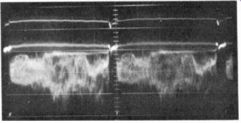
FIGURE 13-2 OSCILLOSCOPE PHOTO OF VIDEO SIGNAL VOLTAGE AT CATHODE OF PICTURE
TUBE. AMPLITUDE IS 100 V p-p.
13-1 Requirements of the Video Amplifier
The circuit is basically an RC-coupled stage, as shown in Fig. 13-3, operating class A for minimum distortion. In a, the 6.8-k ohm R_L is the plate load resistor with a 0.1-uF coupling capacitor. Similarly in b, the common-emitter amplifier has 6.8 k-O for R_L , and 0.1 uF for Cc,.. The RC values are the same here because both stages are considered as video output stages driving the picture tube. The contrast control varies the gain and the amount of video signal.
In a, the cathode resistance is varied, or the emitter resistance is varied in b.
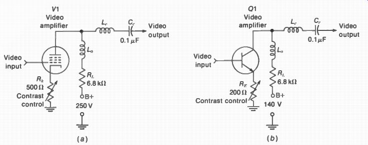
FIGURE 13-3 VIDEO AMPLIFIER CIRCUITS (a) PENTODE TUBE (b) CE TRANSISTOR STAGE.
FIGURE 13-4 VIDEO SIGNAL VARYING THE GRID VOLTAGE OF PICTURE TUBE
The peaking coils L o and L,. in the output circuit are small inductances of 100 to 250 uH that resonate with the stray capacitances to boost the response for high video frequencies.
The transmitted video signal includes frequencies up to 4 MHz, for horizontal detail. However, most receivers limit the video bandwidth to 3.2 MHz. The purpose is to minimize interference with the 3.58-MHz chrominance signal.
Video signal and picture reproduction. The function of the video signal is to vary the amount of beam current in the picture tube.
This intensity modulation reproduces the light or shade of the picture elements. Figure 13-4 shows how the input video signal voltage for one line, impressed between grid and cathode of the picture tube, results in reproduction of the picture elements for that line. This operating characteristic, or transfer curve, is for the picture tube, not for the video amplifier.
The beam current and spot illumination vary with the grid voltage of the picture tube. As the control grid (G1) goes more negative, the result is less beam current and reduced light intensity for a darker picture element. When the grid goes as far negative as cutoff, the beam current is zero and there is no spot of light on the screen. This corresponds to black in the picture.
As the positive voltage variations of the ac video signal make the grid less negative than the dc bias, the beam current increases to produce a brighter spot on the screen. This corresponds to white in the picture. Maximum white signal drives the grid voltage almost to zero for maximum beam current.
Although the effect of the white parts of the video signal is to drive the control grid in the positive direction, the grid-cathode voltage re mains negative because of the negative dc bias for the grid. It should also be noted that the video signal is shown here as negative voltages at the control grid, with respect to cathode.
However, the results are the same when the video signal provides positive voltage variations at the cathode, with respect to the control grid.
Video signal amplitude determines contrast. How much the video signal swings away from its average-value axis determines the contrast of the picture. Suppose that the signal is reduced from 100, to 50 V peak-to-peak amplitude. Then the peak white of the weaker signal will not be so light because of less beam current.
This means there will be less difference between the maximum white parts of the picture and the black level.
The same idea applies to color in the picture. More color video signal results in more intensity, or color saturation. When you turn up the video control for more luminance signal, the picture has more contrast. When you turn up the color control for more color signal, the picture has stronger colors.
The video signal amplitude must be specified in peak-to-peak voltage. Remember that the common ac relations --that the average is 0.637 and the effective or rms value is 0.707 of the peak-apply only to sine waves. Since the positive and negative half-cycles of the video signal do not even have the same waveform, any notation other than peak-to-peak value is useless.
Black level. The grid-cutoff voltage for the picture tube corresponds to black. Therefore, the part of the video signal that corresponds to black should drive the grid voltage to cutoff.
Any grid voltage more negative than cutoff is called "blacker than black." Actually, there is nothing to see in black, but this notation de scribes the sync voltage amplitude. At the grid of the picture tube, the sync pulses really have no function. However, the sync is used in the synchronizing section of the receiver to time the deflection circuits for horizontal and vertical scanning.
13-2 Polarity of the Video Signal
If the polarity is opposite from that shown in Fig. 13-4 for control-grid voltage, the result will be a negative picture in the same sense as a photographic negative. The dark parts of the actual scene will be white on the screen of the picture tube. Also, the white parts of the picture will be reproduced as black.
The correct polarity of video signal is necessary not only for picture reproduction but also for blanking and synchronization. In order to be definite, the signal is specified in terms of its polarity for sync, as follows:
1. Negative sync polarity. See the video signal in Fig. 13-4. The sync voltage is the negative peak of the signal, while the white video is the most positive part.
2. Positive sync polarity. See the video signal coupled to the picture tube in Fig. 13-1 for cathode drive. The sync voltage is the positive peak of the signal, while the white video is the most negative part.
For the picture tube, the correct polarity of video signal depends on the following three factors:
1. Whether the picture tube has cathode drive with positive sync polarity or grid drive with negative sync polarity.
2. The number of video amplifier stages, since an RC-coupled stage inverts the polarity of its input signal. A CE transistor amplifier inverts the polarity. However, a CC stage, or emitter-follower, does not.
3. Polarity of video detector output. When the video signal is taken from the cathode of the detector diode, the sync polarity is positive.
Output from the anode, however, provides negative sync polarity in the detector output signal.
Many combinations of these factors are possible, but receivers generally use the method in Fig. 13-1. Video signal with negative sync polarity from the detector is inverted by the video amplifier to provide positive sync polarity in the video signal driving the cathode of the picture tube.
FIGURE 13-5 VIDEO AMPLIFIER OPERATION (a) GRID INPUT SIGNAL AND TRANSFER CHARACTERISTIC CURVE OF AMPLIFIER. (b) BASIC CIRCUIT OF RC-COUPLED AMPLIFIER. WITH DC ELECTRODE VOLTAGES AND AC SIGNAL WAVESHAPES PEAKING COILS OMIT TED
13-3 Amplifying the Video Signal
Figure 13-5 illustrates how the stage operates as a class A amplifier. The 3-V dc bias is less than cutoff. Also, the ± 2-V ac drive for the grid allows plate current for the full cycle of video signal. The resulting variations in plate current produce amplified video output voltage across the plate load 131.. The signal output is 140 V peak to peak. Note the polarity inversion.
With 140-V output for 4-V input, the voltage gain of this stage is 140/4 = 35. The output can be varied by the contrast control, which is not shown here. Also omitted are the peaking coils, but they do not affect the dc voltages or the peak-to-peak signal amplitudes.
Dc voltages. If you measure with a dc volt meter from plate to chassis ground, the meter will read 185 V for the average dc plate voltage Eh, as indicated in Fig. 13-5b. This value equals the 13+ voltage minus the average i bR _p drop.
Similarly the screen-grid voltage equals the B+ voltage minus the IR drop across R. The cathode bias of +3 V makes the control grid 3 V negative with respect to cathode.
Ac voltages. Checking with an oscilloscope at the grid of the amplifier, you can see the composite video signal waveform. The oscilloscope can be calibrated to read the 4-V peak-to peak amplitude of the ac signal input. With a gain of 35 for the stage, the output video signal equals 140 V peak-to-peak.
Amplitude distortion. If the dc voltages are not correct in the video amplifier, the ac video signal can be distorted. Typical problems are limiting and clipping of the video signal amplitudes or weak signal output. If the sync voltage is compressed, synchronization can be lost because the video amplifier usually provides composite video signal for the sync circuits.
Load line. The amplitude variations of the video signal can be analyzed by a load line for this amplifier, as shown in Fig. 13-6. One end of the load line is at Eh _p of 250 V, equal to B+. This is the plate voltage when plate current is zero.
The other end is at 50 mA, which is the plate current equal to 250 V/5,000 it. When the plate voltage is zero, all the B+ voltage is dropped across the plate load R _p. All instantaneous values of grid voltage e,., plate current i,„ and plate voltage e t , are on the load line. The quiescent point marked 0 is set by the 3-V bias. As grid signal swings e,. 2 V less negative to -1 V and 2 V more negative to -5 V, in varies between 32.5 and 1.5 mA. The corresponding peak values of e l , are 90 and 230 V. Therefore, the amplified ac signal voltage at the plate is 140 V peak-to-peak, equal to 230 - 90 V (see Fig. 13-7).
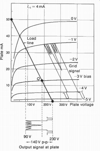
FIGURE 13-6 LOAD-LINE CALCULATIONS FOR VIDEO AMPLIFIER CIRCUIT IN FIG. 13-5.
PLATE-CHARACTERISTIC CURVES FOR 6AW8-A PENTODE SECTION.
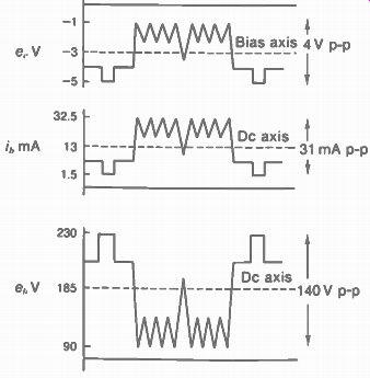
FIGURE 13- 7 VIDEO SIGNAL WAVESHAPES FOR LOAD LINE OPERATION IN FIG 13- 6
By means of the values on the load line, we can calculate the dc voltages. The Q point for 3-V bias sets the average plate current I at 13 mA. The I bRL voltage drop equals 5,000 x 0.013, or 65, V. Subtracting this 65-V drop from the Ebb supply of 250 V results in 185 V for the average dc plate voltage.
With 13-mA / _p and 4-mA screen-grid current, the total average cathode current equals 17 mA. Therefore, Rk has the value of 3/0.017, or approximately 180 ohm for the 3-V bias.
Similarly, R. is 25,000 if to produce a voltage drop of 100 V with 4-mA screen current.
This 100-V IR drop across Rs when subtracted from the supply of 250 V provides 150 V for the screen-grid voltage.
13-4 Manual Contrast Control
As the control is turned clockwise, more ac video signal is provided for the picture tube.
Greater variation between black and the whitest parts of the picture results, increasing the contrast.
Any control that varies the amount of ac video signal will operate as a contrast adjustment. Therefore, the contrast varies when the gain is varied in either the picture IF section or the video amplifier. The contrast control is in the video amplifier, however. The reason is that all receivers have automatic gain control to ad just the bias on the picture IF amplifiers automatically according to the signal level. Also, with intercarrier sound a variation of IF bias affects the sound volume.
The most common methods of contrast control in the video amplifier are shown in Fig. 13-8. In a the variable cathode resistor R1 varies the bias for the video amplifier. The control is unbypassed in order to provide degeneration of the ac signal. Then the amount of degeneration also varies as the bias resistor is varied. The degeneration is important for varying the gain because with linear amplification little change in gain results from changing the bias. Moving the variable arm of R, closer to the cathode end reduces the bias and the degeneration. This allows more gain to increase the video signal amplitude and the contrast. The variable emitter resistor R, for the transistor amplifier in b controls the contrast in essentially the same way.
The variable-bias method of contrast control has the disadvantage of changing the amplifier operating characteristics, which can introduce amplitude distortion. To overcome this problem, the arrangement in c taps off the desired amount of ac signal output without changing the bias. Now the contrast control R1 is a potentiometer in the video signal circuits.
As the variable arm of R2 is moved up to terminal 3 or maximum resistance, the video output increases for more contrast. This method is the same as a volume control for audio signal.
The stray capacitance of the potentiometer and its connecting leads can reduce the high-frequency response of the amplifier.
To minimize shunt capacitance, the control is usually mounted near the video amplifier with the shaft mechanically linked to the front panel of the receiver. In addition, the 27-pF C, is used as a compensating capacitor to keep the same frequency response at different settings of the contrast control.
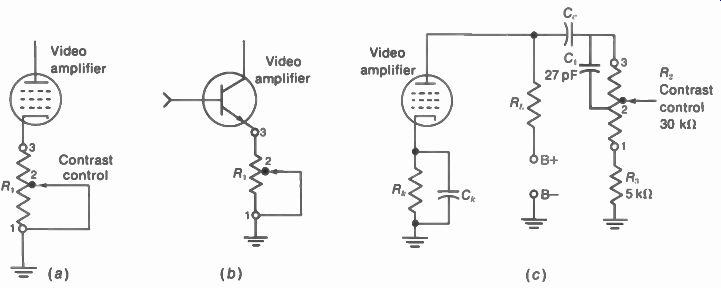
FIGURE 13-8 METHODS OF CONTRAST CONTROL IN VIDEO AMPLIFIER. (a) VARIABLE
CATHODE RESISTANCE. (b) VARIABLE EMITTER RESISTANCE. (c) VARIABLE POTENTIOMETER
TO TAP OFF AC SIGNAL VOLTAGE.
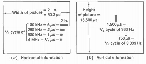
FIGURE 13-9 RELATION OF VIDEO SIGNAL FREQUENCIES TO SIZE OF PICTURE INFORMATION
SHOWN AS DARK BARS THESE ARE DRAWN TO SCALE WITH RESPECT TO FULL WIDTH AND
HEIGHT OF PICTURE. (a) IN HORIZONTAL DIRECTION (b) IN VERTICAL DIRECTION
(a) Horizontal information (b) Vertical information
13-5 Video Frequencies
The video stage amplifies signal voltage that may have frequency components from 30 Hz to 4 MHz. High frequencies are produced because the video signal contains, within a line, rapid changes in voltage that occur during very much less time than the active line-scanning time of 53.3 As. These fast variations in signal voltage can correspond to frequencies infinitely high, but are limited to approximately 4 MHz by the restriction of a 6-MHz transmission channel. Furthermore, receivers generally cut off the video frequency response at approximately 3.2 MHz in order to minimize interference with the chrominance signal at 3.58 MHz.
How to determine the period and frequency. See Fig. 13-9. Note that the visible picture width in a is translated into 53.3 As of time. This value is the total line time of 63.5 minus the horizontal blanking time of 10.2 u.s.
Similarly, the visible picture height in b is 1/60 s minus 7 percent vertical blanking.
To convert the size of an element of picture information into frequency, it is first necessary to calculate the time required to scan the element. This time can be considered as the period of a half-cycle of the video signal required to reproduce the information. Then you can
1. Multiply the time by 2 to obtain the period of a full cycle.
2. Take the reciprocal of the period. The answer is the desired frequency. With time in microseconds, the frequency is in megahertz.
Horizontal information. In Fig. 13-9a, the top black bar has a width slightly less than one-tenth of the picture width. Therefore, the bar is scanned horizontally in 5 /u.s. This time is a little less than one-tenth of 53.3 u.s for the entire picture width. As a result, the video signal for this black bar preceded and followed by white information corresponds to one-half cycle of a signal variation with a total period of 10 u.s for the full cycle. The corresponding frequency is = 0.1 MHz, or 100 kHz. Note that the width of this bar is 2 in. on a screen 21 in. wide.
The lowest frequency for picture information in the horizontal direction can be considered as 9.4 kHz, corresponding to a line all white or all black, producing video signal with a half period of 53.3 /25. The highest frequencies are produced by thin bars with the fastest variations in video signal.
Vertical information. The signal frequencies corresponding to picture information scanned in the vertical direction can be calculated in a similar manner (see Fig. 13-9b). Here the height of the black bars is converted to frequency in terms of active vertical scanning time equal to 0.0155 s. This is relatively low frequency information compared with details reproduced within a line. If the video voltage is taken from top to bottom, through all the horizontal lines in a field, this variation will correspond to a half-cycle of a signal with a frequency of approximately 30 Hz.
When the brightness of the picture varies from frame to frame, the resultant signal frequency is lower than 30 Hz. However, this is considered as a change in dc level, corresponding to a change in brightness of the scene.
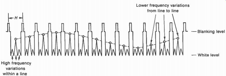
FIGURE 13-10 VIDEO SIGNAL WAVEFORMS. HIGH-FREQUENCY COMPONENTS ARE VARIATIONS
WITHIN EACH LINE OF HORIZONTAL SCANNING. LOWER-FREQUENCY VARIATIONS DURING
VERTICAL SCANNING ARE FROM LINE TO LINE WITHIN A FIELD.
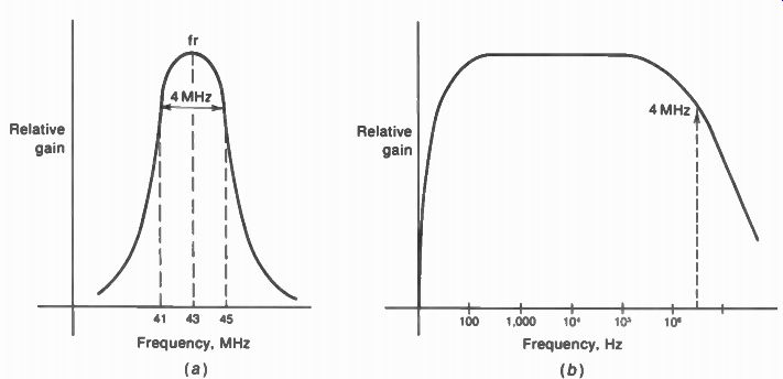
FIGURE 13-11 COMPARISON OF RESPONSE CURVES WITH 4-MHz BANDWIDTH. (a) TUNED
RESPONSE CENTERED AT 43 MHz. (b) WIDEBAND RESPONSE FROM LOW AUDIO FREQUEN
CIES UP TO 4 MHz.

TABLE 13-1 VIDEO AMPLIFIER SPECIFICATIONS
In summary, then, the ac video signal can be regarded as a complex waveform, not being a sine wave, containing signal voltages that range in frequency from 30 Hz to 4 MHz, approximately. Figure 13-10 illustrates typical video signal waveshapes. Note that the high-frequency variations correspond to white, gray, and black shadings across every line. The lower frequency variations correspond to vertical shadings of gray, black, and white.
Wideband amplifiers. The video amplifier is a good example of a wideband amplifier, which can be defined as a stage that amplifies both audio frequencies and radio frequencies. To see the difference in frequency response between a wideband amplifier and a tuned amplifier with wide bandwidth, refer to Fig. 13-11. In a, the response curve is for an IF amplifier tuned to 43 MHz. Its bandwidth is 4 MHz, meaning it can amplify the band of frequencies from 41 to 45 MHz with 70.7 percent response or more. however, the video amplifier frequency response in b is entirely different, although it also has a bandwidth of 4 MHz. Here the bandwidth includes audio frequencies from 30 Hz and radio frequencies up to 4 MHz. This response is really an example of amplifying a wide range of frequencies because the ratio of the highest to the lowest frequency is very great.
For wideband amplifiers it is convenient to consider the bandwidth in octaves. An octave is a range of 2 to 1 in frequency. As examples: from 100 to 200 Hz is 1 octave; 400 Hz is 1 octave above 200 Hz. Note that 100 to 400 Hz is a range of 2 octaves, as each octave means doubling the frequency.
The applications of wideband amplifiers include circuits that must amplify sine waves of audio and radio frequencies, or amplification of complex waveforms having a wide range of sine wave frequency components. Common examples are amplifiers for the input signal in an oscilloscope, pulse amplifiers, and video amplifier circuits. The bandwidth requirements for typical video amplifier applications are listed in Table 13-1.
13-6 Frequency Distortion
The amplifier has more gain for some frequencies than for others. Excessive frequency distortion cannot be tolerated because it changes the picture information. As shown in the amplifier response curve of Fig. 13-12, the amplifier response should be flat within a tolerance of about 10 percent. Note that the frequency units are marked off on the horizontal axis in powers of 10, making the spacing logarithmic. This spacing is necessary for a graph of reasonable size that will still show the ends of the response curve.
When the amplifier has a flat response curve, the relative gain of the amplifier is the same for all signal frequencies. Then the amplifier introduces no frequency distortion. As an example, the 100 percent response in Fig. 13-12 may correspond to a voltage gain of 35 at the middle frequency of 10 kHz. Then the flat response means the gain is 35 for all frequencies from 30 Hz to 4 MHz. With an actual video signal containing typical picture information coupled to the amplifier, the different frequency components do not all have the same amplitude. When the amplifier response is flat, however, all frequencies are amplified equally well without any frequency distortion. Then each frequency component in the amplified output signal has the same relative amplitude as in the input signal.
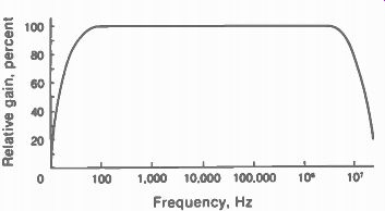
FIGURE 13-12 DESIRED FLAT FREQUENCY RESPONSE OF VIDEO AMPLIFIER.
Usually the response of the uncompensated video amplifier is down for the high video frequencies of 1 MHz and above. High frequency compensation is necessary, therefore, for a flat frequency response up to 3.2 MHz.
Video frequencies up to 4.2 MHz are broadcast by the transmitter, but the video amplifier in the receiver generally cuts off at 3.2 MHz, in order to minimize interference with the 3.58-MHz chroma signal.
At the low-frequency end, the video amplifier response can be down at about 100 Hz and below. Then low-frequency correction of the video amplifier may also be necessary. The response of the video amplifier over the middle range of frequencies is normally flat and requires no compensation.
Loss of high video frequencies. If these signal frequency variations are lost, the rapid changes between black and white for small adjacent picture elements in the horizontal lines cannot be reproduced, with the resultant loss of horizontal detail. Figure 13-13 shows the effect of loss of the high video frequencies on the reproduced test pattern. Notice the lack of separation between the black-and-white divisions in the top and bottom wedges. The extent to which the divisions in either of these wedges can be resolved indicates the high-frequency response.
The divisions all the way in to the center circle indicate video-frequency response up to 4 MHz.
The divisions in the widest part of the vertical wedges correspond to a video frequency of about 2 MHz.
FIGURE 13-13 TEST PATTERN ILLUSTRATING LOSS OF HIGH VIDEO FREQUENCIES. NOTE
LACK OF SEPARATION FOR THE LINES IN TOP AND BOTTOM WEDGES. ALSO. THEY HAVE
WEAKER INTENSITY THAN THE SIDE WEDGES. (RCA PICT-O-GUIDE)
FIGURE 13-14 TEST PATTERN ILLUSTRATING LOSS OF LOW VIDEO FREOUENCIES. BACKGROUND
IS WEAK, AND LETTERING IS NOT SOLID. SIDE WEDGES HAVE WEAKER INTENSITY THAN
TOP AND BOTTOM WEDGES. (RCA PICT-o-GUIDE)
In a televised scene, loss of the high video frequency information is evident as reduced de tail. The picture does not appear sharp and clear. Small details of picture information, such as individual hairs in a person's eyebrows and details of the eye, are not reproduced. In addition, the edges between light and dark areas, as in the outline of lettering or in the outline of a person's face, are not reproduced sharply but trail off gradually instead.
The effects of reduced high-frequency response causing insufficient detail in the picture are not so noticeable when the camera at the studio presents a closeup view. Then the subject occupies a large area of the picture, and the highest video signal frequencies are not so necessary.
Loss of low video frequencies. The video frequencies from about 100 kHz down to 30 Hz represent the main parts of the picture information, such as background shading, lettering, and any other large areas. This follows from the fact that it takes a longer period of time for the video signal to change over large areas. Frequencies from 100 down to about 10 kHz correspond to black-and-white information in the horizontal direction having a width one-tenth or more of a horizontal line. Frequencies from 10 kHz down to 30 Hz can represent changes of shading in the vertical direction. If a solid white frame is scanned, the signal is a 30-Hz square wave. If this low-frequency square wave is not amplified with its waveshape preserved, the reproduction will show a white screen having a gradual change of intensity from top to bottom.
Figure 13-14 shows a test pattern reproduced with insufficient low-frequency response.
The background is dull gray, instead of white, and the lettering is not solid. Actually, the picture as a whole is weak with poor contrast because low video frequencies represent the main areas of picture information. Notice that the side wedges, which represent low video frequencies, are weaker than the top and bottom wedges, which correspond to the high video signal frequencies. The changes from black to white in the vertical direction between the divisions in the side wedges represent frequencies of 4 to 8 kHz, approximately.
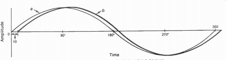
FIGURE 13-15 PHASE DELAY WAVE b LAGS BEHIND WAVE a BY THE AMOUNT OF TIME
EQUAL TO 10 OF THE CYCLE
13-7 Phase Distortion
The effect of phase distortion is time delay. The relative time delay of some parts of the video signal with respect to the others is important because one element of the picture is being reproduced at a time as the scanning beam traces out the frame. As a result, a great enough time-delay distortion in the video signal can have the effect of displacing the picture information on the picture tube screen. The result is smear in the picture.
Time delay. Phase delay is equivalent to time delay. If one signal voltage is 10 out of phase with another and lagging, as shown in Fig. 13-15, it reaches its maximum and minimum values at a later time. The delay is the amount of time that corresponds to 10: of the cycle. This time varies with the frequency. For a signal voltage having a frequency of 100 Hz, it takes t/„„, s for one complete cycle of 3600. The amount of time equivalent to 10' in the cycle is 1 "/: ,„„ x '/„„, s which is approximately 0.000278 s or 278 u.s.
In this time the scanning beam can be displaced in a vertical direction by more than four lines.
Phase distortion is very important at low video frequencies, therefore, because even a small phase delay is equivalent to a relatively large time delay. For the extremely high video frequencies, the effects of phase distortion are not as evident on the screen because the time delay at these high frequencies is relatively small. Normally, a video amplifier stage that has flat-frequency response up to the highest useful video frequency has negligible time-delay distortion for the high frequencies.
Square-wave response. Consider the wave shape shown at the right in Fig. 13-16a. This wave is actually composed of two sine waves.
One is the fundamental, with the same frequency as the combined waveform. The other sine wave is the third harmonic, having a frequency 3 times the fundamental frequency and an amplitude one-third of the fundamental.
Addition of the two sine waves, fundamental and third harmonic, produces the resultant non sinusoidal wave. This wave has the same frequency as the fundamental but tends to become more of a square wave than a sine wave.
If enough odd harmonics are added to the fundamental, the result will be a square wave.
The waveshape resulting from combining the fundamental and its harmonics is critically dependent on the phase relation between the waves. Figure 13-16b shows the combination of the same fundamental and third harmonic as in a, the amplitude and frequency of each being preserved, but with a different phase angle between the two waves. Assume that in a stage amplifying such a signal the fundamental and third harmonic are originally in phase, as shown in a. Then because of phase distortion, the fundamental is made to lag by 600 of its cycle, and the third harmonic is made to lag by 1200 of its cycle, with the result shown in b. The resultant waveshape is distorted from the original wave because the original phase relations between the fundamental and harmonic are not maintained.
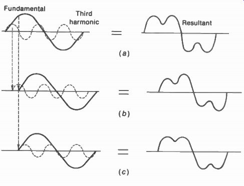
FIGURE 13-16 HOW PHASE DISTORTION CHANGES WAVESHAPE OF NONSINUSOIDAL SIGNAL
(a) FUN DAMENTAL AND THIRD HARMONIC IN PHASE. (b) FUNDAMENTAL DELAYED BY 60
AND THIRD HARMONIC BY 120. PHASE DELAY NOT PROPORTIONAL TO FREQUENCY. (c)
FUNDAMENTAL DELAYED BY 60 deg. AND THIRD HARMONIC BY 180 deg. PROPORTIONAL
TO FREQUENCY.
Phase distortion always produces an unsymmetrical distortion of the waveshape, as in b.
Notice that the peak amplitudes of the wave in b have different values than the original wave, and they occur at different times than the peaks for the undistorted wave. When the signal amplitudes are distorted this way, the corresponding picture information has incorrect light values and is displaced in time, producing smear in the reproduced image (see Fig. 13-17). Phase shift should be proportional to frequency. It is important to note that the phase distortion is introduced because the amount of phase shift is not proportional to frequency.
The distortion is not caused by the phase shift in itself. When the second harmonic is delayed twice as much as the fundamental, the third harmonic 3 times as much, and so on, then the phase shift is proportional to frequency and there is no phase distortion. As an example, in Fig. 13-16c the third harmonic is delayed by 180 deg which is 3 times 60 deg. Then the phase shift of the fundamental and third harmonic is proportional to frequency. As a result, there is no phase distortion, and the wave maintains its original shape.
FIGURE 13-17 SEVERE SMEAR CAUSED BY EXCESSIVE LOW-FREQUENCY RESPONSE WITH
PHASE DISTORTION. (RCA PICT-O-GUIDE)
To see why the phase shift should be proportional to frequency, the phase delay must be translated into time delay. Consider a 1,000-Hz signal, corresponding to the fundamental frequency in Fig. 13-16, delayed by 60°. This is a delay of 6136t of the complete cycle that takes _s. The amount of time delay can be calculated from the formula ti 1 T, = x - 360 1
In this example, 60 1 1 360 1,000 6,000 (13-1)
When a 3,000-Hz signal corresponding to the third harmonic of the fundamental is delayed by 180 degr, the amount of time delay is 180 1 1 360 3,000 6,000
This is the same amount of time delay as for the fundamental. With phase shift proportional to frequency, therefore, the time delay is uniform.
The time delay is not harmful if all frequency components have the same amount of delay. The only effect of such uniform time delay would be to shift the entire signal to a later time. No distortion results because all components would be in their proper place in the video signal waveshape and in the picture. Therefore, the phase angle should be proportional to frequency, as illustrated by the linear graph in Fig. 13-18a, which provides the uniform time delay in b.
It should be noted that signal inversion of exactly 180° in the video amplifier does not mean phase distortion. This is no time delay, only a polarity reversal.
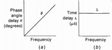
FIGURE 13-18 PHASE RESPONSE (a) PHASE ANGLES PROPORTIONAL TO FREQUENCY (b)
CORRESPONDING TIME DELAY THAT IS CONSTANT
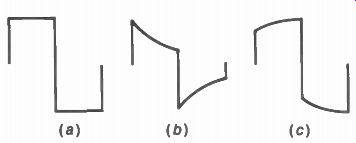
FIGURE 13-19 SQUARE-WAVE TESTING. (a) INPUT FROM SQUARE-WAVE GENERATOR. (b)
LOW-FREQUENCY DROOP. (c) LOW-FREQUENCY RISE.
In practical terms, low-frequency distortion in the video amplifier can be caused by leak age in the coupling and bypass capacitors. The reduced capacitance results in reactance too high for low-frequency signals.
Square-wave testing. The best check for phase distortion is to test the amplifier with input from a square-wave generator at the desired frequency. This waveform is critically dependent on the phase-angle response of the amplifier. Figure 13-19 shows the input square wave in a and distorted output in b or c. The typical low-frequency droop in b indicates too little capacitance in a coupling circuit. The nonlinear top and bottom on this waveform are actually parts of the capacitor charge and discharge curves, as the RC time constant is not long enough. The opposite effect is shown by the rise at the top and bottom of the waveform in c. This distortion can be caused by excessive gain for low frequencies, usually with reduced response for high frequencies.
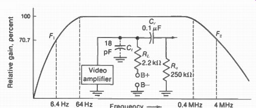
FIGURE 13-20 FREQUENCY RESPONSE WITH SPECIFIC VALUES FOR RC-COUPLED AMPLIFIER.
13-8 High-Frequency Response of the Video Amplifier
As shown in Fig. 13-20, the resistance load R1 , makes the response flat over a wide range of middle frequencies. Therefore, an RC-coupled stage is best for amplifying the wide band of video frequencies with minimum frequency and phase distortion. Audio-transformer coupling would not be suitable for the high video frequencies that correspond to radio frequencies. A video frequency of only 2 MHz is higher than any rf signal in the standard radio broadcast band.
This entire band from 535 to 1,605 kHz would occupy only a small part of the video spectrum from 30 Hz to 4 MHz. Coupling with rf trans formers would not be suitable for the lowest video frequencies that correspond to audio frequencies.
The examples shown in Figs. 13-20 to 13-24 apply to video amplifiers using either tubes or transistors. However, wideband response for high frequencies is less of a problem with transistor amplifiers because of their relatively low input and output resistances.
Total shunt capacitance. The video amplifier gain is down at the high-frequency end because of the shunting effect of capacitances to chassis ground, in parallel with R_L. All these capacitances add in parallel to provide the total value labeled Ct in Fig. 13-20. Typical values for Ct are 15 to 30 pF. This may seem small, but remember that capacitive reactance is inversely proportional to frequency. For the high video frequencies the capacitive reactance of Ct is low enough to reduce the load impedance Z_L. This consists of R_L in parallel with the reactance of Ct. The gain of the amplifier is down in the same proportion as the decrease in Z_L.
Miller effect. This is a dynamic increase of input capacitance in an amplifier. The cause is capacitive feedback of output signal to the input circuit. This is the reason why triodes are seldom used for video amplifiers, as they have a large grid-plate capacitance, compared with pentodes. The Miller effect increases with more gain. As an example, for a triode amplifier with 3 pF for C_gp and a gain of 20, the capacitance added to the input circuit is approximately 20 x 3 = 60 pF.
Load resistor. Video stages use a low value of Rt, compared with audio amplifiers. Typical values are 2,000 to 8,000 ohm. Although the gain is reduced, lowering R_L extends the high frequency response.
The effect of Ct does not become important until its reactance is low enough to becom parable with the resistance of R_L. Then the shunt reactance X_Ct lowers the impedance Zt. As examples, suppose R_L is 2,000 ohm and X_Ct, is 1 M-ohm. Then Z_L for the two in parallel is practically 2,000 ohm, the same as R_L. The reason is that a parallel path has little effect when it has very high ohms and very little current. However, if Flt were also 1 MIL the combined impedance would then be reduced to 70.7 percent of either one, for equal resistance and reactance in parallel.
High-frequency cutoff F_2. Specifically the gain is down to 70.7 percent of maximum response for the frequency where X-Ct= RL. This frequency, called the cutoff frequency F_2, can be calculated from this formula:
F2 =1 / 2 pi R_L Ct (13-2)
R_L is in ohms and Ct in farads to find F_2 in Hz.
For the example in Fig. 13-20 with R_L, of 2.2 k-O and Ct of 18 pF.
F2 -= 4 x 10^6 = 4 MHz
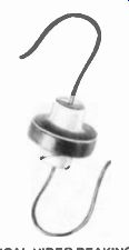
FIGURE 13-21 TYPICAL VIDEO PEAKING COIL. WIDTH IS 0.5 IN. L IS 180 µH.
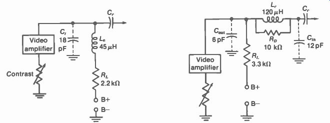
FIGURE 13-22 VIDEO AMPLIFIER WITH SHUNT PEAKING COIL L_D.

FIGURE 13-23 VIDEO AMPLIFIER WITH SERIES PEAKING COIL L_c.
FIGURE 13-24 VIDEO AMPLIFIER WITH SERIES-SHUNT COMBINATION PEAKING FOR HIGH-FREQUENCY
COMPENSATION AND R,C, DECOUPLING FILTER TO BOOST LOW FREQUENCY RESPONSE
TABLE 13-2 COMPARISON OF HIGH-FREQUENCY PEAKING METHODS
Ftt has the relatively low value of 2,200 ohm here for the F 2 of 4 MHz, where the gain is down 30 percent. Note that the response curve in Fig. 13-20 shows the gain is flat to the frequency
0.1 F 2 = 0.4 MHz = 400 kHz.
The lower Rt is and the smaller the shunt capacitance C _p the better is the high-frequency response. However, practical video amplifiers generally use higher values of Rt with peaking coils to boost the gain for high frequencies. A typical peaking coil is shown in Fig. 13-21.
Shunt peaking. See Fig. 13-22. This circuit is shunt peaking because L„ in the branch with R, is in parallel with C,. L„ can be connected on either side of Rt. The peaking coil resonates with C, to boost the gain for high frequencies, where the response of the uncompensated RC-coupled amplifier would drop off. With shunt peaking, the response is practically flat up to F, instead of 70.7 percent gain at this frequency. Because it is a small coil with little resistance, the peaking coil does not affect the dc voltages and the response at the middle frequencies. A peaking coil is effective for frequencies above 400 kHz, approximately.
Series peaking. See Fig. 13-23. In this circuit Lc is in series with the two main components of Ct. At one side of Lc. is C_out for the video amplifier, and on the other side is C_in of the next stage.
The series peaking circuit has more gain than shunt peaking because there is less shunt capacitance across RL, while Lc, provides a resonant rise of voltage across C_in. A series peaking coil usually has a shunt damping resistor, such as the 10-k-O, R_D. Its function is to prevent oscillations or ringing in the coil with abrupt changes in signal. For the same frequency response, series peaking can use R_L 50 percent higher with 50 percent more gain, compared with shunt peaking.
Combination peaking. The circuit in Fig. 13-24 combines shunt and series peaking. Of the three methods, combination peaking has the most gain. For the same frequency response can be 80 percent higher with 80 percent more gain, compared with shunt peaking. Values for these three peaking circuits are compared in Table 13-2.
Sharpness control. The circuit in Fig. 13-24 is shown with a variable resistor R1 that adjusts the high-frequency response of the video amplifier. This is similar to a tone control in an audio amplifier to vary the amount of bypassing at the high-frequency end of the response. R1 is generally called a sharpness, fidelity, or peaking control. Its purpose is to reduce the effect of interfering noise at high video frequencies, if necessary. The interference can be noise pulses, with weak signal, or beat frequencies between the luminance signal and 3.58-MHz chrominance signal. In Fig. 13-24, less resistance for R, results in more bypassing through the 39-pF C1. The result is reduced high-frequency response. With R, at maximum, there is no by passing for maximum sharpness in the picture. A choke can also be used, instead of the capacitor, in series with the variable resistor as the sharpness control.
13-9 Low-Frequency Response of the Video Amplifier
Remember that for lower frequencies the capacitive reactance increases. This is a problem for coupling and bypass capacitors, which should have very low reactance.
Low-frequency cutoff F. With an RgCc coupling circuit, specifically, the signal voltage across Rg for the next stage is reduced to 70.7 percent of maximum at the frequency when
…
This frequency can be calculated from the formula
F1 = 1/ 2 pi – RgCc (13-3)
R, is in M-O and C. in ; IF to find F, in Hz.
For the example in Fig. 13-20 with 0.1 uF for C,. and
0.25 M-O for Rg, F, - 2 pi R„C,. 2.7 x 0.25 x 0.1 1 1
0.16 / 0.025
F1 = 6.4 Hz
In this example, then, the low-frequency gain is down 30 percent at 6.4 Hz because of the reactance of C. Note that the response curve in Fig. 13-20 shows the gain is flat to 10 x F1 = 64 Hz.
Low-frequency compensation. The low-frequency response can be improved by using the largest possible values for the bypass capacitors and RC coupling circuit. In addition, the decoupling filter Rf Cf in the B+ supply line in Fig. 13-24 can be used to boost the gain and reduce phase distortion for very low frequencies. This low-frequency compensation can be used in any RC-coupled amplifier. Note the 0.005-µF C2 in parallel with the 10-µF Cf. C2 is a small paper or ceramic capacitor for the high video frequencies not bypassed because of the small inductance of Cf , which is a tubular electrolytic capacitor.
For the very low frequencies, C f has enough reactance to provide appreciable impedance Z f for the RfC, combination. Then Z, in series with R1 , boosts the gain for low frequencies. The reason for the increased gain is a higher 4. The rise in gain compensates for the reduced signal output caused by the increasing reactance of C,.. Furthermore, the phase shift caused by the shunt C f is opposite from the phase angle of the series C,.. As a result, C, corrects phase distortion introduced by the coupling circuit. Typical values for C , are 2t0 10 µF. R, should be 10 times larger than X ( . 1 , or more, at the lowest frequency. However, too high a value for R f drops the supply voltage too much. The time constant of R,Cb . = R„C,. for low frequency compensation.
FIGURE 13-25
13- 10 Video Amplifier Circuits
Input signal of 1 to 3 V is supplied by the video detector. This composite video signal must be amplified for about 100-V output, peak to peak. The signal from the video detector usually has negative sync polarity, which is inverted by the video amplifier to positive sync polarity for the cathode of the picture tube. The circuits in Figs. 13-25 and 13-26 illustrate video amplifiers in monochrome receivers. The idea of how the video section serves as the amplifier for luminance signal in color receivers is illustrated in Fig. 13-31.
Single-tube video amplifier. In Fig. 13-25, the video detector diode X1 is dc-coupled to the video amplifier stage. Then the required negative grid bias of 2 V is supplied by the dc component of the detected video signal. In the plate circuit, the 5.6-k-O R7 is the load resistor. The shunt peaking coil is L8 with L9 used for series peaking. Note that L9 is wound on a 4.7-k-O resistor for damping. The amplified video output is coupled to the cathode of the picture tube by the 0.1-µF C23 . Since the control grid returns to ground through the 15-k-O R4, the video signal is applied to the cathode-grid circuit. With peak to-peak signal output of 125 V for input of 2.6 V, the voltage gain of the video amplifier stage is 125/2.6 = 48.
Note that the 4.5-MHz intercarrier sound signal is taken from the plate circuit of the video amplifier. The primary winding of T6 tunes with C18 as a 4.5-MHz trap to keep the sound out of the picture. However, the secondary winding L7 has the 4.5-MHz sound signal coupled by C21 to the grid of the first sound IF amplifier. The dc R of each coil is marked on the diagram.
The contrast control is the 30-k-O. R8 in the plate circuit of the video amplifier. It varies the amount of video signal coupled by C23 to the picture tube. The small capacitors C21, C22, and C24 compensate for the capacitance of the contrast control as its resistance is varied. The peaking control is the 1,500-ohm. R5 in series with L4 in the video detector output circuit. The brightness control is the 250-k-O. R9. It varies the dc voltage at the cathode of the picture tube, from the 280-V supply.
The video amplifier has outputs for sever al circuits in addition to the picture tube. High frequency peaking is not necessary for these connections because only the signal amplitudes are important. The voltage divider consisting of R1, R2, and R3 in the plate circuit supplies video signal for the AGC stage and sync clipper. DC coupling is used for the AGC circuit, which rectifies the video signal to provide AGC bias proportional to signal strength. The sync clipper separates the sync for the deflection circuits.
An additional output in Fig. 13-25 is video signal from the detector to a noise gate. This circuit eliminates the effect of noise pulses in the sync and AGC circuits. Video signal from the detector is used for the noise gate because this polarity is opposite from the output of the video amplifier.
For the picture tube in Fig. 13-25, note that vertical blanking pulses are coupled to the screen grid. These are negative pulses, taken from the vertical deflection circuit, to cut off beam current during vertical retrace time. Most receivers have this internal vertical retrace suppressor circuit. The vertical blanking pulses can also be coupled to the control grid, or cathode of the picture tube, or into the video amplifier to become part of the video signal. In addition, the receiver may use blanking pulses from the horizontal deflection circuit to eliminate horizontal retraces.
Emitter-follower driving CE amplifier. In Fig. 13-26, signal from the video detector is dc coupled to the base of Q1. This is an NPN transistor that combines the functions of an emitter follower and CE amplifier. The emitter load resistor R2 of 470 it results in a high input impedance at the base, to minimize loading of the video detector. Remember that the emitter output signal has the same polarity as the base input signal. The collector load resistor is the R, of 1.8 k-Ohm. There are two output signals, isolated by the separate output circuits. The video signal from the collector goes to the sync clipper. The video signal from the emitter goes to the base of Q2. This is a 5-W power transistor, with a heat sink mounted on the case. The collector supply is 140 V, to provide enough voltage swing for the 80-V peak-to-peak video signal output. In addition to driving Q2, the emitter output of Q1 supplies video signal for the AGC stage and for the 4.5-MHz intercarrier sound signal.
In the output circuit of Q2, the contrast control R4 and R„ in series provide a total collector load resistance of 6.8 ki2. The video output signal is coupled by the 0.22-µF C, to the cathode of the 12-in, picture tube. L2 is a series peaking coil. The control grid returns to ground for the video signal through the 15-k-ohm R,0. The neon bulb in the grid circuit provides the protection of a spark gap, as the bulb ionizes and shorts to ground with excessive voltage. For brightness control, the 100-k-ohm R, varies the dc voltage at the cathode, from the 140-V supply in series with the 56-k-ohm. R8.
Note the dc voltages for the two transistors. Q1 has forward bias of 2.4 - 1.8 = 0.6 V. TFe 2.4 V at the base is the dc output of the video detector. The 1.8 V at the emitter is the IR drop across R, produced by emitter current. This 1.8 V at the emitter of Q1 is the base voltage at Q2 because of the direct coupling. For D2 its forward bias is 1.8 - 1.2 = 0.6 V. The value of 0.6 V is typical forward bias for a silicon transistor amplifier operating class A.
FIGURE 13-26 TRANSISTORIZED VIDEO CIRCUIT WITH EMITTER-FOLLOWER DRIVING CE
AMPLIFIER FOR VIDEO OUTPUT STAGE (FROM RCA HSK TI CHASSIS)
FIGURE 13-27 VIDEO DETECTOR. (a) DIODE CONNECTED FOR NEGATIVE OUTPUT ACROSS
R, IN ANODE CIRCUIT. (b) TYPICAL DETECTOR DIODE. LENGTH IS 7, IN. BAND AT
CATHODE END. (GE)
13-11 The Video Detector Stage
As shown in Fig. 13-27, the input to this diode detector is the modulated IF picture carrier signal, which is rectified and filtered. Rectification allows the amplitude variations to be extracted, while the filtering removes the carrier. As a result, the detected output corresponds to the modulation envelope of the IF signal. This envelope is the original composite video signal with all the information needed for the picture, including sync and blanking. A diode needs about 3-V IF signal for linear detection, without distortion.
The video detector is a signal diode, usually silicon or germanium, in a glass package V, in. long. A stripe at one end marks the cathode side. One type is the 1N3064, rated at 60V for reverse breakdown and 10 mA maximum forward current. The detector is often in side the shield can of the last IF transformer, as indicated for the diode X1 in Fig. 13-25. Shielding is generally used for the detector stage in order to prevent harmonics of the detected signal from radiating back to the rf and IF stages. With an integrated circuit for the IF amplifier, the video detector is usually part of this IC unit.
Diode detection. The video detector action is the same as any diode detector for an AM signal.
In Fig. 13-27, the signal input provides ac voltage to drive the diode into conduction as a half wave rectifier. No dc supply voltage is used for the detector because the signal makes the diode conduct. The signal can be applied either to the anode or to the cathode. At the anode, the positive half-cycles of input signal produce forward current in the diode. At the cathode, the negative half-cycles of IF signal are detected. Negative polarity is shown in Fig. 13-27 because the video detector is often connected this way.
Electron flow for i is from the top of L s, from cathode to anode in D1, through R1 _p and returning to the grounded side of L. With more ac input, the diode current increases. The tip of sync in the signal produces maximum current. Less input for white signal amplitudes reduces the current. As a result, the current i consists of half-cycles of the IF carrier signal with varying amplitudes. These variations correspond to the envelope of the AM carrier signal.
Since the voltage across R1 , is iRL, the output 14,1, has the same signal variations as the current. The capacitance C, across R1 , filters out variations at the IF rate so that the output voltage includes only the lower-frequency variations of the envelope. This is the composite video signal output voltage of the detector. In this example, the variations between tip of sync and white in the signal provide output of 3 V, peak-to-peak.
The detector load resistance R1 , has shunt capacitance C _p with the peaking coils L „ and L ,. that provide the same response for high video frequencies as required in the video amplifier.
Similarly, the relatively low value of 2 to 8 k ohm is used for R1 , for good high-frequency response.
The video detector is the input circuit for the video amplifier section.
It is necessary to rectify the modulated carrier signal because its amplitude variations have an average value of zero, as a result of the symmetrical envelope. In terms of the desired video signal information, the carrier is just as much positive as negative at any one instant of time. However, after rectification the amplitude variations of the modulation can be obtained as variations in the amount of rectified carrier signal. The detector output voltage across R _p, therefore, is the desired video signal.
Detector polarity. Both sides of the modulation envelope have the same amplitude variations. Therefore, either polarity of the IF signal can be rectified by the detector. Depending on whether R, is in the anode or cathode circuit, a diode can produce either negative or positive dc output voltage. In Fig. 13-27, R1 , is in the anode return to ground. Then the detected signal is a varying dc voltage of negative polarity. The sync produces the most output, resulting in negative sync polarity for the composite video voltage.
Also, the average level of the detector output is a negative dc voltage. In this example, the dc output voltage of the detector is -2 V. If the diode were reversed in Fig. 13-27, the detector output would be positive. Then the IF signal would be applied to the anode, with R _p in the cathode circuit. The average level of the detector output would still be 2 V, but positive.
Also, the video signal would have positive sync polarity.
It may be of interest to note that detector polarity does not matter in a sound system. The reason is that the loudspeaker is driven by ac audio signal, without any dc bias. For the picture tube, though, polarity inversion of the video signal produces a negative picture.
Dc level of the detector output. An important feature of the detector output is that it consists of a varying dc voltage. The detector diode is just a low-power rectifier, or signal diode, to change the ac input to dc output.
More details of the detector output voltage are shown in Fig. 13-28. In a, the dc axis of -2 V is the average level. A dc voltmeter can be used to read this dc level of -2 V. Peak-to-peak ac signal. The video signal is in the variations of the dc voltage. In Fig. 13-28a the peak voltage is-4 V and the minimum is -1 V. Therefore, the peak-to-peak amplitude for the signal voltage variations is 3 V. No polarity is assigned to the ac component.
In Fig. 13-28b, the ac signal is shown without the dc level, which is blocked by a coupling capacitor. The dc axis in a becomes the average level of zero in b for the ac signal. In both cases, the peak-to-peak amplitude is 3 V for the variations in signal voltage. The 3-V signal is typical for driving a video amplifier tube.
For transistors, the signal output of the video detector is about 1 V, peak-to-peak.
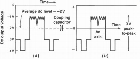
FIGURE 13-28 VIDEO DETECTOR OUTPUT VOLTAGE. (a) DC FORM (b) AC FORM AFTER
AVERAGE DC COMPONENT IS BLOCKED BY COUPLING CAPACITOR.
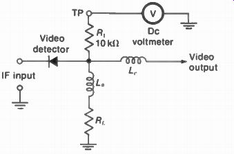
FIGURE 13-29 MEASURING RECTIFIED IF SIGNAL WITH DC VOLTMETER AT VIDEO DETECTOR
TEST POINT.
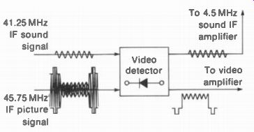
FIGURE 13-30 THE VIDEO DETECTOR CAN PRODUCE THE 4.5-MHz INTERCARRIER SOUND
SIGNAL. IN ADDITION TO THE COMPOSITE VIDEO SIGNAL.
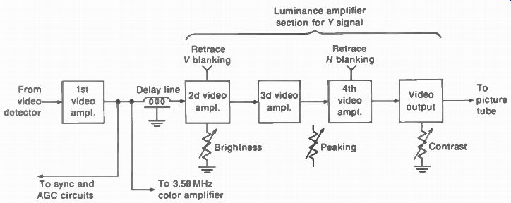
FIGURE 13-31 LUMINANCE SECTION TO AMPLIFY Y VIDEO SIGNAL IN THIS IS A TRANSISTORIZED
CIRCUIT. (FROM RCA CTC 40 CHASSIS) COLOR RECEIVER
Video detector test point. Most receivers have a test point (TP) to measure the video detector output from the top of the chassis. As shown in Fig. 13-29, R, of about 10 M-o is used to isolate TP. A dc voltmeter here is a convenient measurement because a dc meter is used to check IF signal. The dc level of the rectified signal is typically 2 or 3 V for vacuum tube amplifiers.
With transistors, this dc voltage is about 0.5 V. When the receiver is switched off channel to remove the signal input, the detector output drops to a lower value. The small output voltage without signal is rectified receiver noise.
When the detector dc output voltage has its normal value on channel and drops close to zero off channel, these checks mean the IF amplifier is operating with normal signal. If the output is close to zero, both off channel and on channel, there is no detected IF signal. If the detector output is very high on channel or off channel, this means the IF amplifier is oscillating.
An oscilloscope at the detector test point will show the composite video signal output. A typical value is 3-V peak-to-peak ac signal for a video amplifier tube. For a transistor video amplifier, the detector output is approximately 1 V. peak-to-peak. When the oscilloscope internal sweep frequency is at 30 Hz, you see two fields of video signal with the vertical blanking and sync pulses. When the sweep is at 7,875 Hz, you see two lines of video signal with the horizontal blanking and sync pulses. For a color broad cast, you see the colorplexed composite video signal, with 3.58-MHz color burst on the back porch of horizontal sync and 3.58-MHz chrominance signal in the video. It should be noted, though, that individual cycles at 3.58 MHz are not visible unless you raise this sweep frequency and expand the sweep to magnify the pattern.
Detecting the 4.5-MHz intercarrier beat. In addition to the fact that the video detector diode rectifies the modulated IF picture carrier to re- cover the composite video signal, this stage serves as a frequency converter to produce the 4.5-MHz second sound IF signal (see Fig. 13-30). In terms of intercarrier sound, the 45.75-MHz picture carrier in the detector stage is equivalent to a local oscillator. The heterodyning action of the 45.75-MHz picture carrier beating with the 41.25-MHz center frequency of the sound signal results in the lower center frequency of 4.5 MHz.
This FM signal can then be coupled to the 4.5-MHz sound IF section for amplification and detection to recover the audio modulation.
In monochrome receivers, the video detector is used to supply the 4.5-MHz intercarrier sound signal. In color receivers, though, a separate diode is generally used as the 4.5-MHz sound converter. The reason is to reduce interference of the sound signal in the color picture.
13-12 Luminance Video Amplifier in Color Receivers
This section amplifies the Y signal without the 3.58-MHz chroma signal. Therefore, its function is the same as the video amplifier in a mono chrome receiver. The video bandwidth is cut off at 3.2 MHz in both cases to eliminate crosstalk from the 3.58-MHz color signal.
Figure 13-31 shows a block diagram of the video section for Y signal, from a solid-state color receiver. There are five video stages here, all dc-coupled from the detector to the picture tube. To provide a high impedance for the detector output, the first video stage is an emitter follower. This stage is often called a video preamplifier. It supplies output to both the 3.58-MHz color amplifier and the Y video amplifier. The second stage is a common base circuit to provide a low-impedance input to the delay line. A delay of approximately 1u-s is always used in the Y video amplifier so that the luminance and color signals will arrive at the picture tube at the same time. The circuits for luminance video signal have less delay because they are resistive, compared with the tuned circuits for the 3.58-MHz chroma signal. Note that the color signal is taken off before the delay line. In addition, video signal for the sync and AGC circuits is taken from the first video amplifier.
The third stage in Fig. 13-31 is a common emitter amplifier for the Y video signal. The fourth stage is an emitter-follower again, feeding the video output stage. This last stage is a power amplifier that supplies 120-V peak-to peak video signal to drive the three cathodes of the color picture tube. The signal has positive sync polarity here, resulting from positive polarity out of the video detector and two polarity inversions by the common-emitter amplifiers.
The contrast control is in the emitter circuit of the video output circuit to vary the gain for Y video signal. The peaking control in this circuit varies the amount of feedback for high video frequencies from the fourth stage back to the second stage. The brightness control varies the dc bias on the second video amplifier.
Because of the dc coupling, any change in dc level in the video circuits is coupled to the cathode of the picture tube. Similarly, instead of coupling the retrace blanking pulses to the picture tube, they are fed into the video amplifier.
This way the pulses are amplified while being coupled to the picture tube through the video section.
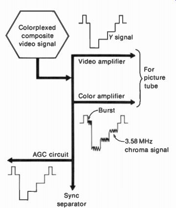
FIGURE 13-32 FUNCTIONS OF THE COMPOSITE VIDEO SIGNAL
13-13 Functions of the Composite Video Signal
Figure 13-32 illustrates four paths for the colorplexed signal obtained from the video detector.
We can consider that the signal is coupled to these parallel branches for the different functions. Therefore, each circuit can operate independently of the others. For instance, clip ping the synchronizing pulses in the sync separator stage does not interfere with the video amplifiers supplying signal for the picture tube.
Similarly, the AGC circuit rectifies the video signal for AGC bias, but the video amplifier provides the complete composite video signal. In color receivers, the luminance section amplifies the Y video signal without the 3.58-MHz chroma signal, while the 3.58-MHz bandpass amplifier supplies chroma signal for the color demodulators.
In summary, the four functions of the colorplexed composite video signal are as follows:
1. Video signal for the picture tube to put the picture on the raster
2. Supply vertical and horizontal synchronizing pulses for the sync circuits that time the deflection oscillators
3. Supply signal for the AGC circuit that controls the gain of the rf and IF stages to prevent overload distortion on strong signals
4. Supply 3.58-MHz chroma signal for the color amplifier to put color in the picture A comparison of the video circuits for monochrome and color receivers is shown in Fig. 13-33. Note the following additions for color receivers:
1. Separate diode converter stage for 4.5 MHz intercarrier sound.
2. Video preamplifier for sync and AGC takeoff circuits.
3. Delay line for Y video signal.
4. Y video amplifier to drive all three guns of the color picture tube with luminance signal.
5. Brightness control varies dc bias on Y video amplifier, dc-coupled to the color CRT. This method is used so that one control determines the bias on all three guns of the picture tube.
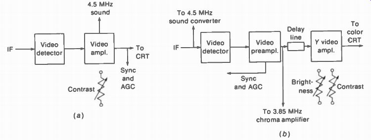
FIGURE 13-33 COMPARISON OF VIDEO CIRCUITS (a) MONOCHROME RECEIVER (b)
COLOR RECEIVER
13-14 The 4.5- MHz Sound Trap
The video amplifier usually has a trap tuned to the intercarrier sound frequency of 4.5 MHz to keep the sound signal out of the picture. In monochrome receivers, the 4.5-MHz trap is also the takeoff circuit for signal to the 4.5-MHz sound IF amplifier. The 4.5-MHz trap may be in the video detector or in the video amplifier.
Generally, the trap is in the video output in order to provide more 4.5-MHz signal for the sound section. This arrangement is shown in the video amplifier circuit in Fig. 13-25.
In color receivers, the luminance amplifier still has a 4.5-MHz trap to reduce 4.5-MHz beat in the picture. However, the 4.5-MHz trap is not used here for the sound takeoff. Color receivers generally have a separate sound converter stage to provide the 4.5-MHz intercarrier sound signal.
The reason is to reduce interference between the 4.5-MHz sound signal and 3.58-MHz chroma signal, which together produce a 920-kHz beat.
The 4.5-MHz sound signal in the picture produces about 225 pairs of thin, diagonal lines, with small wiggles like a fine herringbone weave. This effect in Fig. 13-34 is also called a "wormy" picture. The fine lines are produced by the 4.5-MHz carrier while the weave is the result of frequency variations in the FM sound signal.
When you observe the pattern closely, the her ringbone effect disappears when there is no voice or music, leaving just the straight lines corresponding to the 4.5-MHz carrier without modulation. If necessary, the 4.5-MHz trap can be tuned for minimum interference in the picture. The trap is just an LC circuit tuned to 4.5 MHz, as shown in Fig. 13-35.
Two trap circuits are illustrated in Fig. 13-36. In a, L, and C, form a parallel resonant circuit tuned to 4.5 MHz. The trap is in series with the output. Furthermore, the trap has maximum impedance at parallel resonance. Therefore, the trap frequency is removed because maximum voltage is developed across the trap itself. Note that L, in the trap is coupled to L 2 to provide the 4.5-MHz sound signal for the 4.5-MHz sound IF amplifier.
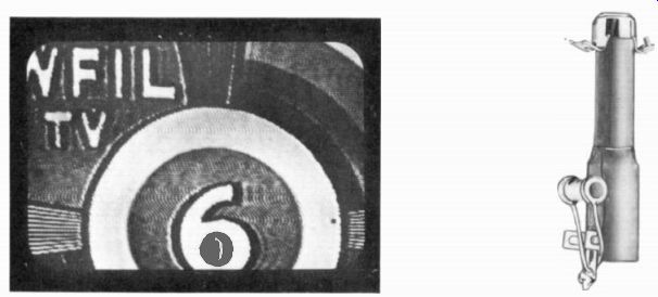
FIGURE 13-34 FINE HERRINGBONE WEAVE PRODUCED BY 4.5-MHz INTERCARRIER SOUND
IN PICTURE.

FIGURE 13-35 TYPICAL 4.5-MHz TRAP WITH L AND C. HEIGHT IS 17, IN.
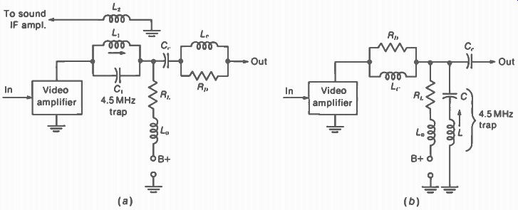
FIGURE 13-36 VIDEO AMPLIFIER CIRCUITS WITH 4.5-MHz TRAP. (a) PARALLEL RESONANT
TRAP IN SERIES WITH OUTPUT. TRAP HERE IS ALSO USED FOR SOUND TAKEOFF. (b)
SERIES RESONANT TRAP IN SHUNT WITH LOAD.
In Fig. 13-36b, Land C form a series resonant circuit tuned to 4.5 MHz. This trap circuit is in shunt with the load. Furthermore, the trap is practically a short circuit at series resonance.
As a result, the 4.5-MHz intercarrier sound is removed from the video output signal.
The trap has a coil with a variable slug.
Adjust for minimum 4.5-MHz beat in the picture.
SUMMARY
1. Composite video signal is coupled to the cathode-grid circuit of the picture tube to vary the beam current and screen illumination. This intensity modulation reproduces the picture information. Maximum beam current produces white; cutoff corresponds to black. About 100-V peak-to-peak video signal is needed for good contrast. Average brightness is set by the dc bias.
2. The video stage is a class A amplifier for minimum amplitude distortion, with RC coupling for wide frequency response. Peaking coils are used to boost the gain for high video frequencies.
3. The two most common methods of manual contrast control are: (a) variable resistor either in the cathode or in the emitter circuit to vary the gain; (b) variable potentiometer to tap off the desired amount of signal voltage. See Fig. 13-8.
4. In the range from 30 Hz to 3.2 MHz, higher video frequencies correspond to smaller details of picture information.
5. In an RC-coupled amplifier, the gain is down for high frequencies because the shunt capacitance C, has decreasing reactance that bypasses the load R1 ,. The frequency at which the gain is down to 70 percent response is F 2= 1 /(2 pi RLCi ).
6. The response is down for low frequencies mainly because the increasing reactance of the coupling capacitor C. results in less signal across R for the next stage. The frequency at which the gain is down to 70 percent response at the low end is F1=1/(2 pi R„C„).
7. Frequency distortion means unequal gain for different frequencies. Insufficient gain for high video frequencies causes loss of horizontal detail in the picture.
Low gain for low video frequencies causes weak contrast.
8. Phase distortion is important for low video frequencies because the large time delay distortion causes smear in large areas of the picture.
9. For good high-frequency response, the video amplifier requires minimum C _p relatively low RI , of 2 to 8 ki2, and peaking coils. A shunt peaking coil L„ is in series with RI , on either side, but in shunt with C,. A series peaking coil L„ is in series with the coupling to the next stage.
10. To improve the low-frequency response, large capacitors are used for coupling and bypassing. In addition, an RC decoupling filter in series with R _p can boost the low-frequency response.
11. In monochrome receivers, only one video amplifier stage is generally used to drive the picture tube. In color receivers, more stages are needed because of the video preamplifier and losses in the delay line.
12. With transistors in the video amplifier section, the first stage is generally an emitter-follower to provide a high input impedance for the video detector.
13. The video detector is a semiconductor diode that rectifies the picture IF signal to provide composite video signal output.
14. The output at the video detector test point can be measured to check IF signal input. A dc voltmeter reads 0.5 to 3 V, which is rectified IF signal. An oscilloscope shows composite video signal of 1 to 5 V, p-p for the video amplifier.
15. The luminance amplifier for the Y signal in a color receiver has the same function as the video amplifier in a monochrome receiver. However, the luminance amplifier has a delay line, after the takeoff point for the 3.58-MHz color signal.
16. A 4.5-MHz trap is generally used in the video amplifier to keep the intercarrier sound out of the picture. In monochrome receivers, the 4.5-MHz trap is also used to take off the sound for the sound IF amplifier.
Self-Examination (Answers at back of guide)
Answer True of False.
1. The input signal for the video amplifier is obtained from the video detector.
2. The amplitude of this detector signal is about 100 V peak-to-peak.
3. The output of the video amplifier drives the cathode-grid circuit of the picture tube.
4. The video amplifier gain determines contrast in the picture.
5. Composite video signal of positive sync polarity is needed for cathode drive at the picture tube.
6. If the video amplifier gain drops after 1 MHz, the picture will have weak horizontal detail.
7. A value for F11 , of 1 M-o is too high for good high-frequency response in a video amplifier.
8. A coupling capacitor that is too small causes poor low-frequency response.
9. The dc component of a fluctuating dc voltage is blocked by a coupling capacitor.
10. The luminance amplifier is tuned to 3.58 MHz.
11. Table 13-2 shows that series peaking has more gain than shunt peaking.
12. The composite video signal is generally coupled to the sync separator and AGC circuit, in addition to the picture tube.
13. In Fig. 13-25, the diode X1 is the video detector.
14. In Fig. 13-25, the 250-µH L, is a shunt peaking coil 15. In Fig. 13-25, the video signal for cathode drive at the picture tube is 125 V. peak-to-peak.
16. In Fig. 13-26, the emitter of Q1 supplies video signal for Q2.
17. In Fig. 13-26, D1 and D2 are dc-coupled.
18. The video detector is a half-wave diode rectifier.
19. White parts of the picture provide maximum IF signal into the video detector.
20. The 4.5-MHz trap to keep the intercarrier sound out of the picture can also be used for the sound takeoff.
Essay Questions
1. What determines contrast of the picture?
2. What determines brightness of the raster?
3. How does the video signal produce maximum white in the picture?
4. How does the video signal produce black in the picture?
5. (a) Draw composite video signal of 100-V peak-to-peak amplitude with the polarity for cathode drive at the picture tube. (b) Do the same for grid drive.
6. Show two circuits for manual contrast control.
7. Draw the circuit of a CE transistor video amplifier with series peaking.
8. Define frequency distortion in an amplifier.
9. Define phase distortion in an amplifier.
10. Why is phase distortion more important for low video frequencies than high video frequencies?
11. What is the effect on the picture of loss of the high video frequencies?
12. For the load line in Fig. 13-6 give the following values: (a) dc grid bias; (b) average dc plate volts; (c) average dc plate mA.
13. If an amplifier has a load resistance of 0 ohm (a) Will there be any voltage gain? (b) Will there be any polarity inversion of the signal? (c) Will there be any output current?
14. If the total shunt capacitance in the video amplifier were zero, would high frequency compensation be necessary? Why?
15. Why does a low value for R1 , in the video detector and video amplifier improve the response for high frequencies?
16. State the formula for the frequency F2, where high-frequency gain is down 3 dB. What two factors in this formula determine the high-frequency response?
17. State the formula for the frequency F _p where low-frequency gain is down 3 dB. What two factors in this formula determine the low-frequency response?
18. What is the function of the luminance amplifier?
19. Why does the luminance amplifier have a delay line? 20. Give four functions of the colorplexed composite video signal.
21. Give two functions of the video detector.
22. (a) Draw a video detector circuit with series peaking and video signal output having negative sync polarity. (b) Do the same for output with positive sync polarity.
23. What two input signals are necessary for the video detector to produce the 4.5-MHz intercarrier sound signal?
24. Explain briefly why any modulated carrier signal must be rectified in order to recover the modulation?
25. Describe how you can check the IF signal output with a dc voltmeter.
26. Referring to the video amplifier circuit in Fig. 13-25, give the function of each of the following: L„, Xl, 13,., and L6 in the video detector. Also, R7, Rs, Rg, Ci7A, L _p and C23 in the video amplifier.
27. Referring to the video amplifier circuit in Fig. 13-26, give the function of each of the following: R _p R, R _p and C5.
28. Draw the schematic diagram of a video detector, dc-coupled to a pentode video output amplifier with combination peaking. Include a contrast control, sharpness control, and 4.5-MHz trap. Indicate dc voltages for the pentode.
Problems
1. An RC-coupled amplifier has R1 , of 5 k ohm and C, of 20 pF. (a) Calculate F 2. (b) Calculate the reactance of C, at this frequency to see that it equals the R,. of 5 kit.
2. An RC, coupling circuit has 0.5 MS2 for R„ and 0.1 uF for C,.. (a) Calculate F,. (b) Calculate the reactance of C. at this frequency to see that it equals the R, of 1 MU.
3. An audio amplifier tube has R1 , of 1 Mt/ and C, of 40 pF. At what frequency will the gain be down to 70.7 percent of the mid-frequency response?
4. How much is the time delay in microseconds for the phase angle of 36 at the frequencies of (a) 4 MHz; (b) 40 Hz?
5. A video amplifier has R, of 3 k ohm and C, of 20 pF. From Table 13-2 calculate the value of the series peaking coil L,. for an F, of 3.2 MHz.
6. Draw the frequency-response curve for an RC-coupled amplifier having the voltage gain values listed below.
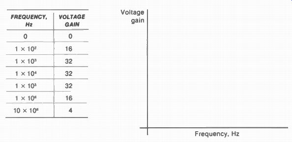
FIGURE 13-37 FOR PROBLEM 6.