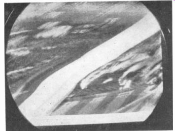
The automatic gain control (AGC) circuit varies the gain of the receiver according to signal strength. Less gain is needed for strong signals. Therefore, the AGC reduces the gain by changing the bias on the IF and rf stages to maintain a relatively constant level for the video detector output. Then the manual contrast control can be in the video amplifier for easy control of the contrast in the picture. The AGC bias is a dc voltage obtained by rectifying the video signal. Practically all receivers use AGC to prevent overload distortion. In Fig. 15-1 the overloaded picture has reversed black and-white values and is out of sync as a result of too much signal. The details of automatic gain control are explained in the following topics:
15-1 Requirements of the AGC circuit
15-2 Airplane flutter
15-3 AGC bias for tubes
15-4 AGC bias for transistors
15-5 Keying or gating pulses for the AGC rectifier
15-6 AGC circuits
15-7 Twin pentode for AGC and sync separator
15-8 AGC circuit in IC chip
15-9 Transistorized AGC gate and amplifier
15-10 Dc voltages in the AGC circuit
15-11 AGC adjustments
15-12 AGC troubles
FIGURE 15-1 OVERLOADED PICTURE. OUT OF SYNC WITH BLACK AND WHITE REVERSED.
THE DIAGONAL WHITE BAR IS HORIZONTAL BLANKING.
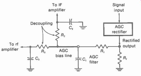
FIGURE 15-2 BASIC REQUIREMENTS OF THE AGC CIRCUIT.
15-1 Requirements of the AGC Circuit
The circuit of Fig. 15-2 illustrates how the AGC bias is used to reduce the receiver gain for strong signals. This idea is the same as automatic volume control (AVC) in radio receivers.
With AVC, the purpose is to have relatively constant volume for different signal levels at the antenna. With AGC for picture signal, the purpose is to have relatively constant contrast.
The stages connected to the AGC bias line are usually the rf amplifier with the first and second IF amplifiers. The last IF stage usually does not have AGC because varying the bias with a large signal swing can cause amplitude distortion.
AGC rectifier. In Fig. 15-2, the AGC rectifier stage changes the ac signal input to dc output for the AGC bias. More signal input produces more AGC bias: less signal means less bias. The ac input to the AGC rectifier can be either IF signal or video signal. The load resistor for the AGC rectifier is R1., which produces dc voltage output proportional to the ac signal input.
The AGC bias voltage has the polarity needed to reduce the gain of the IF and rf stages connected to the AGC line. For a vacuum tube amplifier the AGC bias is negative voltage applied to the control grid. The polarity of the AGC bias for transistors can be either positive or negative, depending on the circuit. In all cases, though, more signal produces more AGC bias to reduce the gain of the receiver.
AGC filter time constant. The rectified voltage across the AGC load resistor R _p must be filtered to remove the signal variations, since a steady dc voltage is needed for bias. This is the function of the AGC filter R,C, in Fig. 15-2. The RIC] time constant is about 0.2 S. A shorter time constant will not filter out the low-frequency variations in the rectified signal. Specifically, the vertical sync voltage can vary the AGC bias, which causes bend in the picture. Too long a time constant will not allow the AGC bias to change fast enough when the receiver is tuned to stations having different signal strengths. In addition, a long time constant will not remove the variations of picture intensity caused by fading of the signal when an airplane is flying nearby.
With tubes, a typical AGC filter has 0.1 µ.F for C, and 2 M-o for R,. For transistors, typical values are 20 k-o for R, and 10 uF for C. Note that 10 uF requires an electrolytic capacitor for the AGC filter in transistor circuits.
The AGC line. Each stage controlled by AGC has a return path to the AGC line for bias. Then the voltage on the AGC line varies the bias on the controlled stages. The filtered voltage across C, is the source of AGC bias to be distributed by the AGC line.
AGC decoupling filters. R2C2 and R,C, in Fig. 15-2 isolate each amplifier stage from the common AGC line. The isolation results from the series resistance of R2 or R„. This resistance reduces feedback between stages through the AGC filter capacitor as a common impedance.
However, each decoupling resistor need its bypass capacitor C2 or C3. The low capacitive reactance completes the ac signal path to ground in the amplifier circuit, without shorting the dc bias voltage from the AGC line.
AGC action. The AGC circuit provides relatively constant output voltage from the video detector, with wide variations in antenna signal. As an example, suppose that the rf tuner and IF section have an overall voltage gain of 100,000 for a weak antenna signal of 20 µV, resulting in 2 V of video signal at the detector output. Now assume that a much stronger antenna signal of 20 mV produces enough AGC bias to reduce the overall gain to 100. Note that 20 mV is 20,000 µV, or 0.02 V. The video detector output then is still 2 V. equal to the gain of 100 x 0.02 V. The AGC action reduced the voltage gain from 100,000 to 100. This ratio of 100,000/100 for voltage gain corresponds to 60 dB of AGC action in reducing the receiver gain.
Types of AGC circuits. The circuit in Fig. 15-2 is called simple AGC. In delayed AGC, there is no AGC bias at all unless the antenna signal is above a specific level, generally about 1 mV. The purpose is to prevent any reduction in gain by AGC action when the signal is weak. Usually, the AGC bias for the rf amplifier is delayed. The result is a better signal-to-noise ratio, for weak signal, to minimize snow in the picture.
In amplified AGC, the AGC voltage is increased so that a small change in signal level can produce a large change in bias. An amplifier for the AGC bias must have dc coupling for the input and output. Also, the polarity of the AGC bias can be inverted by the AGC amplifier. In keyed AGC or gated AGC, the AGC rectifier is keyed on by horizontal flyback pulses to con duct only during retrace time. The advantage is that noise pulses in the signal have little effect on the AGC bias voltage.
15-2 Airplane Flutter
This is a rise and fall of picture intensity, making the picture fade in and out, when airplanes are flying nearby. The cause is fading of the picture carrier signal as its amplitude increases and decreases because of the moving airplane.
For the carrier frequencies used in television broadcasting, the airplane is several wave lengths long and can act as an antenna, especially for the UHF channels. Since it is in the field of the radiated wave, the airplane intercepts some signal, current flows as on an antenna, and signal is reradiated. The reradiated signal may aid or oppose the original transmitted signal picked up by the receiving antenna. Further more, the phase relations change continuously as the airplane moves. The resultant fading occurs at a rate of about 10 to 25 fluctuations per second. This is the beat frequency between the direct and reflected signals.
In addition, the reradiated signal can produce a ghost in the picture. The sound may also be distorted and pulsate in volume. If the airplane is transmitting its own radio signal, this rf interference can cause diagonal bars in the picture.
The effects of fading in the antenna signal caused by airplane flutter can be practically eliminated by the picture AGC circuit, when the filter time constant is not too long. The required time constant is about 0.2 s or less.
15-3 AGC Bias for Tubes
The grid-plate transconductance (g„,) is reduced as the negative bias increases. As an example, g„, can be reduced from 10,000 µmhos for maximum gain to practically zero for minimum gain. For a pentode IF amplifier, the gain of the stage varies directly with the g,„ of the tube. As a result, the gain is reduced as the negative AGC bias makes the control-grid voltage more negative.
Series feed for AGC bias. In Fig. 15-3a, the AGC bias voltage is in series with the secondary L, of T, which supplies the IF signal to the control grid. Effectively, the AGC circuit is in the re turn path of L s to chassis ground. Then the AGC line has a dc path to the control grid to vary its bias. Since there is no grid current and L s has practically zero resistance, the AGC bias is the dc grid voltage. In addition, RA provides about 1 V of cathode bias, with its bypass CK. For the tuned circuit, the stray capacitance C, tunes with L s for resonance at the IF signal frequencies. In the decoupling filter, R, isolates the low side of the tuned circuit from the AGC line. The bypass C, returns L s to chassis ground. Then the IF signal has a return path through C, to cathode, without the series resistance of R. Shunt feed for AGC bias. In Fig. 15-3b, the AGC voltage is connected to the control grid through R, to supply grid bias. In this case, R, is used to prevent shorting the IF signal of the tuned circuit. Here C, couples the IF signal and blocks the AGC voltage from a dc short to ground through L s. Again, Rh and CK provide cathode voltage for a minimum bias.
Comparison of series and shunt feed. Note that with the shunt feed in Fig. 15-3b, R, in the AGC line is across the tuned circuit. Then R2 affects the damping and bandwidth for the IF signal. With the series feed in Fig. 15-3a, C, bypasses the AGC isolating resistor R _p but actually C, is part of the IF tuned circuit with L, and C,. An open in C, will result in practically no IF signal because of the high series resistance of R.
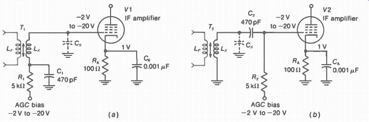
FIGURE 15-3 ROW CONTROL GRID IS RETURNED TO AGC LINE FOR NEGATIVE BIAS (a)
SERIES FEED (b) SHUNT FEED.
15- 4 AGC Bias for Transistors
For a transistor its beta (0) determines the gain, in a common-emitter (CE) amplifier. The beta is the ratio of a change in collector current to a change in base current, or 13 = ..1/(1.1/8. As an example, 13 may be 200 for maximum gain, which is reduced by AGC bias to practically zero for minimum gain. However, there are two opposite methods of using the AGC bias to reduce the beta. These are reverse AGC and forward AGC for transistors.
Reverse AGC. In this method, the transistor gain is decreased by reducing the forward bias at the base, toward cutoff. For instance, more negative AGC voltage at the base of an NPN transistor is reverse AGC, as the positive forward base bias is reduced. Remember that a transistor is cut off with zero forward voltage. As the base-emitter bias approaches cutoff, the changes in I_C. are smaller for changes in I_B, reducing the beta.
Actually, reverse AGC corresponds to the idea of increasing the negative grid bias toward cutoff for a tube. However, the polarity for reverse AGC bias can be either negative or positive to approach cutoff for transistors. Reverse AGC voltage is negative for the base of an NPN transistor but positive for a PNP transistor.
Forward AGC. In this method, tie transistor gain is decreased by increasing the forward bias at the base, toward saturation. For instance, more positive voltage at the base of an NPN transistor is forward AGC. It should be noted that rf ard IF stages controlled by forward AGC generally use special transistors with the required beta characteristic for less gain with more forward bias. This is accomplished by a special shape in the emitter construction.
The polarity of forward AGC at the base can be positive for NPN transistors or negative for PNP transistors. Practically all small-signal transistors are NPN, however, so that we can think of positive voltage at the base as forward AGC in a CE amplifier. Furthermore, forward AGC is generally used more than reverse AGC. The reason is that operation near cutoff with reverse AGC makes the receiver more susceptible to overload and cross-modulation distortion on strong signals.
Forward AGC bias with series feed. See the IF amplifier in Fig. 15-4. When the AGC voltage becomes more positive, it increases the forward bias at the base of the NPN transistor. The RR2 voltage divider provides a fixed positive base bias, from the collector supply V_CC. R3 is the AGC decoupling resistor, with its bypass C. The dc voltage at the junction of R1, R2, and R3 is the base voltage, as the IF transformer has very little resistance. This 2.6 V at the base is the dc voltage to chassis ground. Also, the 2 Vat the emitter is to ground. This voltage is the IR drop across RE produced by the emitter current.
Therefore, the actual base-emitter bias is 2.6 - 2 = 0.6V as a typical forward voltage for an NPN silicon transistor. When the AGC voltage increases with more signal, the result is more forward bias toward saturation to decrease the gain.
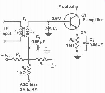
FIGURE 15-4----HOW BASE OF NPN TRANSISTOR IS RE TURNED TO AGC LINE BIAS VOLTAGE
HERE IS POSITIVE FOR FORWARD AGC.
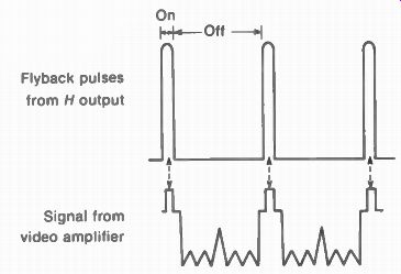
FIGURE 15-5----KEYING PULSES AT HORIZONTAL SYNC RATE FOR AGC CIRCUIT
Typical changes in AGC bias. When the AGC bias changes, the actual change in base voltage ( V B) is generally less than 0.1 V. However, the change in base current (I_B) can be appreciable.
As an example, a change in V E from 0.6 to 0.65 V can change I E from 100 to 200 µA. Furthermore, this increase in I_B raises the average dc collector current (I_C.) and emitter current (I_E). The change in i t; can be seen by measuring the emitter dc voltage across RE. Similarly, when the collector circuit has a series decoupling resistor, its dc voltage can be measured to see the change in I_C.
15-5 Keying or Gating Pulses for the AGC Rectifier
Most AGC circuits use flyback pulses from the horizontal output circuit for keying or gating the AGC rectifier into conduction. The video signal is also coupled into the rectifier to provide AGC voltage proportional to signal strength. However, the AGC stage is generally biased to cutoff so that it conducts only for the short time the pulse is applied. Then the signal is rectified only when the blanking and sync pulses are on. As shown in Fig. 15-5, the time of the flyback pulses corresponds to the time of sync and blanking, assuming the picture is in sync. The gating function means that both inputs must be on at the same time to produce output.
The advantage of keyed AGC is that the rectified voltage is free from noise pulses that can occur between the horizontal sync pulses. In addition, there is no error in AGC bias from the vertical sync pulses, because their greater width is not measured by the keyed AGC rectifier. Therefore, the time constant of the AGC filter can be shorter for a faster response to airplane flutter. Finally, the AGC rectifier can be a peak rectifier, producing dc output only for the sync peaks of the ac signal input. This factor helps in preventing the AGC bias from changing with different dc levels of scene brightness in the video signal. The AGC bias should vary only with the strength of rf carrier signal on the antenna.
Keying a triode AGC tube. See Fig. 15-6. Video signal is directly coupled from the video output circuit to the grid of the AGC tube. The dc voltage here is ±115 V because of the dc coupling. The grid-cathode bias is 115V- 140 V = -25 V. Without signal, then, the - 25 V biases AGC tube beyond cutoff. Furthermore, the plate does not have any positive dc supply voltage.
However, the horizontal flyback pulses drive the plate positive during the sync pulse time. Therefore, the tube conducts plate current when the video signal with 80-V peak-to-peak amplitude makes the grid more positive than cutoff. The horizontal sync pulses at the positive peak of the video signal drive the grid voltage to zero so that the tube can conduct as the plate is pulsed positive at this time.
The plate circuit of the AGC tube in Fig. 15-6 must produce negative voltage for the AGC bias line. This is why there is no B+ voltage for the plate. Instead, the plate is pulsed positive by the flyback pulses with a peak amplitude of 400 V to produce plate current. Furthermore, the plate current produces negative AGC voltage by charging C2. When plate current flows, it charges C, with the plate side negative. The path for charging current includes the cathode to-plate circuit in the tube, C, and the AGC winding in the horizontal output transformer, with electron flow returning to the cathode.
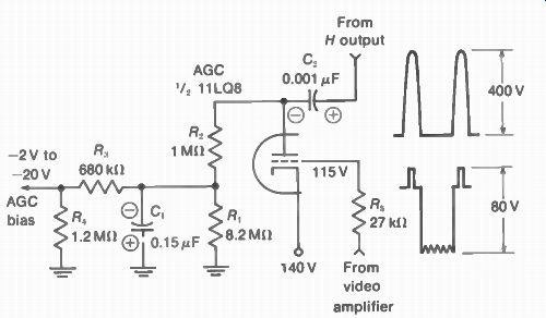
FIGURE 15-6 HORIZONTAL FLYBACK PULSES APPLIED TO PLATE OF TRIODE FOR KEYED
AGC
Between pulses, when the tube does not conduct, C2 can discharge through R2 to charge the AGC filter C1. The time constant of the AGC filter with C1, R1, R3, and R4 is much longer than the 63.5 u-s between pulses. Therefore, the voltage across C, is a relatively steady dc voltage for the AGC bias.
The function of R5 in Fig. 15-6 is decoupling to isolate the AGC tube from the video amplifier supplying the signal input. R, in the plate circuit isolates the AGC circuit from the horizontal output circuit supplying the flyback pulses.
R1 and C1 form the AGC filter. Finally, R3 and R4 form a voltage divider, with the voltage across R4 the filtered AGC voltage for the bias line.
Keying a transistor AGC stage. See Fig. 15-7.
The idea of keyed AGC here is the same as for the triode in Fig. 15-6, but smaller voltage amplitudes are used for transistors. The collector is pulsed, instead of the plate. Furthermore, the required polarity of the flyback pulses is negative for the PNP transistor in Fig. 15-7. Note that the base voltage is actually past cutoff. The base-emitter voltage of 1.8 - 1.6 = 0.2 V is actually a small reverse bias because it is positive voltage for the base of a PNP transistor.
However, the video signal with 3-V peak to-peak amplitude drives the transistor into conduction when the collector is pulsed on. The video signal input here has negative sync polarity for the base of the PNP transistor. Then the negative sync voltage is in the forward direction to produce collector current. The polarity of the flyback pulses is also negative to be reverse collector voltage for a PNP transistor.
In Fig. 15-7, the 100-V flyback pulse is supplied by L1, which is a separate winding on the horizontal output transformer. With this AGC winding, either polarity of flyback pulses can easily be obtained. In addition, the separate AGC winding isolates the AGC circuit from the horizontal output circuit. This method of obtaining the flyback pulses can be used with transistors or tubes.
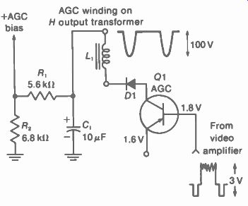
FIGURE 15-7 HORIZONTAL KEYING PULSES AT COLLEC TOR OF AGC STAGE. NEGATIVE
PULSES ARE USED HERE FOR PNP TRANSISTOR
The diode D1 is necessary for isolation in the transistor AGC stage because the AGC bias voltage is the opposite polarity from the required collector voltage. In Fig. 15-7, the AGC voltage is positive, which would put forward voltage on the collector of the PNP transistor. However, D1 isolates the positive AGC voltage. Remember that the arrow on the diode is the anode, while the bar is the cathode. Therefore, D1 can couple the negative flyback pulses from cathode to anode for the collector. However, the positive AGC voltage cannot produce current from cathode to anode in the diode. As a result, D1 prevents C1 from discharging through the AGC transistor.
It may be interesting to note that an NPN transistor could be used in Fig. 15-7. Then all the polarities would be reversed. The flyback pulses at the collector would be positive. The video signal would have positive sync polarity. The base-emitter voltage for reverse bias would be negative. Finally, the AGC voltage across C, in the collector circuit would be negative, with an NPN transistor for the AGC stage.
15-6 AGC Circuits
Typical circuits are shown in Figs. 15-6 to 15-11. Either the modulated picture IF carrier signal or the detected video signal can be rectified by the AGC stage to supply the AGC bias voltage. In most receivers, however, the AGC circuit uses signal from the video amplifier because the higher signal level allows more control by the AGC bias.
With video signal input, it must have dc coupling to the AGC stage in order to preserve the dc component. Then the pedestals of the video signal are in line so that a peak rectifier can measure the sync voltage level to measure the carrier strength correctly.
It should be noted that the picture IF signal has the dc component of the video signal in the modulation. The simplest method of using the IF signal for AGC is to take the AGC bias from the video detector load resistor, as shown in Fig. 15-8. With integrated circuits, the AGC circuit can be part of the IC chip for the IF amplifier.
The stages controlled by AGC bias are generally the rf amplifier in the tuner and one or two IF stages. The last IF stage usually does not have AGC bias. This IF stage has a relatively high signal amplitude, which can easily be distorted by a change in bias. Also, the effect of the AGC is proportional to signal gain from the controlled stage to the AGC rectifier. Therefore, AGC on the earlier stages has more control on the overall receiver gain.
Separate rf and IF bias lines. There are usually separate bias lines for the IF amplifier and to the rf amplifier because the needs are different.
With weak signal, the rf bias should allow maximum gain, for a good signal-to-noise ratio and minimum snow in the picture. The snow is produced by internal noise generated in the rf amplifier and mixer stages. The only way to eliminate the snow is to have a large enough signal from the rf tuner, before the IF amplification.
With very strong signal, cross modulation can be produced in the mixer stage, because it is a nonlinear amplifier. Cross modulation results when the modulation of a weak signal is impressed on the carrier of a strong signal. The result of cross modulation is two signals that produce two pictures on the screen. Therefore, with a strong signal the AGC bias must reduce the gain for the rf tuner to minimum, in order to prevent cross modulation in the mixer.
These requirements for rf and IF gain can be summarized as follows:
1. Weak signal--up to about 0.1 mV. Rf gain is maximum for minimum snow. IF gain is the amount needed for constant video detector output.
2. Normal signal--about 0.1 to 100 mV. A typical value is 1 mV. Rf and IF gain are reduced to provide constant output from the video detector.
3. Very strong signal--above 100 mV. Rf gain is minimum to prevent cross modulation, and IF gain is minimum to maintain constant video detector output.
AGC delay. This delay is in voltage, not in time.
The purpose is to hold off any AGC bias until the signal is strong enough for a picture without snow. The method is to keep the delay stage cut off until a specific amount of AGC voltage is available. Usually, when an AGC delay stage is used, it is in the rf bias line for the tuner.
Bias clamp. This means clamping, or holding, the AGC bias at a specific voltage level. Generally, a diode is used for the clamp circuit. When the diode conducts, it connects the AGC bias line to a fixed voltage source, preventing any increase in the AGC bias.
Noise inverter. Also called a noise gate, this circuit inverts the polarity of noise pulses by reversing the polarity of its video signal. The purpose is to cancel noise pulses in the video signal to the AGC stage. The noise inverter is also used for the sync separator circuit. As an example, the circuit in Fig. 15-9 combines the AGC stage and sync separator, with a noise inverter circuit common to both.
Triode AGC circuits. Referring back to the triode tube in Fig. 15-6 and the transistor in Fig. 15-7, these circuits illustrate a common type of keyed AGC. This stage is generally called the AGC gate or AGC keyer. The gating means that the stage is keyed on to conduct only during the horizontal flyback pulses.
AGC bias from the video detector output. Refer to Fig. 15-8. Actually, D1 is the video detector, but the dc output voltage across the load resistor RI , is proportional to signal strength. Therefore, the voltage across R, . is filtered and used for AGC bias. R, and R, isolate the AGC filter capacitors C, and C, from the detector load R1,. The combination of video detector and AGC rectifier is seldom used because the diode cannot be a peak rectifier to measure signal strength correctly. Also, the video detector cannot be keyed for the AGC function. However, this circuit illustrates a method of rectifying the IF signal for the AGC voltage.
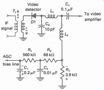
FIGURE 15-8 AGC BIAS FROM VIDEO DETECTOR LOAD RESISTOR R,
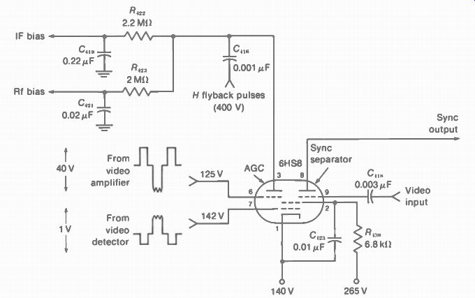
FIGURE 15-9 TWIN PENTODE TUBE FOR AGC AND SYNC SEPARATOR. (FROM ADMIRAL CHASSIS)
15-7 Twin Pentode for AGC and Sync Separator
See Fig. 15-9. The special tube for this application has one cathode and one screen grid common to both sharp-cutoff pentodes. Also common is the first control-grid pin 7, which serves as a noise gate. The AGC stage at the left has a separate grid connection at pin 6 for video signal input, with the AGC output at plate pin 3.
The pentode at the right has its own grid pin 9 for video input and plate pin 8 for sync output.
This sync separator is explained in more detail with Fig. 16-29 in Section 16 on Sync Circuits. The twin pentode tubes generally used for this combined sync and AGC circuit are the 4HS8, 6HS8, 3BU8, and 6BU8.
The plate of the AGC section is keyed into conduction by horizontal flyback pulses coupled through C4, 6. When plate current flows, it charges C.„„ through R„, and C _p, through R„ _p. The plate side is negative for negative AGC bias to the rf and IF amplifier tubes. Separate bias lines are used to isolate the rf and IF stages.
The AGC grid at pin 6 has the dc voltage of 125 V because of direct coupling from the video amplifier. The cathode is at 140 V. Therefore the grid-cathode voltage equals 125 -140 = --15 V. This bias is more negative than cutoff. With video signal input of 40 V peak to-peak, though, the positive sync peaks produce plate current when the plate is keyed on by horizontal flyback pulses. These keying pulses have a peak amplitude of 400 V. As a result, the AGC output in the plate circuit is a measure of signal strength.
The noise inverter grid at pin 7 has composite video signal of only 1 V, with negative sync polarity. Note this is the opposite of the sync polarity at the AGC grid pin 6. The dc voltage at the noise inverter grid is set 2 V more positive than the cathode, so that the negative sync cannot cut off plate current. However, noise pulses of high amplitude can drive the grid more negative than cutoff. Then noise pulses in the video signal cannot produce output in either the AGC stage or the sync separator.
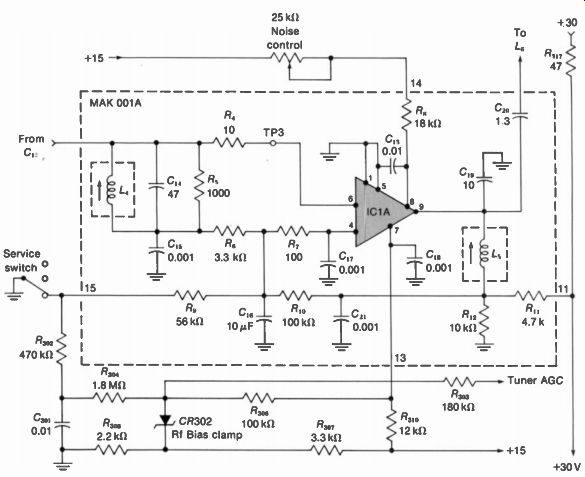
FIGURE 15-10 INTEGRATED CIRCUIT FOR AGC STAGE. (FROM RCA CHASSIS CTC 49)
15-8 AGC Circuit in IC Chip
See Fig. 15-10 [...] AGC circuit.
The IC1B half, not shown, has the last IF stage and video preamplifier, with the input of horizontal flyback pulses needed for the AGC. We can consider pin 4 as the collector of an AGC transistor in the IC chip, The 100-o R9 is the load resistor in series with the 56-k-o R, to ground, through the service switch at the left.
The 10-µF C10 is the AGC filter capacitor. Collector supply voltage is obtained through the 100-k-o R10.
The series feed for the IF AGC is from pin 4, through 137 and R6, to the low end of the IF coil L4 and back into the IC chip through R4 to terminal 6 for the IF input. The rf AGC line is out at pin 7 of the chip, through R306 , and R303 to the rf tuner. Note that CR302 is a zener diode, with the function of clamping the rf bias voltage. The noise control at the top of the diagram adjusts the rf AGC bias for minimum snow with weak signal.
The normal-service switch is shown in the position for a normal picture with ground at the junction of R9 and R302. When the ground point is removed, the AGC bias cuts off the IF amplifier for a clean raster without snow. This service position is for purity adjustments on the color picture tube.
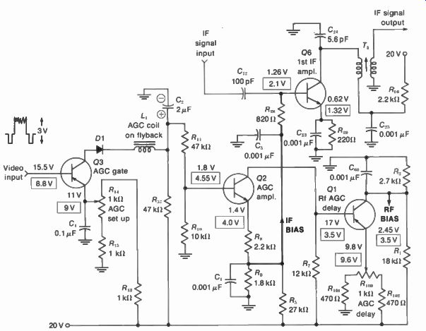
FIGURE 15-11 TRANSISTORIZED AGC GATE AND AMPLIFIER WITH DELAY STAGE FOR RF
BIAS DC VOLTAGES IN BOXES ARE WITH SIGNAL INPUT TO RECEIVER (FROM MOTOROLA
CHASSIS CTV5-S5)
15-9 Transistorized AGC Gate and Amplifier
Figure 15-11 shows the AGC circuit of a transistorized receiver, with the details of AGC amplification and delay. Starting with the AGC gate Q3 at the left, the video input signal is rectified to produce AGC output voltage across the filter capacitor C2. Note that Q3 is a PNP transistor.
Then the video input signal has negative sync polarity, the keying pulses are negative at the collector, and the AGC output voltage is positive.
The AGC bias voltage from Q3 is dc coupled to the base of the AGC amplifier Q2.
This is an NPN transistor. The positive input at the base is inverted to negative voltage at the collector output for the next stage Q1. However, the AGC voltage at the emitter of D2 has the same positive polarity as the input, since the emitter voltage follows the base voltage. This positive AGC voltage at the junction of R„ and R, in the emitter circuit of Q2 is used for AGC bias on the IF amplifier Q6. Since 06 is an NPN transistor, the positive bias at its base is for ward AGC. The AGC amplifier D2 also serves as a buffer stage to separate the IF bias line at the emitter of Q2 from the rf bias line at the collector of Q1. The output at the collector of Q2 is negative AGC voltage to the base of the rf AGC delay stage Q1. Note that Q1 is a PNP transistor. For either PNP or NPN types, though, the polarity at the collector is inverted from the input at the base. Therefore, the negative AGC bias into D2 is inverted to positive at the collector for the rf bias line. The AGC delay control R100 in the emitter circuit is set to keep this stage cut off until the signal can produce enough AGC voltage at the base to make Q1 conduct.
The AGC gate circuit. Now we can consider the function of each component in Fig. 15-11.
For the AGC gate Q3, which produces the AGC voltage, R57 is the collector load resistor in series with the AGC coil L, and D1 as a blocking diode.
L1 supplies negative flyback pulses with a peak amplitude of 40 V from the horizontal output transformer. The 2-µ.F electrolytic capacitor C2 is the AGC filter with R10 and R11. The positive AGC voltage is blocked by D1 from the collector of Q3, which needs negative collector voltage because it is a PNP transistor. Most important, the diode D1 prevents the AGC filter capacitor C, from discharging through the AGC transistor Q3. In the emitter circuit of Q3, the voltage divider of R13 R 14, and R15 provides the emitter bias. R„ sets this bias for the desired amount of AGC voltage output. C, is an rf bypass capacitor.
The AGC amplifier circuit. For the AGC amplifier Q2, the collector load resistor is R7. In the emitter circuit, the voltage across R, supplies the AGC bias voltage for the IF bias line. A1 though R, is part of a voltage divider with R5 from the 20-V supply, the voltage across R, varies with the emitter current through R, in series with R. More conduction in Q2 produces more AGC voltage across R„, with positive polarity in the emitter circuit.
The AGC delay stage. The negative AGC voltage at the collector of D2 is dc-coupled to the rf AGC delay stage Q1. In the collector circuit of Q1, the voltage divider of R, and R, provides collector voltage from the 20-V supply. C,„ is an rf bypass capacitor. The positive AGC voltage at the collector feeds the rf bias line to the tuner. In the emitter circuit of Q1, the point of conduction is set by the AGC delay control R _p,. This adjusts the emitter voltage provided by the voltage divider of R1442 , R100 , and R,„, from the 20-V supply line at the bottom of the diagram.
15-10 DC Voltages in the AGC Circuit
The AGC bias itself is a dc voltage, and the entire AGC circuit is a network of dc values from input to output.
Dc level of the video signal. The video signal to be rectified must have its dc component.
Otherwise, the AGC bias would vary with scene brightness, instead of indicating the strength of carrier signal at the antenna. For this reason, the video signal has dc coupling, without any series capacitors, from the video amplifier to the AGC stage.
Dc voltage on the AGC bias line. The dc bias on the AGC line cannot have any series capacitors in the feed line to the rf and IF controlled stages. When shunt feed is used for the tuned amplifier, this stage has a series capacitor to couple the signal and block the AGC bias from shorting through the rf or IF coil. With series feed for the AGC bias, the bypass capacitor in the decoupling filter completes the tuned circuit for the rf or IF stage, without shorting the dc voltage on the bias line.
DC voltages in the AGC amplifier. When an AGC amplifier is used, this stage must be a dc amplifier, without any series coupling capacitors. The AGC amplifier can provide a reversal of polarity for the AGC bias, in addition to the amplification. Also, the AGC amplifier often serves as a buffer between AGC takeoff points in the output and input for rf and IF bias voltages.
DC coupling in the controlled stages. In many circuits the AGC bias is on an rf or IF amplifier that has direct coupling to the next stage. Then the dc connection puts the AGC on both amplifiers. In fact, the AGC bias is amplified and usually inverted for the next amplifier.
Typical AGC voltages for transistors. We can use Fig. 15-11 to see the dc voltages in a transistorized AGC circuit. For Q3 the base is at 8.8 V with signal. Note that the values in the boxes are with signal. The 8.8 V at the base of Q3 is from the dc coupling to the video amplifier. The emitter of Q3 is at 9 V, from the 20-V supply. The actual base-emitter bias V„,.: then is 8.8 V - 9.0 V, which equals -0.2 V. This value is normal forward bias on the PNP germanium transistor for Q3.
At the base of Q2, the AGC bias voltage is 4.55 V. The emitter is at 4.0 V. Then V_RE is 4.55 - 4.0 = 0.55 V. This is normal forward bias for the silicon NPN transistor for Q2.
Notice that the emitter voltage of Q2 changes from 1.4 V without signal to 4.0 V with signal. This change of 4.0 V - 1.4 V is an increase of 2.6 V in positive AGC bias.
At the rf AGC delay stage Q1, note that the collector-emitter voltage 141. : is actually negative for this PNP transistor, although the collector to-ground voltage is positive. For the voltage values with signal, V rE is 3.5 - 9.6 V = -6.1 V. The positive 3.5 V at the collector provides forward AGC voltage for the rf amplifier on the tuner.
15-11 AGC Adjustments
When the receiver has controls for adjusting the amount of AGC action, they have a big effect on the picture and sound because the AGC bias sets the overall rf and IF gain. These controls are provided to adjust the amount of AGC for strong signals or weak signals in different areas.
With tubes, the AGC level control usually can be varied to cut off the picture and sound at one end or produce an overloaded picture (Fig. 15-1) at the opposite extreme. This control can be set by adjusting for an overloaded picture, on the strongest station, and then backing off a little for a normal picture with good contrast.
With transistors, the AGC level control may not be able to produce an overloaded picture. The corresponding idea is to adjust for maximum snow in the picture and then to back off a little. To set the AGC level exactly, the service notes for the receiver give a specific value of AGC bias needed for the signal level of 1 V peak to-peak out of the video detector.
When the receiver has two AGC adjustments, usually one is for AGC level and the other for rf delay. The AGC level is adjusted with a strong signal, just below overload. However, the rf delay is adjusted with a weak signal, for the best signal-to-noise ratio with minimum snow in the picture.
15-12 AGC Troubles
The AGC circuit is a common cause of troubles in the picture, while the raster is normal. Too much AGC bias reduces the receiver gain, causing a weak picture. This weak picture is without snow. A weak antenna signal can also produce a weak picture but with the snow caused by a poor signal-to-noise ratio in the rf tuner.
When the AGC bias is great enough to cut off an rf or IF amplifier, the result is no picture, with a blank raster. The sound is also cut off because of the intercarrier sound circuit. Troubles in the AGC amplifier can cause too much AGC bias.
For the opposite case, when there is not enough AGC bias, the receiver has too much gain. Then the rf mixer, an IF stage, or the video amplifier can have too much signal for the bias.
The result is overload distortion. This term just means that the amplifier has amplitude distortion caused by too much signal input, by too little bias, or by both.
Overloaded picture. See Fig. 15-1. This picture has reversed black-and-white values and is out of sync. The white diagonal bar is horizontal blanking, which should be black and at the side.
Usually, the picture will roll vertically also. The picture is out of sync horizontally and vertically because the sync pulses are either compressed or lost completely with the severe amplitude distortion.
The reversed black-and-white values are caused by reversal of the polarity of modulation for the video signal as a result of rectification in an overloaded amplifier, which is usually the last IF stage. The buzz in the sound is caused by the vertical blanking pulses of the video signal modulating the sound signal in an overloaded IF stage common to both picture and sound.
The AGC troubles of too much or too little bias are summarized in Table 15-1.
It should be noted that too little AGC bias can also cause high contrast and bend in the picture, just before the point of a reversed picture out of sync. Furthermore, if the receiver tends to overload on normal signal levels but has a normal picture with a very weak signal, this can be a clue to the trouble of not enough AGC bias.
----------

TABLE 15-1 AGC TROUBLES
TROUBLE EFFECT
Too little AGC bias Overload distortion, with reversed picture out of sync and buzz in the sound.
Too much AGC bias No sound and no picture, with normal raster.
------------
Localizing picture troubles to the AGC circuit. A test of the AGC action can be made by shorting the AGC bias to ground, temporarily, either on the AGC bias line or the AGC filter capacitor. The result is zero AGC bias. The result of zero AGC bias with tubes is an over loaded picture. Similarly, with reverse AGC on transistors the result is a stronger picture or overload. With forward AGC on transistors, though, the result of zero AGC bias is less picture or no picture. In all cases, though, shorting the AGC bias should have a big effect on the picture. If there is no effect, the trouble is either a short in the AGC line or a defect in the rf and IF amplifiers.
Battery bias box. A more general method of localizing troubles to the AGC circuit requires the use of a bias box, as shown in Fig. 15-12.
This provides an adjustable bias voltage to take the place of the AGC bias. Connect one output lead directly to the AGC line and the opposite lead to chassis ground. The low resistance of the battery effectively shorts the high-resistance AGC circuit, so that it need not be disconnected.
If the picture and sound are normal when the battery supplies the bias, but not with the AGC bias, the trouble must be in the AGC circuit. The bias box is also useful for supplying the fixed bias that is necessary in rf and IF alignment.
The polarity of the bias box is shown with negative output in Fig. 15-12, for negative grid bias on tubes. With transistors, though, the required polarity may be either negative or positive. For positive bias voltage, connect the positive output lead to the AGC line and ground the negative lead.
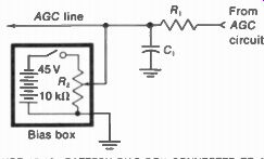
FIGURE 15-12 BATTERY BIAS BOX CONNECTED TO AGC LINE FOR MANUAL CONTROL OF
BIAS.
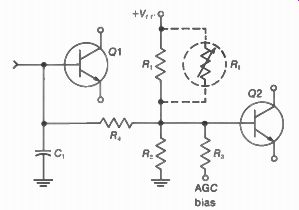
FIGURE 15-13 VARYING THE TRANSISTOR IF BIAS MANUALLY WITH R. TO CHECK FOR
AGC TROUBLE.
Manual control of bias line for transistors. Figure 15-13 shows Q1 and Q2 dc coupled at the base to share the AGC bias. The function of the AGC voltage here is to vary the positive base bias. Positive forward bias at the base is provided by the R, R„, divider from the supply voltage V cc . If you connect a variable resistor R, of about 25 kit across R _p then R, can be used to control the bias manually This method does not require a bias box. If a normal picture can be obtained with R, but not with the AGC alone, this shows trouble in the AGC bias.
AGC filter capacitor. This capacitor in transistorized AGC circuits is an electrolytic one. A short causes the trouble of zero AGC bias. If the capacitor is leaky, with insufficient capacitance, the result will be too little AGC bias.
AGC blocking diode. An example of an AGC blocking diode is D1 in Fig. 15-7 for transistor Q3. If the diode is open, there will be no AGC voltage on the AGC bias line. If the diode shorts, there will be forward voltage on the AGC stage, making it conduct too much. The result can be either a short on the AGC line or the AGC transistor becoming defective.
Troubles In the AGC decoupling filters. With series feed for the AGC line to the rf or IF amplifier, the bypass capacitor in the decoupling filter is part of the tuned circuit for signal. An example is C, in Fig. 15-4. If C, is open, the tuned circuit with L s for IF signal will be practically open for ac signal, because of the resistance of R,. The result is very weak signal. If C, is shorted, the AGC bias on Q1 will be zero.
SUMMARY
1. The AGC circuit rectifies the signal to produce dc bias proportional to signal strength so that the AGC bias can control receiver gain. More signal produces more AGC bias to reduce the rf and IF gain for constant output at the video detector.
2. The AGC filter removes the signal frequencies to make the AGC voltage a dc bias. A typical filter time constant is 0.2 s. An electrolytic capacitor of 5 to 10 uF is generally used for the AGC filter in transistor circuits.
3. The filtered AGC bias is distributed by the AGC line, through an RC decoupling filter to each controlled stage.
4. In delayed AGC, no bias is produced until the signal is strong enough to over come the delay voltage on the AGC stage. The result is a better signal-to-noise ratio for less snow with weak signals. The rf amplifier usually has delayed AGC.
5. In keyed or gated AGC, the AGC stage is pulsed into conduction by horizontal flyback pulses. This stage is generally called the AGC keyer or AGC gate. The polarity of the flyback pulses is positive on tubes and NPN transistors, or negative for PNP transistors, at the collector.
6. A transistor for the AGC stage needs a diode to block the AGC voltage from its collector and to prevent the AGC filter capacitor from discharging through the AGC transistor.
7. For forward AGC on transistors, the forward voltage at the base is increased by the AGC bias. On an NPN transistor, forward AGC voltage at the base has positive polarity.
8. For reverse AGC on transistors, the forward voltage at the base is reduced toward cutoff by the AGC bias to reduce the amplifier gain. On an NPN transistor, reverse AGC voltage at the base has negative polarity.
9. For AGC on tubes, the bias makes the control grid more negative to reduce the amplifier gain.
10. Too little AGC bias can cause an overloaded picture and 60-Hz buzz in the sound. The overloaded picture (Fig. 15-1) has reversed black-and-white values and is out of sync.
11. Too much AGC bias results in no picture and sound, caused by cutoff in one or more of the rf and IF amplifiers.
12. The AGC level control sets the amount of bias for the rf and IF stages controlled by AGC bias. When the AGC control can produce an overloaded picture, set the adjustment just below the point of overload on the strongest signal. If there is no overload, set the AGC for minimum snow on the weakest signal.
Self-Examination (Answers at back of guide)
Answer True or False.
1. The AGC bias increases with more picture carrier signal at the antenna.
2. The AGC filter removes video signal variations from the dc bias voltage.
3. A keyed AGC stage conducts only during the time of the H flyback pulses.
4. With a PNP transistor for the keyed AGC stage, the H flyback pulses have negative polarity at the collector.
5. With a PNP transistor for the keyed AGC stage, the AGC voltage output at the collector has positive polarity.
6. For forward AGC, the bias is negative at the base of an NPN amplifier.
7. For reverse AGC, the bias is negative at the base of an NPN amplifier.
8. For AGC bias on tubes, the AGC bias is negative at the control grid.
9. Too much AGC bias can cause an overloaded picture with buzz in the sound.
10. The problem of airplane flutter is helped by a shorter time constant for the AGC filter.
11. A voltage gain of 10,000 equals approximately 1,000 dB. 12. With positive AGC voltage into the base of an AGC amplifier, the AGC bias output at the collector has negative polarity.
Essay Questions
1. What is the main advantage of AGC for the picture signal?
2. In an AGC circuit, give the function of (a) AGC rectifier; (b) AGC filter; (c) AGC line; (d) AGC decoupling filters.
3. Why is the video signal coupled to the AGC stage without any series blocking capacitors?
4. What signal stages are usually controlled by the AGC bias?
5. What is the purpose of delayed AGC?
6. When the carrier signal level increases, what is the effect on the amount of negative AGC bias on tubes? Give the effect on receiver gain.
7. Give the polarity required for the following examples of AGC bias at the base of a transistor IF amplifier: (a) forward AGC with an NPN transistor; (b) reverse AGC with an NPN transistor; (c) forward AGC with a PNP transistor; (d) reverse AGC with a PNP transistor.
8. Show how to connect a battery bias box to the AGC line, for the case of forward AGC on NPN amplifier stages.
9. What is the advantage of keyed AGC?
10. What two input voltages are necessary for a keyed AGC stage to conduct?
11. Give the polarity of flyback pulses needed for (a) plate of AGC tube; (b) collector of PNP AGC stage; (c) collector of NPN AGC stage.
12. What are two characteristics of an overloaded picture?
13. With an overloaded picture, why is there usually buzz in the sound?
14. Describe briefly why zero AGC bias can cause an overloaded picture.
15. Describe briefly why too much AGC bias can cause no picture and no sound.
16. Describe how to adjust the AGC level control, for the case where it can produce an overloaded picture.
17. What is meant by snow in the picture? What is the main cause?
18. Refer to the dc voltages in the AGC stage in Fig. 15-9. Give the values for: (a) pin 1, pin 7, and pin 6 to ground; (b) grid-cathode bias at pin 7, with polarity; (c) grid cathode bias at pin 6, with polarity.
19. Give the function of each component for the AGC stage in Fig. 15-7.
20. In Fig. 15-7, give the dc values for (a) V E to ground; (b) V„ to ground; (c) V BE with polarity.
Problems
1. Calculate the time constant in seconds for the following RC combinations: (a) 2 M-o and 0.1 µF; (b) 20 M-o and 10 µF.
2. What value of R is needed with C of 5 µF for a time constant of 0.1 s?
3. A signal voltage of 1,000 µV at the antenna is amplified to 2-V output from the video detector. How much is the overall voltage gain?
4. How much is the dB gain for Problem 3? (Decibels are explained in Sec. 26-7.)