The color section in the television receiver amplifies the 3.58-MHz chroma (C) signal, detects the modulation, and provides red, green, and blue video signals for the three guns of the tricolor picture tube. The color circuits are usually on a plug-in board, as shown in Fig. 17-1. In addition, the luminance (y) signal is amplified to form a mono chrome picture on the raster. Then the color information can be superimposed on the black-and-white picture. The theory of color television and block diagrams of color receivers are described in Chaps. 8 and 9, but here we analyze the basic circuits in the color section. Automatic circuits that are generally used to obtain the best color picture are described in the next SECTION. The fundamental requirements for color can be seen from this list of circuits:
17-1 Signals for the color picture
17-2 The video preamplifier stage
17-3 The Y-channel video amplifier
17-4 Chroma bandpass amplifiers
17-5 The burst amplifier stage
17-6 Color oscillator and synchronization
17-7 AFPC alignment
17-8 Chroma demodulators
17-9 Matrixing the Y video and color video signals
17-10 Video amplifiers for color
17-11 The blanker stage
17-12 Troubles in the color circuits
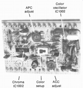
FIGURE 17-1 COLOR CIRCUITS ON PLUG-IN BOARD. WIDTH IS 5 IN. (ZENITH CORPORATION)
17-1 Signals for the Color Picture
The colorplexed composite video signal out of the video detector stage includes the Y signal for luminance multiplexed with the 3.58-MHz C signal for color information. The modulated C signal is amplified in the chroma bandpass amplifier. This stage is tuned to 3.58 MHz with a total bandwidth of 1 MHz. The amplitude of C signal determines color saturation. Its phase angle determines the hue or tint, with respect to the reference of burst phase.
The colorplexed composite video signal also includes the burst of 8 to 11 cycles of 3.58 MHz on the back porch of each horizontal blanking pulse. This burst is the reference phase for color synchronization, to determine hue or tint.
The phase of burst is yellow-green, exactly 180° opposite from B - Y phase. In the color circuits, the burst is separated and amplified by the burst amplifier stage. Then the burst is used for automatic frequency and phase control (AFPC) on the 3.58-MHz color oscillator.
The color oscillator regenerates the sup pressed subcarrier to supply 3.58-MHz cw for the synchronous demodulators. They also have C signal input. Then each demodulator detects the phase of C signal that is synchronous with the phase of its oscillator cw input.
The detected color signals generally have the phase of R - Y and B - Y video, which are then combined to form G - Y video. These color-difference signals are matrixed with the Y signal to form the red, green, and blue video signals for the picture tube.
Frequencies for chroma and color video. It is important to note the difference between modulated chroma signal at 3.58 MHz and the detected color video signals with a bandwidth of 0 to 0.5 MHz. In brief, 3.58 MHz is the frequency for color before demodulation of the chroma signal. Actually, 3.58 MHz is the color IF of the receiver, and a chroma bandpass stage is a color IF amplifier. The bandwidth of these tuned stages in the receiver is ±0.5 MHz.
After demodulation of the 3.58-MHz C signal, the color video signals have the baseband frequencies of 0 to 0.5 MHz. This bandwidth of 0.5 MHz for the detected color video applies to R - Y, B - Y, G - Y, R, G, and B signals.
All colors are in the 3.58-MHz chroma signal. The purpose of broadcasting the 3.58-MHz C signal is to have all the color information in one modulated signal. Amplifier stages for chroma signal affect all colors, therefore. These include red, green, and blue with their complementary colors and color mixtures. It should also be noted that the 3.58-MHz oscillator must be operating for all the colors because the C signal cannot be demodulated without reinsertion of the subcarrier.
Specific colors are in the video signals. As examples, B - Y is mainly blue, with yellow for the opposite hue; R - Y includes red and cyan; G - Y includes green and magenta.
Comparison of Y and C signals.
The Y signal for black-and-white information is transmitted with a bandwidth of 0 to 4.2 MHz. However, the Y video amplifier in the receiver cuts off at 3.2 MHz in order to reduce interference with the color signal. The luminance signal is a wide band signal, therefore, without one specific frequency. The C signal, though, consists of modulation side bands around the 3.58-MHz suppressed subcarrier. This specific frequency is needed for chroma signal. Circuits for the C signal, therefore, are tuned to 3.58 MHz, with a bandwidth of ±0.5 MHz.
Comparison of chroma and burst signals. These both have the frequency of 3.58 MHz. However, the C signal is present during trace time with the modulation information for color in the picture. The burst is on during horizontal blanking time only. There is no picture in formation in the burst signal, as its only function is to lock the color oscillator into the correct phase.
The phase and amplitude of the 3.58-MHz chroma signal are varying continuously with the color information in the picture. The phase indicates hue or tint. The amplitude is the color saturation. However, the phase and amplitude of the 3.58-MHz burst remain constant, for the station tuned in. The burst is the reference for synchronizing the phase of the color oscillator.
Keying pulses. The color circuits make use of flyback pulses from the horizontal output circuit for the purpose of turning a stage either on or off just during horizontal retrace time. For an amplifier that is normally conducting, a negative pulse at the control grid can cut the tube off for horizontal flyback. Or, for a stage that is normally cut off, a positive flyback pulse at the plate can make the tube conduct only during horizontal blanking time.
As an example, the burst separator can be keyed on by horizontal flyback pulses in order to amplify only the burst. This signal is present during retrace time. For the opposite case, the chroma bandpass amplifier is usually keyed off during horizontal flyback time.
CRT blanking. This technique for eliminating vertical and horizontal retraces can be considered a form of keying the picture tube off during blanking time. In color receivers, retrace blanking is generally used for both vertical and horizontal flyback. Usually, the blanking pulses are applied in the Y video amplifier. Then the blanking is automatically part of the video signals driving the three guns of the picture tube. As an example, positive pulses at each cathode can cut off the beam current for the red, green, and blue guns during retrace time.
Burst amplitude. In addition to using the phase of burst as a reference for hue, the color circuits use the amplitude of burst as a measure of how much color signal is present. First, if there is no burst signal, the program must be in monochrome. Then the color killer (CK) stage operates to disable the color circuits. Also, the relative amplitude of the burst signal indicates the strength of the color signal. This feature is used to control the gain of the bandpass amplifier for automatic chroma control (ACC).
17-2 The Video Preamplifier Stage
This circuit is the first video amplifier which is part of the Y-channel amplifiers. However, the preamplifier is shown separately in Fig. 17-2 to illustrate its special functions:
1. To amplify the colorplexed composite video, including Y signal and C signal
2. To supply Y signal to the delay line for the Y video amplifiers
3. To supply Y signal as composite video to the AGC and sync separator circuits
4. To supply C signal to the 3.58-MHz chroma amplifier
With transistors, this stage is generally an emitter-follower, for impedance matching. The high input impedance is a good load for the video detector, isolating it from the video amplifier. The low output impedance can feed the delay line for Y signal.
In Fig. 17-2, the output of the video detector is composite video, with the Y and C signals.
The takeoff for the 4.5-MHz sound is normally ahead of this point, with a separate sound converter from the picture IF amplifier. Therefore, the video detector can use traps for the 41.25-MHz sound IF carrier. In addition, the video amplifier uses 4.5-MHz traps to keep the sound signal from beating with the color at 3.58 MHz. Trapping the sound signal is critical because the 920-kHz beat produces a herring bone interference pattern in the picture.
Transistor video preamplifier.
In Fig. 17-3, the signal from the video detector is fed through a 4.5-MHz sound trap to the base of D2. This trap is a bridged-T, consisting of C _p, T.-„ and R,.. The peaking coil L„ is not part of the trap. D2 is a common-collector or emitter-follower stage because the collector is grounded and the load is in the emitter circuit.
The dc voltage of 3.5 Vat the base of D2 is developed mostly by output current of the integrated circuit Id-B, which contains the picture IF amplifier, not shown here. The 4.1 V at the emitter is produced by /, through Fl„, from the 30-V supply. As a result, the net forward bias is 3.5 - 4.1 = -0.6 V, at the base of the PNP transistor.
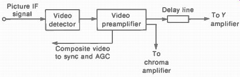
FIGURE 17-2 FUNCTIONS OF THE VIDEO PREAMPLIFIER STAGE
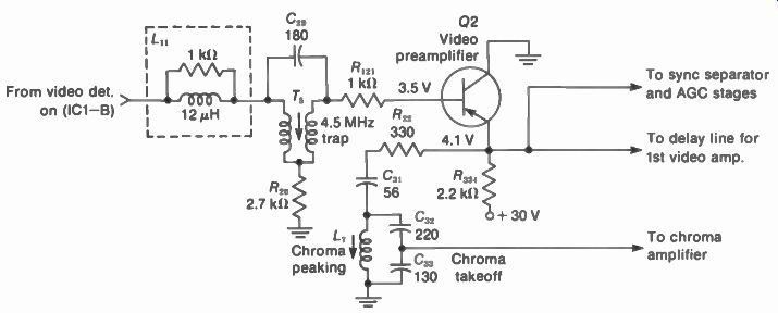
FIGURE 17-3 TRANSISTOR VIDEO PREAMPLIFIER CIRCUIT R IN OHMS AND C IN PICOFARADS.
(FROM RCA CHASSIS CTC-59)
Output signals from Q2 are taken from the top of R 321 for sync, AGC, and the delay line. The third output is from the chroma takeoff circuit to the input of the chroma amplifier, which is on an IC unit. The chroma peaking coil L7, together with C32 and C33, forms a low-Q circuit resonant at 4.1 MHz. This circuit compensates for the tilt of the chroma side bands in the response curve of the picture IF amplifier.
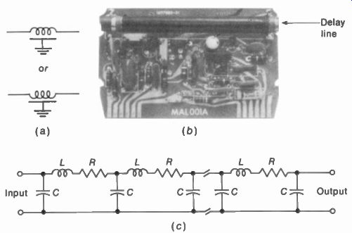
FIGURE 17-4 DELAY LINE FOR Y SIGNAL. (a) SYMBOL; (b) MOUNTING ON PLUG-IN
MODULE; (c) EQUIVALENT CIRCUIT.
Delay line. The narrower bandwidth of 1 MHz for the chroma circuits delays the signal more than the 3.2-MHz bandwidth of the Y amplifiers.
Without a time delay for the Y signal, it will arrive at the CRT ahead of the color image and the two will not be exactly superimposed. All that is required to prevent this problem is approximately 0.8 As delay in the Y signal. This is accomplished by installing an LC delay line, usually in the output of the video preamplifier.
The delay line is usually a coil about 8 in. long (Fig. 17-4). It consists of an insulating tube covered with a foil strip over which is a tightly wound coil. The entire unit is covered with an insulating coating. Terminals are brought out from the coil and the foil strip, which is grounded.
A delay line is similar to a transmission line in that it must be terminated with a resistance equal to its characteristic impedance (Zo). A typical value of Zo for the delay line is 680 Ohm.
17-3 The Y-Channel Video Amplifier
The composite video must be amplified enough to provide about 120 V p-p of Y signal to drive the picture tube. An example of a hybrid Y channel is shown in Fig. 17-5. It includes a PNP transistor for the Q304 preamplifier or first video amplifier and a vacuum tube V301 for the second amplifier, which is the video output stage. The delay line for Y signal is between the first and second amplifiers. The Y amplifier has the contrast control to vary the amount of luminance signal.
It is important to note that the video signal in the plate circuit of the output tube is dc coupled to the cathodes of the color picture tube. The direct coupling means that dc voltages on the output tube affect the cathode-grid bias on the CRT. This is why the brightness control for biasing the picture tube can be in the grid circuit of the video output stage. An advantage of this method for color picture tubes is that one brightness control in the video amplifier controls the bias for all three guns.
In addition, vertical blanking pulses are applied in the grid circuit of the video output stage. This way the pulses are amplified before being coupled to the CRT cathodes, to blank out the vertical retrace lines. The polarity of the blanking pulses is negative at the grid of the output tube. This is inverted to positive-going pulses in the output for the picture tube. Positive polarity is needed at the cathode to cut off the beam current for blanking.
For the video preamplifier in Fig. 17-5, composite video from the detector is coupled to the base of Q304. This signal has positive sync polarity. The amplified output is available at the emitter and collector. The 330-0 R321 is the emitter load resistor. There is no phase inversion here. This path acts as an emitter-follower to supply signal for the AGC circuit and for the chroma bandpass amplifier.
In the collector circuit, the 3.3-k-O R325 is the load resistor. This amplified signal has inverted polarity, with negative sync phase. From the collector, the Y signal goes through 3.58-MHz traps, which keep the chroma signal out of the Y channel, and the delay line DL101.
The diode D302, coupling capacitor C333 and peaking coil L, with damping resistor R334 complete the signal path to the grid of the video output tube. Also coupled to this grid are the vertical blanking pulses, which are isolated by D302. The negative pulses cannot flow from anode to cathode. However, the diode is turned on by positive voltage at the anode to conduct the video signal from cathode to anode.
In the output circuit of V301, the 5.6-k-O R338 is the plate load. T 302 provides high frequency peaking. The drive controls R341and R342 are adjusted to balance the Y video signals for the blue and green guns to the full output for the red gun. All video signal is removed by the service switch S102 to provide a blank raster for purity adjustments.
Fig. 17-5
In the cathode circuit of V301, the 350-ohm R143 varies the cathode bias to adjust gain for the Y signal and contrast in the picture. The peaking or sharpness switch S1 „, adjusts the bypassing in the cathode circuit. This controls the high frequency response by varying the amount of degeneration. The top portion of S 1 „, provides maximum sharpness, with minimum degeneration of the high video frequencies for maximum peaking.
The brightness control R13, is in the grid circuit of the video output tube, instead of the CRT circuit, because of the dc coupling. Positive voltage on R139 comes from the 25-V source through the brightness limiter adjustment. Negative voltage is obtained from the grid-leak bias on the horizontal output tube. To decrease the brightness, the grid bias on V301 is made more negative. Then its plate current decreases and the plate voltage increases. This increase in positive voltage at the cathodes increases the bias of all three guns to decrease the beam current in the CRT for less brightness. The brightness limiter R330 is a setup adjustment on the chassis which prevents blooming at the highest level of brightness for R139.
FIGURE 17-6 CHROMA BANDPASS AMPLIFIER USING PENTODE TUBE. R IN OHMS AND C IN PICOFARADS. (a) CIRCUIT: (b) OVERALL CHROMA RESPONSE FROM MIXER GRID TO CHROMA OUTPUT.
17-4 Chroma Bandpass Amplifiers
This section uses one or two stages tuned to 3.58 MHz to amplify the modulated chroma signal. The input is colorplexed video signal from the video preamplifier, as shown in Fig 17-6.
The amplified output is 3.58-MHz chroma signal to the color demodulators. The chroma section is considered a bandpass amplifier because its total bandwidth of 1 MHz is a relatively large percentage of the resonant frequency of 3.58 MHz.
Specifically, the bandwidth ratio is 1/3.58 = 0.28 or 28 percent.
This stage is generally called the bandpass amplifier (BPA), the color IF amplifier, the chroma amplifier, or simply the color amplifier.
Requirements of the chroma amplifier. Whether the amplifier has one or two stages, or uses tubes, transistors, or an integrated circuit (IC), the following features are necessary:
1. The amplifier must be tuned to 3.58 MHz with the required bandwidth. In Fig. 17-6a, the peaker coil L, and transformer T, are tuned to provide the desired chroma response. T, is resonant at 3.58 MHz, but L, peaks at higher frequencies to compensate for the sloping response for the chrominance signal in the picture IF amplifier. The overall response of the picture IF amplifier and chroma amplifier is shown by the curve in Fig. 17-6b.
2. The chroma signal level is varied to control the color saturation in the picture. In Fig. 17-6a, the potentiometer R2 is the color control that varies the amount of chroma signal to the demodulators.
3. Automatic chroma or color control (ACC) is used to determine the bias on the amplifier, in accordance with signal strength. As a result, the color level in the picture remains constant when stations are changed. In Fig. 17-6a, the grid bias for the pentode tube is controlled by the ACC circuit. The burst amplitude determines the ACC bias.
4. When no color signal is received, the chroma amplifier is cut off by a bias voltage applied from the color killer (CK) circuit. In Fig. 17-6a, the chroma amplifier is cut off by negative bias of about -30 V at the control grid. The chroma circuits must be killed because high-frequency components of the monochrome signal can be demodulated to produce color at vertical edges in a black and-white picture.
5. The chroma amplifier is keyed off during horizontal retrace time, in order to remove the burst from the chrominance signal to the demodulators. In Fig. 17-6a, positive flyback pulses are applied to the cathode to cut off plate current. The burst is removed here because different levels of burst for different stations can change the dc clamping level for the detected color video. This affects the color temperature adjustments for the picture tube.
Pentode chroma amplifier. In Fig. 17-6a, the single pentode tube is the complete chroma amplifier. Cathode bias is provided by R, and Ck, in addition to the grid bias from the ACC circuit.
Typical bias is -2 V, operating as a class A amplifier for the 3.58-MHz chroma signal input from the video preamplifier. The amplified output is 6 V p-p, which can be varied by the color control.
The tuning adjustments are L, in the grid input and T, in the plate output circuit. R f and C f form a decoupling filter for the 280-V supply to the plate. C: , tunes T, to 3.58 MHz. R, is a damping resistor to provide the required bandwidth. A typical 3.58-MHz bandpass transformer is shown in Fig. 17-7.
FIGURE 17-7 A 3.58-MHz BANDPASS TRANSFORMER HEIGHT IS 172 IN
FIGURE 17-8 CHROMA AMPLIFIER USING IC UNIT R IN OHMS AND C IN PICOFARADS
(FROM SEARS MODEL 4360)
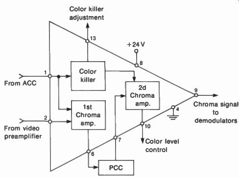
FIGURE 17-9 BLOCK DIAGRAM OF THE /C301 UNIT FOR THE CHROMA AMPLIFIER IN FIG.
17-8.
IC chroma amplifier. The integrated circuit in Fig. 17-8 includes two chroma amplifier stages and the color killer, as shown in the block diagram in Fig. 17-9. Referring to Fig. 17-8, colorplexed composite video signal is applied to pin 2 of IC301, through the 4.5-MHz traps.
Amplified chroma signal at 3.58 MHz is available at pin 6. The gain is controlled by ACC bias developed in another IC unit, not shown.
Before the chroma signal from tie first amplifier out at pin 6 is coupled to the second amplifier in at pin 7, a peak chroma control (PCC) stage is used. Its function is to prevent excessive color saturation by clipping the signal peaks if the chroma amplitude exceeds a specified level. The output from the second chroma amplifier is out at pin 9 to the chroma demodulators. A 24-V source is applied to pin 8 to supply dc power for all stages, with respect to ground at pin 4.
Note the one-button control (OBC) switch at pin 10 of IC301. With this switch in the off position, the manual color level control R, adjusts the gain for the chroma level. When OBC is turned on, however, the 47-k-o resistance of R: , is added in series. Then the manual control has little effect and the color level is determined by the preset OBC adjustment R. The color killer connection at pin 13 provides a dc voltage to cut off the second chroma amplifier on a monochrome program.
Chrome alignment. The response curves in Fig. 17-10 apply. The picture IF response out of the video detector is shown in Fig. 17-10a. The color subcarrier at 42.17 MHz is at 50 percent response on the slope opposite the side for the picture IF carrier. This method is used because it would be too difficult to have the 42.17 MHz at full gain and keep the sound signal at 41.25 MHz from interfering with the color signal. Figure 17-10b shows the compensating response of the chroma amplifier itself. This curve peaks a little above 4.1 MHz. The opposite slopes of Fig. 17-10a and b result in the overall response in c for the 3.58-MHz chroma signal. This curve is at the input to the chroma demodulators, including the gain of the picture IF amplifier and chroma amplifier.
If you were to align only the chroma bandpass amplifier, with its peaker circuit, you would look for the sloping response in Fig. 17-10b. This method is rarely used, however, because it is difficult to get the response exactly right. Usually, the chroma bandpass is part of the overall picture IF alignment.
17-5 The Burst Amplifier Stage
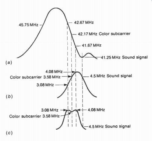
FIGURE 17-10 ALIGNMENT CURVES FOR CHROMA SIGNAL. (a) SLOPING RESPONSE IN
PICTURE IF AMPLIFIER: (b) OPPOSITE SLOPE IN CHROMA AMPLIFIER: (c) COMBINED
RESULT WITH 4.5-MHz TRAP.
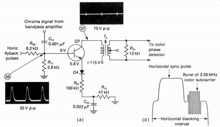
FIGURE 17-11 (a) BURST AMPLIFIER CIRCUIT TO SEPARATE 3.58-MHz BURST SIGNAL
SHOWN IN (b)
The reference phase for regenerating the sub carrier in the color oscillator is transmitted as a burst of 8 to 11 cycles of 3.579545-MHz signal on the back porch of each horizontal blanking pulse. (See Fig. 17-11.) Since the burst occurs during horizontal blanking time, it is easily separated from the chroma signal. The burst amplifier is simply a stage that is normally off but is keyed on during horizontal retrace. Two methods of keying on the burst separator are:
1. Flyback pulses from the horizontal output circuit.
2. Horizontal sync pulses from the sync separator. The sync pulses must be delayed approximately 4 is so that they occur during the back porch of horizontal blanking when the burst is present.
The method of delayed sync has the ad vantage of making the burst separation independent of the flyback pulses. Their timing can vary with the horizontal hold control and with the way the AFC circuit locks in the horizontal oscillator.
This stage is generally called the burst amplifier, burst separator, or burst gate. The signal that has the burst can be taken from either the video preamplifier or a chroma stage before blanking. A typical 3.58-MHz transformer for the burst amplifier is shown in Fig. 17-12.
For the transistor Q7 in Fig. 17-11, note that the dc voltages normally hold the stage cut off. There is no forward bias at the base. The 5.6 V at the N emitter of the NPN transistor is a reverse bias. However, the 35-V positive flyback pulses applied to the P base are able to key the transistor on during the time the burst signal is present. Therefore, only the burst is amplified to appear in the collector output with an amplitude of 75 V. The burst transformer T. couples the burst signal to the color phase detector used for AFPC on the color oscillator.
When there is no AFPC circuit, the amplified burst can ring the oscillator crystal directly to lock it in the correct phase.
FIGURE 17-12 A 3.58-MHz TRANSFORMER FOR BURST AMPLIFIER. HEIGHT IS 1/ 2 IN.
The amplifier in Fig. 17-11 is basically a common-emitter stage, with input signal to the base and the output signal transformer-coupled from the collector. In the base circuit, R,4 „ isolates the burst amplifier from the horizontal output circuit. In the emitter circuit, the split resistance of R„, and R4, has several functions.
First, the resistors help to limit the base current to a safe value. Note that D4 has the polarity to block reverse current, but that it conducts for forward electron flow into the emitter. In addition, R„, and R41 provide dc bias and stabilization in the emitter circuit. Finally, the 100-k-O R„, is not bypassed in order to provide ac feedback for degeneration of the input signal. The purpose is to prevent the high-amplitude flyback pulses in the input from appearing in the output circuit.
17-6 Color Oscillator and Synchronization
The color oscillator regenerates the 3.58-MHz color subcarrier needed in the receiver for the demodulators. This function is necessary be cause the subcarrier is suppressed in transmission of the color signal.
The input to the color oscillator is the synchronizing voltage needed to hold the hues steady. Although the oscillator uses a 3.579545-MHz crystal for frequency stability, it must be locked into the phase of the burst signal. Either the burst voltage is injected directly into the oscillator circuit or an AFPC circuit compares the oscillator and burst phase to produce a dc control voltage for the oscillator.
The manual hue or tint control is a phase adjustment in the oscillator or its control circuit.
The oscillator output is a 3.58-MHz continuous wave, or ow, signal. This means it has no modulation.
The oscillator synchronizing circuits have the additional functions of turning the color killer off for a color program and providing ACC bias for the chroma bandpass amplifier. The color killer depends on the presence or absence of burst signal. The ACC bias depends on the burst amplitude. The amount of burst can be determined by a control voltage from either the burst phase detector or the bias on the oscillator. These features can be seen in the block diagrams of Fig. 17-13, illustrating different types of circuits for the color oscillator and its synchronization.
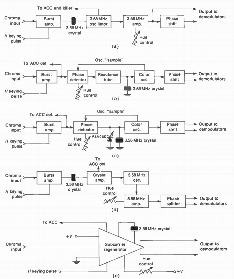
FIGURE 17-13 TYPES OF CIRCUITS FOR 3.58-MHz COLOR OSCILLATOR AND ITS SYNCHRONIZATION.
(a) RINGING OSCILLATOR LOCKED IN DIRECTLY BY BURST SIGNALS; (b) FREE-RUNNING
OSCILLATOR CONTROLLED BY REACTANCE TUBE; (c) OSCILLATOR CONTROLLED BY VARICAP
INSTEAD OF REACTANCE TUBE; (d) COMBINATION OF RINGING AND FREE-RUNNING OSCILLATOR;
(e) IC UNIT.
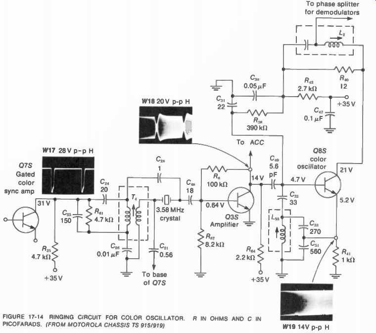
FIGURE 17-14 RINGING CIRCUIT FOR COLOR OSCILLATOR. PICOFARADS (FROM MOTOROLA
CHASSIS TS 915/919) R IN OHMS AND C IN
For the ringing circuit in Fig. 17-13a, the burst signal shocks the crystal into oscillation at exactly the same frequency and phase as the color sync. Because the crystal has very high Q, its oscillations continue through the time from one pulse of burst to the next. The amplitude of oscillations depends on the amplitude of burst signal. Actually, the stage labeled as the oscillator is an amplifier for the crystal oscillations.
The next amplifier stage is also a limiter to provide constant output of oscillator ow signal for the demodulators.
The circuit in Fig. 17-13b uses a free-running crystal oscillator, but the phase and frequency are controlled by the reactance tube.
Its reactance is varied by a dc control voltage from the phase detector. Two diodes are used in a discriminator circuit that compares the color burst signal to a sample of the color oscillator output. Essentially the same circuit is shown in F g. 17-13c, but a semiconductor capacitive diode, varactor, or varicap, is used instead of the reactance tube.
Figure 17-13d shows a combination of ringing with a free-running oscillator. The burst pulses excite the crystal, and the amplified output synchronizes a Hartley or Colpitts type of oscillator.
The last example, Fig. 17-13e, uses a single IC unit, which is the subcarrier regenerator. It contains all the semiconductor components necessary to generate and synchronize the color oscillator. The connections required include the dc voltage source, labeled V, chroma signal input with the burst, horizontal keying pulses, and an external 3.579545-MHz crystal.
The output includes the necessary oscillator cw signal for the color demodulators, plus a dc volt- age proportional to the burst signal that can be used for ACC bias and the color killer.
Ringing circuit for color oscillator. This method can be used with tubes or transistors, but a transistorized circuit is shown in Fig. 17-14. The separated burst signal from Q7S shock-excites the 3.58-MHz crystal. This output is amplified by Q3S to drive Q8S which is a Colpitts oscillator circuit.
The burst transformer for the first stage is T,. Note that C2„ is used to provide some re generative feedback to help maintain crystal oscillations between burst pulses. The crystal output amplifier Q3S serves as a buffer stage to isolate the crystal from loading by the oscillator stage.
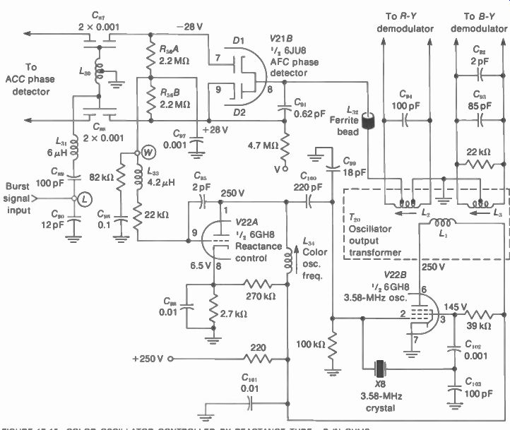
FIGURE 17-15 COLOR OSCILLATOR CONTROLLED BY REACTANCE AND C IN MICROFARADS
(FROM ZENITH CHASSIS 25LC30) TUBE R IN OHMS
Except for the crystal input signal, the color oscillator Q8S is a typical modified Colpitts circuit. Feedback is from the emitter into the oscillator tank circuit at the junction of C3:, and C, across the oscillator coil L„. Wave form W19 at the emitter shows how the amplitude of the oscillator signal is now constant compared with W18. The output is taken from the collector through 1_ 2 to a phase splitter stage, which supplies oscillator cw to the color demodulators.
The most important change in the wave form cannot be identified in the photos. That is the phase of the oscillator, which is synchronized exactly to the crystal input signal. This synchronization occurs by brute force as the amplitude of the crystal input signal is larger than the free-running amplitude of the oscillator.
Color oscillator with reactance tube. See Fig. 17-15. The dual diode V2113 is a phase detector for color AFC. It detects the phase difference between color burst and a sample of the oscillator output. The output is a dc control voltage for bias on the reactance tube* V22A. This stage holds the color oscillator frequency locked in with a specific phase compared with the burst signal.
The color phase detector operates in practically the same way as a sync discriminator for horizontal AFC. However, the color AFC circuit compares the burst signal with a sample of the oscillator output 90 deg out of phase with burst.
When the color oscillator signal is correct, the output of the phase detector is zero. Then both diodes conduct the same amount.
If the phase of the oscillator drifts, its signal will not be exactly in quadrature with the burst signal. Then one diode conducts more than the other and the detector output will go either positive or negative. The polarity indicates whether the oscillator output changed above or below 90°. The dc control voltage is coupled to the control grid of the reactance tube. The change in bias controls the reactance to correct the oscillator. Phasor diagrams of the signals into the color AFC phase detector are shown in Fig. 17-16.
The color oscillator V22B is a Pierce circuit, with the screen grid as the oscillator anode.
This makes the stage an electron-coupled oscillator, isolating the oscillator circuit from the output load in the plate circuit. The windings on the oscillator output transformer supply cw input to the R - Y and B - Y demodulators. The 22-k-o resistance across L : , allows this phase to be opposite burst phase for the B - Y signal.
The 100-pF capacitance across L, makes this circuit resonant to provide quadrature phase for the R - Y signal.
[[*Operation of the reactance tube is the same as described for an FM signal in Section 27. ]]
The hue control is not shown in Fig. 17-15 because it is in the output of the burst amplifier.
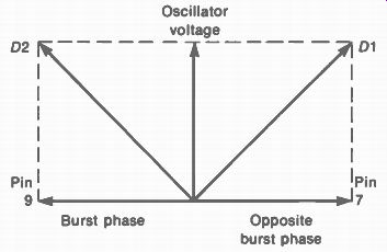
FIGURE 17-16 PHASOR DIAGRAM FOR THE OSCLLATOR AND BURST VOLTAGES APPLIED
TO THE AFC PHASE DETECTOR IN FIG. 17-15.
Burst phase
Variation in hue is accomplished by slightly shifting the phase of the burst signal out of the amplifier and into the phase detector. This phase change causes a shift in dc control voltage. The change in bias on the reactance tube shifts the phase of the oscillator output. Finally, the phase shift is in the R - Y and B - Y cw signals to the demodulators, resulting in different hues in the detector output.
17-7 AFPC Alignment
Either misalignment or trouble in the automatic frequency and phase control circuit shows as a loss of color sync in the picture. The result is color bars, as shown in color plate VI. Other symptoms are wrong hues in the picture or a narrow range with the tint control. If the color locks in well for a strong signal but not for weaker stations, this may be caused by poor AFPC action. Normally, if there is color to see in the picture, it should lock in.
You can estimate the frequency error in the 3.58-MHz oscillator by counting the number of color bars. Each pair of horizontal bars corresponds to 60 Hz off the correct frequency. In color plate VI, the five pairs of color bars show that the color oscillator is 5 x 60 = 300 Hz off the frequency of 3.58 MHz. As the oscillator frequency comes closer to 3.58 MHz, there are fewer bars. For errors of less than 60 Hz, you can see diagonal colors. When the oscillator frequency is at 3.58 MHz but not locked in sync, the colors change from a solid picture to drifting bars. This condition is called zero beat for adjusting the color oscillator, meaning that it is on frequency although not locked in.
In addition to the fact that the colors must be locked in, the tint control should vary the hues from purple at one end to green at the opposite end, with correct flesh tones in the center.
The range of the tint control is determined by the AFPC adjustments.
The following general procedures for AFPC adjustments apply to most receivers:
1. Use a color bar generator to see all the hues in the picture. With sync, the vertical color bars are locked in. However, without color sync you see diagonal colors across the vertical bars.
2. Set the manual hue or tint control to the center of its range.
3. Disable the color killer. This turns on the chroma bandpass amplifier. Have the color control at maximum.
4. Turn automatic color circuits off.
5. Tune the 3.58-MHz burst circuits for maximum output.
6. Tune the 3.58-MHz color oscillator for maximum output at the correct frequency.
Without any burst input, the oscillator is on frequency at the point of zero beat, when the color bars drift very slowly.
After the AFPC adjustments, make sure all controls are back to normal and the color is locked in. If necessary, the color oscillator can be readjusted slightly to give the tint control the desired range. Set the color killer to remove color snow on an unused channel.
17-8 Chroma Demodulators
The chroma signal from the bandpass amplifier consists of the side bands produced by modulation of the 3.58-MHz color subcarrier. However, the color subcarrier itself is suppressed in trans mission. This 3.58-MHz cw signal is reinserted in the demodulators by the output of the color oscillator. Then the chroma side bands can beat with the 3.58-MHz subcarrier so that the color video signal can be detected as the difference frequencies between the side bands and the subcarrier. An important factor in this method is that the detected output depends on the phase of the reinstated subcarrier. This is why the color demodulator is called a synchronous detector.
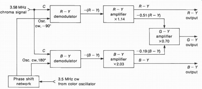
FIGURE 17-17 BLOCK DIAGRAM OF R V. BY DEMODULATION SYSTEM WITH COLOR DIFFERENCE
AMPLIFIERS
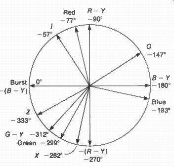
FIGURE 17-18 HUE PHASE ANGLES FOR COLOR DEMODULATORS. VALUES ARE SHOWN NEGATIVE
IN THE CLOCK-WISE DIRECTION FROM BURST AS THE REFERENCE.
The basic arrangement for the color de modulator circuits is illustrated by the block diagram in Fig. 17-17. Tubes or transistors can be used, including diodes and integrated circuits. With two demodulators, two color-difference signals are detected. These are usually R - Y and B - Y video, which are combined to form G - Y. Then the color-difference signals are matrixed to form R, G, and B video signals.
The end result required is red, green, and blue video for the picture tube. Some circuits use R, G, and B demodulators to detect the red, green, and blue video directly. The hue of the detected output signal from the color demodulator depends on the phase of its oscillator cw input.
Any hue has its own phase angle.
Note the multiplying factors shown for the amplifiers in Fig. 17-17. These are correction values to compensate for the relative amplitudes used in the modulation at the transmitter.
The relative gain for the R - Y video amplifier is 1.14 because the signal is reduced by the factor of 'I 14 t0 prevent overmodulation. Similarly, the relative gain for the B - Y amplifier is 2.03. In brief, the B - Y detector output is boosted by almost double the gain of the R – Y signal. However, the G – Y gain is reduced by the factor of 0.70 or 71.14 because this signal is increased by the factor 1.4 in modulation. This amplitude correction is applied before the R - Y and B - Y signals are combined to form G - Y. For the corrected signals, G - Y is equal to 51 percent of (R Y) and 19 percent of (B Y). Phase angles for the demodulators. The combination of R - Y and B - Y demodulators is most common because these two axes are in quadrature. B - Y phase is 180-deg from burst phase. The hue for R - Y is at 90', exactly between the phase of burst and B - Y. The quadrature phase is preferred because a synchronous detector produces maximum signal output for the phase of its cw input but minimum for any signal 90" out of phase. Signal that is 180-out-of-phase also produces maxim um output, but of opposite polarity.
For R, B, and G demodulators, three detectors are needed. These have oscillator cw input at -77', -193", and - 299°, as shown in Fig. 17-18. Note that these angles are with respect to burst as the reference at 0'. The negative sign indicates the clockwise direction.
Another combination uses X and Z demodulators. The X axis is at -282°, close to the phase of -(R - Y).
The Z axis is at 333°, close to -(B - r or burst phase. Actually, the X and Z demodulators just form a balanced circuit, with a G- Y adder to provide R- Y, B- Y, and G - Y video signals in the output. This result is determined by the relative amplitudes for the detector output voltages.
The /and Q modulation axes for the transmitted chroma signal are practically never used at the receiver because of the extra bandwidth of the I signal. The receiver circuits are much simpler when the detected color video signals all have the same bandwidth of 0.5 MHz.
Basic demodulator requirements. Figure 17-19 shows the circuit of a B - Y demodulator using a pentode tube. The same circuit can be used for R - Y, X, or Z demodulators, the only difference being the phase of the oscillator cw input. Also, the circuit can use a triode tube, transistor, or diode. It is only required to have two inputs, the 3.58-MHz chroma signal from the bandpass amplifier and the 3.58-MHz cw subcarrier from the color oscillator.
For the pentode in Fig. 17-19, the oscillator cw is applied to grid 1. This signal at the control grid can be considered as keying on or off the conduction of plate current (/ _p) for the chroma signal applied to grid 2. Note that the B - Y phase of the oscillator cw is close to the phase of blue in the chroma signal but opposite from yellow. Maximum I _p flows for blue, then, as both signals have the same phase. Minimum 1 _p flows for yellow. Therefore, the demodulator has its maximum peak-to-peak value for hues on the axis of blue and yellow. Chroma signal of the quadrature phase has little effect on the output.
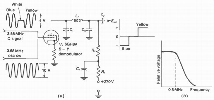
FIGURE 17-19 (a) CIRCUIT WITH PENTODE TUBE FOR B Y DEMODULATOR, (b) VIDEO-
FREQUENCY RESPONSE FOR DETECTED OUTPUT.
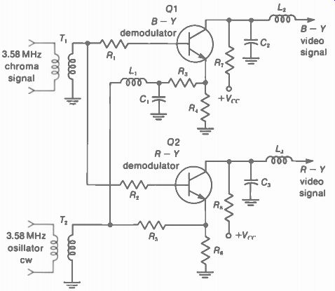
FIGURE 17-20 TRANSISTOR CIRCUITS FOR B 1' AND R - Y DEMODULATORS.
In the demodulator output circuit, the variations in / _p produce video signal voltage across R _p. The polarity of the output is inverted from the input as the plate voltage decreases because of a larger voltage drop across R1 with more / _p. The video peaking coil L,. with the shunt capacitance of C, and C, provides the video frequency response up to 0.5 MHz shown in Fig. 17-19b. In brief, the color information is in the 3.58-MHz chroma signal before the demodulators, but after detection the color video signals have the bandwidth of 0 to 0.5 MHz.
Transistors for the demodulator circuits. See Fig. 17-20, with NPN transistors Q1 and Q2 used as 8 - Y and R - Y demodulators. For each stage, chroma signal is coupled to the base by T. Also, oscillator cw signal is applied to both emitters by T1. Note that there is no forward bias voltage at either base. Therefore, the ac input signals drive the transistor into conduction. Effectively, the base-emitter serves as a diode rectifier for synchronous demodulation, and the detected resultant is amplified in the collector output circuit. For Q1, R7 is the load resistance and I-2 the peaking coil for the B - Y color video signal. Similarly, Rs is the collector load and the peaking coil for R - Y signal from Q2. Then the R - Y and 8 - Y signals can be combined in a G - Y adder, not shown here.
IC demodulator module. See Fig. 17-2. The integrated circuit here is one of two small modules with IC units that contain all the chroma stages. The other IC, not shown, has the bandpass amplifier, color killer, burst amplifier, color oscillator, and AFPC circuits. In Fig. 17-21, this IC unit has R - Y and B - Y demodulators, the G - Y adder, and three emitter-follower stages to isolate the output signals. Each goes to a separate module for matrixing and video drive to the red, blue, and green guns of the picture tube.
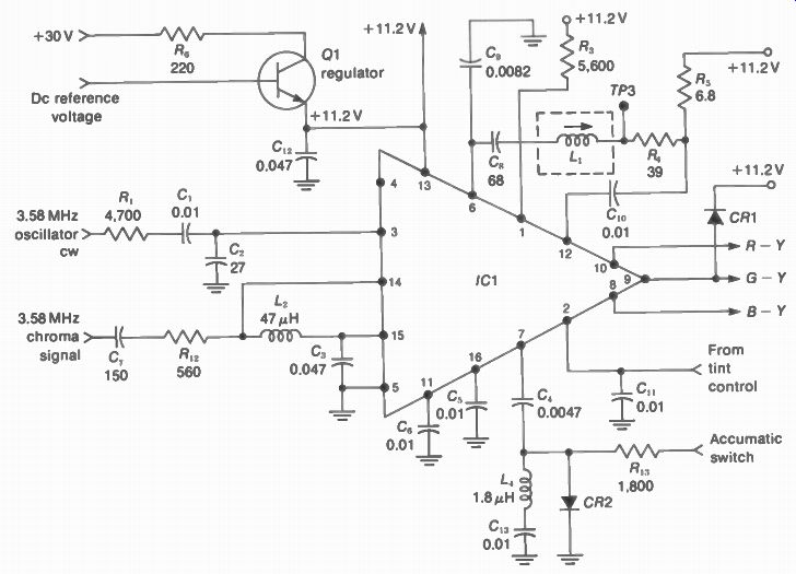
FIGURE 17-21 IC DEMODULATOR R IN OHMS; C MORE THAN 1 IN PICOFARADS (pF),
LESS THAN 1 IN MICROFARADS (SF). (FROM RCA CHASSIS CTC 59)
The 3.58-MHz chroma signal for demodulation is applied to pin 14 of /C1 in Fig. 17-21. This is applied directly to the R - Y and B - Y demodulators. The oscillator cw signal input at pin 3 is amplified and limited for constant amplitude before being applied to the demodulators with the required quadrature phases. The only external adjustment is the tuning coil L _p which is set for maximum 3.58-MHz oscillator cw at test point TP3. This circuit provides the 90° phase shift for the R - Y demodulator.
Control of the tint or hue is accomplished at pins 2 and 7. A dc voltage from the tint control on the front panel is applied to pin 2. This voltage controls the phase of the oscillator cw signal amplified within the IC unit. At pin 7, the voltage depends on the Accumatic switch, which is the RCA name for one-button color.
Normally, the signal at pin 7 is grounded through C, and CR2. The diode is biased into conduction by 11.2 V at its anode with the Accumatic switch off. When the switch is on, this positive voltage is removed and the diode is turned off. Now pin 7 goes to ground through C _p L _p and C1 „. This network establishes a fixed phase angle for the oscillator cw signal for proper flesh tones, even if the manual tint control is set wrong.
The regulator stage Q1 in Fig. 17-21 supplies 11.2 V regulated dc collector voltage for the stages in IC1 and other modules. At the base of the regulator the reference is 11.2 V from a zener diode. C is a bypass capacitor for the 11.2-V supply line from the emitter of Q1.
Similarly C„, C5, and C„ are bypass capacitors for the internal stages of the IC unit.
Diode demodulators. In Fig. 17-22 two dual diode units D1 and D2 are used for B - Y and R - Y demodulators. In each unit, the diodes are series-aiding, with the anode connected internally to the cathode. Externally, the three terminals include a cathode at 1, the opposite anode at 2, and the common center connection at 3. The oscillator cw signal is applied push pull to terminals 1 anki 2 by the input transformer T,. This is connected to both the R - Y and B - Y demodulators without any 90-deg phase shift.
Instead, the chroma signal from input transformer L is shifted 90° for the R - Y demodulator D2. The quadrature phase is provided by L, with C,„ and C,6. The chroma signal is applied to the center terminal 3 of the demodulators.
In this circuit, the chroma signal has the quadrature phase for the R - Y demodulator, instead of using 90° for the oscillator cw signal.
However, the results are the same. The advantage is that the push-pull oscillator cw signal can be balanced for zero output when the chroma signal input is zero.
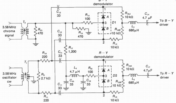
FIGURE 17-22 DIODE DEMODULATOR CIRCUITS R IN OHMS AND C IN PICOFARADS. (FROM
MAGNAVOX CHASSIS 7979)
Each diode pair detects its phase of chroma signal to produce color video output.
This signal is taken from the center connection of either R,2 or R,„ as a center-tapped diode load resistor. The voltage at this point corresponds to the voltage at terminal 3 between the diodes A and B in the demodulator. When the oscillator cw signal is in phase with the chroma signal, one diode conducts more than the other. For opposite phases, the opposite diode conducts more. The result is maximum output signal for B - Y phase from D1 and for R - Y from D2.
In either demodulator, there is no crosstalk between quadrature signals. Then both diodes conduct the same, which results in zero output because of the balance.
Summary of demodulator action. For any type of synchronous demodulator, two input signals are required: a 3.58-MHz modulated chroma signal and a 3.58-MHz oscillator cw signal. The result is synchronous detection in the following steps:
1. When the oscillator cw and chroma input have the same phase, the output amplitude increases.
2. When the oscillator cw and chroma input have opposite phases, the output amplitude decreases below the medium level.
3. When the oscillator cw and chroma input are 90 deg out of phase, the output amplitude corresponds to zero oscillator cw signal. The reason is that for 90° phase, one signal is at zero when the other is maximum.
4. With varying amplitudes of chroma signal, the amount of detector output varies in pro portion to the amplitude.
5. With varying phases of chroma signal, the detector output varies in proportion to the phase change.
6. As a result, the demodulator detects only the phase of chroma signal corresponding to the phase of the oscillator cw input.
It is important to note that the color demodulator is where the color video signals are extracted from the 3.58-MHz chroma signal. For the input there is just one chroma signal. Its frequency is 3.58 MHz with a bandwidth of ± -0.5 MHz. In the detected output, there are separate video signals for red, green, or blue with a bandwidth of 0 to 0.5 MHz.
17-9 Matrixing the Y Video and Color Video Signals
Matrixing means combining or adding signals.
An example is adding R - Y and B - Y to form G - Y. The most important application in the receiver, though, is matrixing the color-difference signals with Y video to form the red, green, and blue video signals needed for the three guns of the picture tube. This matrixing for R, G, and B can be done either in the picture tube or in the color video circuits. Examples are shown in Figs. 17-23 to 17-25.
Matrixing in the picture tube. This method in Fig. 17-23 is commonly used with vacuum tube amplifiers. The control grid of each gun in the picture tube has R - Y, B - Y, or G - Y video signal. All three cathodes have the same -V video signal. The polarity is negative for Y signal at the cathode because the effect of cathode voltage on beam current is opposite that of grid voltage. Effectively, then, each grid has R, G, or B video signal to control beam current for the color information, as the Y component in the color signal at the grid is canceled by the Y signal at the cathode. Algebraically, the matrixing for the color video signals can be added as follows:
(R - Y) - (-Y) = R - Y+ Y= red video
(G - Y)- (-Y) = G- Y+ Y= green video
(B - Y) - (-Y) = B - Y+ Y= blue video
The same algebraic combinations can be used when the Y signal and color video signals are all applied to the cathodes for the picture tube, with the grids grounded. This method is often used with transistor amplifiers as protection against arcing at the control grid in the picture tube. The color-difference signals at the cathode then have negative polarity, like the - Y signal. For red, as an example, --(R - Y) + (- Y) -R at the cathode.
Matrixing in color video amplifiers. Figure 17-24 shows an example of matrixing Y signal in an R - Y amplifier. The NPN transistor Q1 is a color video amplifier for -(R - Y) signal at the base, but Y signal is also injected at the emitter.
In terms of the input color signal, it is amplified and inverted to produce R - Y signal at the collector. However, the Y signal at the emitter is amplified without phase inversion. The resultant output signal from the collector is equivalent to R Y + Y - R.
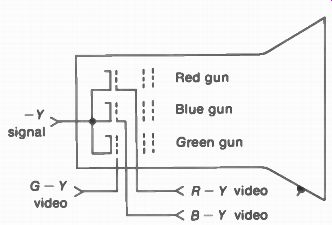
FIGURE 17-23 MATRIXING IN THE PICTURE TUBE
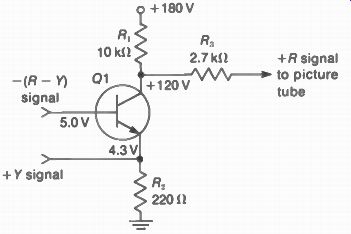
FIGURE 17-24 CIRCUIT FOR MATRIXING (R Y) AND Y SIGNALS IN A COLOR VIDEO AMPLIFIER
For the circuit in Fig. 17-24, the 10-kit R, is the collector load resistance. The 220-i2 R2 is the emitter resistance for Y input. For Y signal, the stage is effectively a common-base amplifier, without phase inversion. For the -(R - Y) signal at the base, the stage is a common-emitter amplifier. Both the Y and R - Y signals are developed in the collector output circuit. The 2.7-kit R, is an isolating resistance for the coupling circuit to the control grid of each gun in the picture tube.
Three stages such as Q1 would be used for the three color video signals. The output of each is positive R, G, or B video for the control grid in the picture tube. When the color video signals are applied to the cathodes in the picture tube, they have negative polarity, with -R, -G, and -B for cathode drive.
Matrixing in the demodulators. In Fig. 17-25, the Y signal is applied to the center tap of T, for the chroma input. As a result, the Y signal is in series with the chroma signal for D1 aid D2.
The two diodes form one demodulator circuit.
Three of these demodulators are used to detect R - Y, B - V. and G - Y. However, the matrixing of Y signal results in R, G, and B video output.
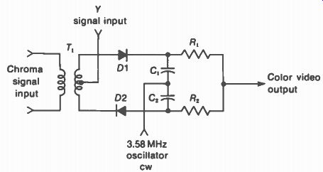
FIGURE 17-25 CIRCUIT FOR MATRIXING Y SIGNAL IN A COLOR DEMODULATOR. D1 AND
D2 FORM ONE DEMODULATOR CIRCUIT FOR DETECTING R V. B - V. OR G -- Y.
The Y signal will be passed through to the output whether or not a chroma signal is being received. If no signal is applied to the primary of T _p the Y signal will be the only signal applied to the anode of D1 and the cathode of D2 in the same phase. However, when chroma signal is present at T _p the Y signal will represent a changing voltage level at the secondary center tap. In this way, the chroma signal will be superimposed on the Y signal. Both signals will act on the two diodes. As a result, the Y signal will become part of the output.
The 3.58-MHz oscillator cw signal is connected to both diodes through C, and C. As the oscillator signal alternately turns the diodes on and off, the average current will depend on the polarity of the Y signal. When the Y signal is positive, D1 will conduct more than D2 and the output will be positive. When the Y signal is negative, D2 will conduct more than D1 and the output will be negative.
The 3.58-MHz chroma signal is smaller in amplitude than the Y signal. As a result, the demodulated color video will ride on the Y signal, much as an ac signal rides on a dc level when both are in the same circuit. This is desirable because the Y signal represents the bright ness component, while the chroma is the color.
The result, then, is that the correct brightness level is restored to the color video signal.
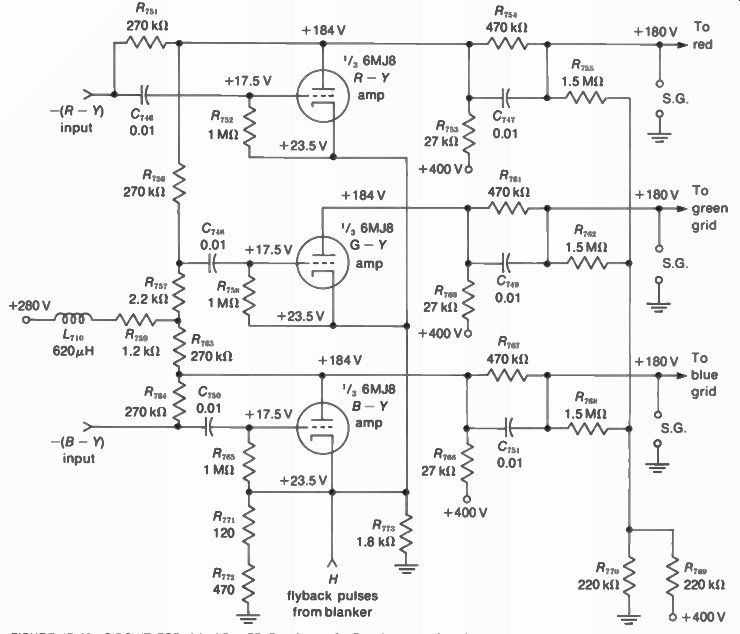
FIGURE 17-26 CIRCUIT FOR COLOR-DIFFERENCE AMPLIFIERS. R IN OHMS AND C IN
MICROFARADS. S.G. IS SPARK GAP FOR GRID OF PICTURE TUBE. (FROM ADMIRAL CHASSIS
2K20)
17-10 Video Amplifiers for Color
These circuits include color-difference stages such as the R - Y, B - Y, and G - Y amplifiers and the output stages for red, green, and blue video. When the Y video signal is matrixed in the picture tube, it is only necessary that the color video amplifiers have a bandwidth of 0.5 MHz for the color information. When Y signal is combined with the color signal, however, the video amplifier must have the bandwidth of 3.2 MHz to include the details of luminance. An advantage of matrixing the Y and color video signals in the color video circuits is the fact that the red, green, and blue video drive controls then proportion both the luminance and color video signals for the picture tube.
Color-difference amplifier stages. In Fig. 17-26, triple-triode 6MJ8 is used for all three color video amplifiers. The G - Y signal is obtained by combining signals from the R - Y and B - Y stages. One source is the common cathode resistor R771 , which is in parallel with the series combination of R 77 1 and R 772. This group is shown in the cathode circuit of the B - Y amplifier at the bottom of the diagram, but the combined resistance has the plate signal current of the three amplifiers. The other source for G - Y signal is from the plate circuits of the R - Y and B - Y amplifiers through the resistor network of /37 _p 7, and R76„ at the top left in the diagram.
The overall result is the proper amount of combined signal to form G - Y. Each triode is a video amplifier, with response up to 0.5 MHz for the R - Y, B - Y, or G - Y video signal.
The input signals are ac-coupled to the amplifiers by C71„, C7 , and C„„. In each stage, the coupling capacitor blocks any dc component of the signal level. However, the dc level is restored, effectively, by grid-leak bias. Then the amplified plate signal for each amplifier is directly coupled to its respective grid in the picture tube. The dc coupling means that the dc component reinserted in the grid circuit is applied from the plate circuit as part of the video signal drive for the picture tube. Grid-leak bias results from horizontal flyback pulses applied to the cathodes from a transistor blanker stage.
More details of the blanking will be shown in Fig. 17-29.
Output stage for blue video signal. The circuit in Fig. 17-27 amplifies the blue signal, with two more identical stages used for red and green video output. The Y signal has already been matrixed with the color video. As a result, the input here is one signal that has everything needed to drive one gun in the color picture tube, including the luminance and blue information. The amplitude of the video output signal is about 120 V p-p. Furthermore, the dc component has been reinserted in the signal by a previous stage, so that the video output stage is dc-coupled to the picture tube.
The input signal is applied to the base of Q8 as a CE amplifier. Base bias is provided by the dc level of the signal taken from an IC demodulator unit not shown here. The emitter voltage is made variable with R54 to control the gain. This is the blue drive control. Because of the dc coupling of the collector voltage, the drive control also varies the bias on the picture tube.
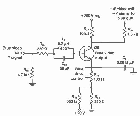
FIGURE 17-27 COLOR AMPLIFIER CIRCUIT FOR BLUE VIDEO DRIVE ( FROM MOTOROLA
CHASSIS TS938)
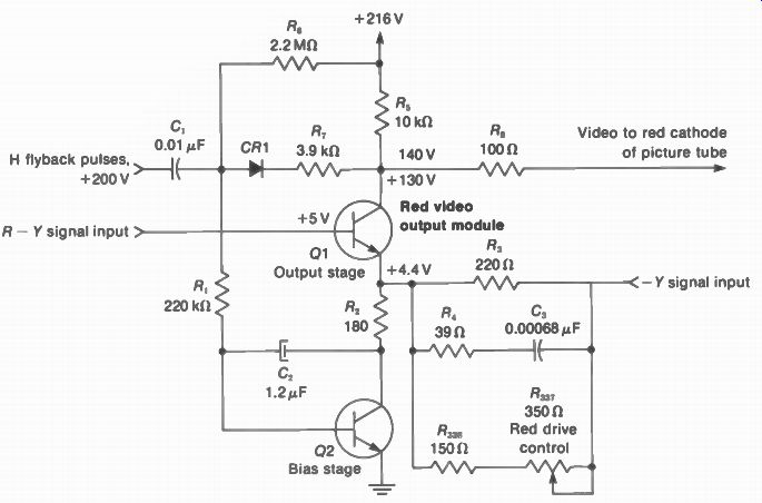
FIGURE 17-28 COLOR VIDEO AMPLIFIER THAT INCLUDES MATRIXING AND BLANKING.
(FROM RCA CHASSIS CTC 59)
Red video output module. In Fig. 17-28, Q1 is the video output transistor supplying all the signal needed for the red gun, including the red video, matrixed Y video, and blanking pulses.
Q2 is a bias transistor to control the current in the output stage. Both Q1 and D2 are on a small module board, with three separate modules (for red, green, and blue video output) to drive the picture tube.
17-11 The Blanker Stage
Figure 17-29 shows the same color-difference amplifiers as Fig. 17-26 but with the blanker Q710 added. This stage provides horizontal flyback pulses for the cathode of each amplifier.
Consider the R - Y amplifier at the top of the diagram. Since its output is coupled to the control grid of the red gun in the picture tube, blanking pulses in this signal eliminate horizontal retraces in thepicture. Furthermore, the blanking pulses in the input circuit are used to clamp the bias for the color video signal. This dc level is maintained at the picture tube because of the dc coupling.
The purpose of the dc clamping level is to keep the bias on each gun constant despite different levels of color video signal and a possible drift in the dc supply voltages. The same method of blanking and clamping by means of grid-leak bias is used in the three color-difference amplifiers.
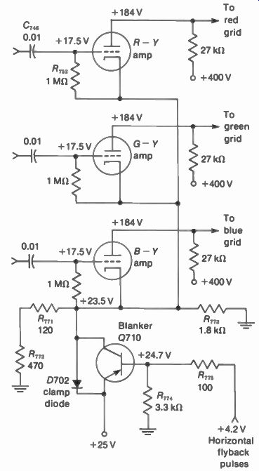
FIGURE 17-29 DETAILS OF BLANKER STAGE. FROM CIRCUIT IN FIG. 17-26. R IN OHMS
AN DC IN MICROFARADS.
Grid-leak bias for the R - Y amplifier, as an example, is produced by the flyback pulses at the cathode from the collector of the blanker stage Q710. Into the base are pulses of positive polarity. Out from the collector are amplified and inverted negative flyback pulses. The negative pulse at the cathode of the R - Y amplifier corresponds to positive grid voltage, to produce grid current. Then the 0.01-µF coupling capacitor C7„; is charged. The RC time constant with the R„, is long enough to maintain the bias between pulses.
In addition, the flyback pulses at the cathode of the color-difference amplifier are amplified but not inverted in the plate circuit.
Then the negative pulses to the control grid of the picture tube cut off beam current during horizontal retrace time. The guns are cut off only for the period of the flyback pulses.
The blanker Q710 is a PNP transistor. V rE is -1.5 V, equal to the difference between 25 V on the emitter and 23.5 V at the collector. The transistor is normally conducting full saturation current, but the positive flyback pulses at the base cut the stage off. Then the collector voltage rises to provide positive flyback pulses at the cathode of each color-difference amplifier.
The clamp diode Q702 prevents the cathode voltage from exceeding 25 V.
17-12 Troubles in the Color Circuits
To save time in localizing troubles, it is important to keep in mind the fact that the ac color signals from all the color circuits have only one function in the overall picture. The color information is important, but it is just superimposed on a monochrome picture formed on a white raster. The gray scale or color temperature of the raster depends on dc voltages for the picture tube. The monochrome picture is produced by the ac luminance signal.
The color information is a result of correct operation of the 3.58-MHz chroma amplifier, 3.58-MHz burst amplifier, 3.58-MHz color oscillator, color AFPC circuit, color demodulators, and color video amplifiers. Normal oscilloscope waveshapes for these ac color signals can be seen by referring back to Fig. 9-4. These waveshapes are obtained by tracing the signal from a color-bar generator.
Is the raster normal? Its gray scale depends on the dc grid bias and screen voltage for each gun in the picture tube. Because of dc coupling from the color video amplifiers, a change in dc voltage here can change the bias for the raster.
In addition, a short circuit from grid to cathode or cathode to heater in the picture tube affects the bias. However, normal gray scale without color in the raster and brightness that can be varied by the brightness control indicate that the picture tube is good and the dc bias voltages are normal.
Is the black-and-white picture normal? This shows normal Y video signal with balanced drive for the red, green, and blue guns. The contrast control should vary the amount of contrast in the picture. A normal monochrome picture on a white raster indicates a good picture tube. See if the screen controls vary the color of the raster.
Is the color picture tube good? The conventional trouble of weak emission from one gun in an old tube shows as a weak, silvery picture for that color. However, even a new picture tube can have internal short circuits that affect the bias and the brightness. This often is indicated by flashing in the picture, with visible retrace lines. The possibility of a cathode-to-heater short can be checked with an isolation-booster transformer for the heater. However, when the monochrome picture is normal on a good raster, any color trouble is not likely to be in the picture tube because its most difficult function is to make a good black-and-white picture.
Dc-voltage troubles. In the picture tube, color video amplifier, or Y video amplifier, any trouble that changes the dc bias for the picture tube affects the gray scale of the raster. Furthermore, a bias trouble can be confused with no high voltage because of no brightness. The screen may be very dark, but any illumination at all shows that high voltage is present.
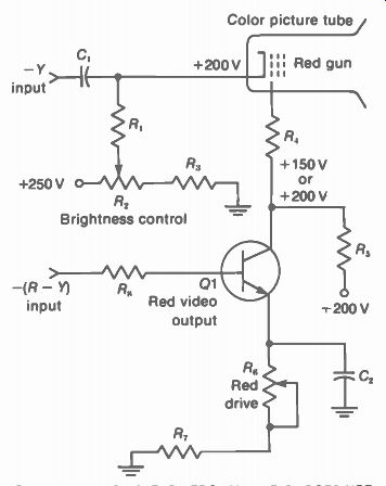
FIGURE 17-30 DC VOLTAGE TROUBLE. IF Q1 DOES NOT CONDUCT, THE GRID OF THE
RED GUN WILL BE TOO POSITIVE.
A dc-voltage trouble that causes excessive color in only one hue is illustrated by the circuit in Fig. 17-30 for a red video amplifier Q1.
The collector voltage of Q1 determines the control-grid voltage for the red gun. The cathode voltage is set by the brightness control at 200 V. Normally, the grid voltage is 150 V. This results from the 50 V drop of /,• across R _p from the 200-V collector supply. The net grid-cathode voltage then is 150 - 200 = -50 V for the control grid.
However, if Q1 is not conducting, its collector voltage rises to 200 V. Then the grid bias is 200 - 200 = 0 V. With zero bias, the red gun conducts maximum current. Since the blue and green guns have only normal bias, the entire screen will be red. Probably the raster will bloom also because of excessive beam current.
This trouble of too much red will be in the raster, monochrome picture, and color picture.
Troubles in the ac color signal. These effects are just in the color; the monochrome picture is normal. The different possibilities are no color at all, weak color, no color sync, wrong hues, and trouble in just one color. These are considered separately in the next sections. Remember that the 3.58-MHz signal is for all the colors.
Only the individual color video signals after the demodulators have separate colors. However, these stages may all be in one common tube or IC unit. Also note that the color video amplifiers in Fig. 17-26 have one common-cathode resistor, which is R77:1 . No color. Check for output in the 3.58-MHz chroma amplifier and oscillator circuits. Make sure the color killer or ACC circuit is not cutting off the bandpass amplifier. Note that if there is no burst signal, the color killer will cut off the chroma signal, either in the bandpass amplifier or in the demodulators.
Color snow. See color plate V. With the color level control at maximum, the color killer off, and the receiver tuned to an unused channel, the screen should show color snow. This is random noise at frequencies near 3.58 MHz that is amplified in the color circuits. The presence of color snow but no color picture shows that the color circuits are operating, but there is no 3.58-MHz chroma signal.
No color sync. See color plate V1. Drifting colors or color bars indicate that the color oscillator is not being synchronized by the color burst signal. The cause is always the AFPC section.
If there is no color sync burst, however, the result will be no color at all, as the color killer cuts off the chroma signal.
One color missing. This symptom is usually caused by a problem in a single color video channel. Keep in mind the hues for the color difference signals. B - Y is essentially blue and yellow; R - Y is red and cyan; G - Y is green and magenta; X signal is close to -(R - Y) with cyan and red; and Z signal is close to -(B - Y) with yellow and blue.
SUMMARY
1. The color circuits in the receiver use the 3.58-MHz modulated chroma signal to provide red, green, and blue video signals for the picture tube.
2. The input to the video preamplifier stage is the colorplexed composite video signal from the video detector. The output supplies Y signal to the delay line into the video amplifier, composite video signal for the deflection sync and AGC stages, plus 3.58-MHz chroma signal for the bandpass amplifier.
3. The Y video amplifier supplies the luminance signal of 80 to 140 V p-p needed to drive the picture tube. The delay line in the input to the Y amplifier delays the luminance signal approximately 0.8 As with respect to the color signal.
4. The 3.58-MHz bandpass amplifier, or color amplifier, supplies chroma signal to the color demodulators. The color amplifier generally has the color level control to vary the saturation in the picture by varying the amount of color signal.
5. The burst amplifier separates the 3.58-MHz color sync burst on the back porch of the horizontal blanking pulses. This is accomplished by keying the stage to be on for horizontal retrace time only.
6. The color oscillator is controlled by a 3.579545-MHz crystal. Its function is to re generate the 3.58-MHz subcarrier suppressed in transmission. The output of the color oscillator, with the phases required to detect the desired hues in the 3.58-MHz modulated chroma signal, goes to the synchronous demodulators.
7. The automatic frequency and phase control (AFPC) circuit locks in the color oscillator to hold the hues steady in the reproduced picture.
8. A color demodulator is a synchronous detector that requires two input signals.
One is the 3.58-MHz modulated chroma signal. The other is 3.58-MHz oscillator cw of a particular phase to detect specific hues in the chroma signal. The detected output is color video signal.
9. The Y video signal and color video signals may be matrixed in the picture tube to produce red, green, and blue video, or the matrixing can be in the color video circuits.
10. Color troubles can be localized in terms of the raster and monochrome picture.
A good raster shows normal dc voltages. A good monochrome picture shows normal Y signal and correct dc voltages for the picture tube. Usually, this indicates that the picture tube is not defective. No color at all results from no ac chroma signal at 3.58 MHz or no oscillator cw output. Troubles with one color are in the ac signal from a color video amplifier. Color sync troubles are generally caused by the AFPC circuit.
Self-Examination (Answers at back of guide)
1. Which of the following is not tuned to 3.58 MHz: (a) burst amplifier; (b) video preamplifier; (c) chroma amplifier; (d) color demodulator input.
2. When 8 - Y and Y signal are combined, the result is: (a) blue video; (b) 3.58-MHz chroma; (c) red video; (d) green video.
3. The phase angle between 8 - Y and R - Y is: (a) 180'; (b) 57'; (c) 0'; (d) 90.
4. Which of the following applies for a monochrome program: (a) chroma amplifier on; (b) Y video amplifier off; (c) color killer on; (d) picture tube off.
5. The manual color control is generally in which circuit: (a) red video output; (b) Y video output; (c) chroma bandpass amplifier; (d) R - Y demodulator.
6. The contrast control is generally in which circuit: (a) burst amplifier; (b) Y video amplifier; (c) blue video output; (d) color oscillator.
7. A manual control in the AFPC circuit is for (a) tint; (b) saturation; (c) contrast; (d) brightness.
8. If the color oscillator does not operate, the result will be: (a) no picture; (b) no color; (c) incorrect hues; (d) no color sync.
9. The hue of the color sync burst phase is: (a) red; (b) blue; (c) magenta; (d) yellow-green.
10. The balance for Y video signals to the three guns in the picture tube is set by the: (a) drive controls; (b) screen controls; (c) contrast control; (d) color control.
Essay Questions
1. Give three requirements for a picture reproduced in color.
2. List the input and output signals for the following stages: video preamplifier, Y video amplifier, chroma bandpass amplifier, burst amplifier, R - Y demodulator, color oscillator, and G - Y adder.
3. Give the circuits and functions for the manual contrast, color, and tint controls.
4. Give two differences between the sets of controls for R, G, B drive and R, G, B screen-grid adjustments.,
5. What is the difference in color synchronization between a ringing oscillator circuit and an oscillator with a reactance tube?
6. Approximately how much video signal voltage is required to drive a 21-in, color picture tube?
7. Give the polarity of Y video signal and color video signal required at the cathode of the picture tube.
8. List the video signals with their polarity for matrixing in the picture tube.
9. Give one advantage and one disadvantage of matrixing in a video stage, before the picture tube.
10. Give one stage in the color circuits that must be conducting during horizontal flyback time and one that is cut off.
11. Draw a phasor diagram, showing two sets of color axes that can be used in the demodulator circuits.
12. Draw frequency response curves for the chroma bandpass amplifier, without compensation for the picture IF amplifier and with compensation.
13. What is the function of the color killer circuit?
14. Make a list of the color circuits that are tuned to 3.58 MHz.
15. In Fig. 17-3, give the functions for T, and R324. How much is the collector-emitter voltage?
16. In Fig. 17-11, what are the functions of 7 - 3, R3„, and Cm?
17. In Fig. 17-15, list the three stages for AFPC and give the function of each.
18. In Fig. 17-20, list the signals into the two demodulators Q1 and Q2.
19. In Fig. 17-28, give the signals into and out of the red video output stage Q1
20. How can the trouble of no color sync burst cause no color in the picture?
21. Give two troubles that can cause no color with a normal monochrome picture.
22. How will the reproduced picture look with no Y video signal?
23. At all three cathodes of the picture tube the bias voltage is 184 V, with 150 V at the control grids. The cathode voltage then shifts to 210 V. How much is the bias now?
24. How does the picture look without color sync?
25. What is the effect of no high voltage for the anode of the color picture tube?
26. Show arrows for the block diagram in Fig. 17-31 below, to indicate the sequence for Y and B - Y signals to the picture tube.
FIGURE 17-31 FOR ESSAY QUESTION 26.