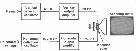
Both the vertical and horizontal deflection circuits produce the scanning raster on the screen of the picture tube, as illustrated in Fig. 21-1. For horizontal scanning, the horizontal oscillator drives the horizontal output stage to produce the scanning lines at 15,750 Hz. At the same time, the vertical oscillator generates 60-Hz deflection voltage to drive the vertical output stage. As a result, the vertical scanning fills the screen from top to bottom with horizontal lines to form the raster. The height depends on the amount of vertical output: the width depends on the horizontal output. The requirements of the horizontal output circuit, with flyback high voltage and the damper stage, are analyzed in the next SECTION. Here we consider just the circuits involved in vertical scanning. These topics include:
21-1 Triode vertical output stage
21-2 Transistorized vertical output stage
21-3 Vertical output transformers
21-4 Vertical linearity
21-5 Internal vertical blanking
21-6 Multivibrator for combined vertical oscillator and amplifier
21-7 Transistorized blocking oscillator and vertical amplifier
21-8 Miller feedback integrator circuit
21-9 Transistor pair in vertical output circuit
21-10 Vertical deflection troubles
FIGURE 21-1 THE VERTICAL AND HORIZONTAL DEFLECTION CIRCUITS PRODUCE THE SCANNING
RASTER ON THE SCREEN OF THE PICTURE TUBE.
21-1 Triode Vertical Output Stage
This is a power amplifier to supply the required amount of sawtooth current. The frequency of the amplifier output is 60 Hz, the same as the drive from the vertical deflection oscillator. With tubes, a triode amplifier is often used because it provides better linearity in the sawtooth current output than a pentode. However, a beam-power pentode with negative feedback can be used to reduce nonlinear distortion. With transistors, a PNP or NPN power transistor in the common emitter circuit corresponds to a triode output amplifier. However, a transistorized circuit needs a driver stage to serve as a buffer and isolate the low impedance of the output stage from the sawtooth generator.
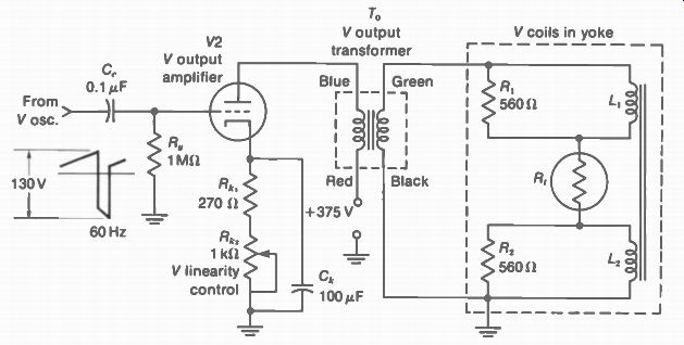
FIGURE 21-2 TRIODE VERTICAL DEFLECTION AMPLIFIER CIRCUIT.
As shown in Fig. 21-2, the main components of the triode vertical amplifier are the power output tube V2 and the stepdown output transformer T. Like an audio output transformer, T„ matches the relatively high impedance with low plate current in the primary to the low secondary impedance and high current needed for the scanning coils in the deflection yoke. Actually, the vertical output stage is an audio power amplifier for the 60-Hz deflecting signal.
Its operation in providing 60-Hz sawtooth current in the vertical deflection coils can be summarized as follows:
1. Trapezoidal voltage from the vertical oscillator provides a linear rise in grid voltage to produce a linear rise in plate current during trace time. When the negative spike on the trapezoidal voltage input drives the grid voltage more negative than cutoff for retrace, the plate current drops to zero. The result is sawtooth plate current.
2. The sawtooth plate current of the amplifier flows through the primary winding of T.
3. The plate-current variations in the primary induce voltage in the T„ secondary that produces sawtooth secondary current.
4. Since the T„ secondary winding is across the vertical deflection coils, they also have saw tooth current.
Referring to Fig. 21-2, C, and R _p couple the 60-Hz trapezoidal voltage from the plate of the vertical oscillator to the grid of the amplifier.
Cathode bias is provided by R _p and R,„, both bypassed by CA. The variable resistance RA, adjusts the amplifier bias to control the linearity of the sawtooth rise in plate current. Minimum bias is provided by F?„, when the linearity control is at zero resistance.
The cathode bias voltage V_ equals I_k. x R _k. If we assume R_k2 is set for 730 ohm the total cathode resistance equals 1,000 ohm. With an average plate current of 30 mA, this is also the cathode current for a triode stage without grid current. Therefore, Vk is 1,000 x 0.03, or 30 V. Normally there is no grid-leak bias on the vertical output stage. The only bias is the cathode voltage, for minimum amplitude distortion in the sawtooth output current. Grid current would limit the peak plate current, causing poor linearity with a white bar at the bottom of the raster.
Typical voltage and current waveshapes for a triode vertical output stage are shown in Fig. 21-3. Note that the negative spike in the trapezoidal grid voltage drives e,. far negative to cut off plate current, even though the plate voltage rises to a high positive value. This rise in e„ is the self-induced primary voltage in T„ when i _p drops to zero for the retrace. The function of the pulse in the trapezoidal waveform, therefore, is to cut off the output stage during retrace time.
The trapezoidal waveshape of the output e _p is an amplified and inverted form of the input e,.. The sawtooth plate current i _p is a fluctuating dc waveform, but the sawtooth current in the secondary is an ac waveform, as only the variations of current are coupled by the transformer.
The shunt damping resistors R, and R, across the vertical scanning coils are in the yoke housing. Their function is to prevent ringing at the start of vertical flyback.
The thermistor R_t is also in the yoke. A typical value is 8 ohm, cold. As the yoke heats up with scanning current, the wire resistance increases but the thermistor resistance decreases to maintain constant height in the raster.
Typical values for a vertical deflection coil are an L of 3.5 to 50 mH, R of 4 to 60 ohm, and saw tooth scanning current of 400 mA to 3 A, peak to-peak. The two coils are usually in series for a vacuum tube amplifier but in parallel for a transistor vertical output circuit.
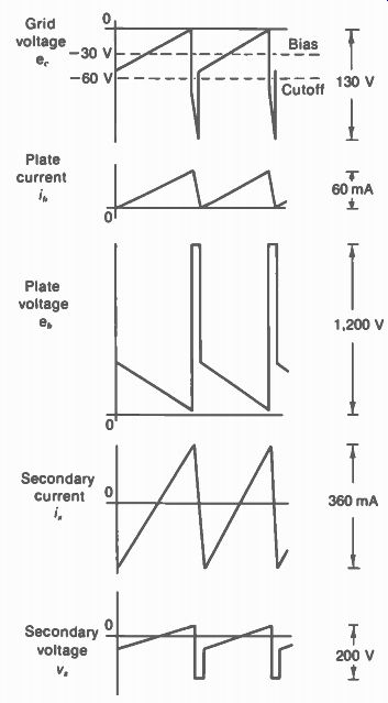
FIGURE 21-3 WAVEFORMS FOR TRIODE VERTICAL OUTPUT CIRCUIT IN FIG. 21-2. FREQUENCY
IS 60 Hz. VOLTAGE OUTPUT SHOWN FOR TURNS RATIO OF 6:1 IN T„ THE POLARITY OF
V, MAY BE INVERTED.
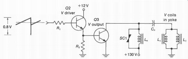
FIGURE 21-4 TRANSISTOR VERTICAL DEFLECTION AMPLIFIER WITH EMITTER FOLLOWER
D2 DRIVING CE OUTPUT STAGE 03.
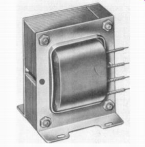
FIGURE 21-5 VERTICAL OUTPUT TRANSFORMER. BASE IS 2 IN. SQUARE. (STANCOR).
21-2 Transistorized Vertical Output Stage
The circuit in Fig. 21-4 has the same function as the triode amplifier in Fig. 21-2, supplying saw-tooth current at 60 Hz to the vertical scanning coils in the deflection yoke. With transistors, though, the driver D2 is a buffer stage to isolate the power amplifier Q3 from the deflection oscillator. D2 is an emitter-follower dc-coupled to the common-emitter (CE) amplifier 03. Both are NPN transistors, requiring positive voltage at the base for forward bias. R, is the emitter load resistance for D2, while the inductance L„ is a choke in the collector output of Q3.
The trapezoidal voltage to the base of D2 is 0.8 V, peak-to-peak. Actually the sawtooth component is only about - ±0.1 V, to drive a transistor between saturation and cutoff. Note the polarity, with a positive-going sawtooth for trace and the negative spikes that produce cutoff for retrace. The polarity out of the emitter of D2 is the same as into the base, because the stage is an emitter-follower. Therefore, the base of D3 has the same polarity of drive voltage as the driver. In the collector output of Q3 the trapezoidal voltage is amplified and inverted by the CE output stage.
Because of the low impedance of the transistor power amplifier Q3, the collector output voltage can be choke-coupled, with L„ as the collector load. C, couples the vertical scanning signal to the yoke coils and blocks the dc collector voltage. A typical value is 500 uF, which requires an electrolytic capacitor. The blocking function is necessary, as any direct current through the deflection coils would move the electron beam off center. The vertical scanning coils L, and L 2 are shown connected in parallel for a transistor output circuit.
The varistor SC1 across the inductance L„ protects the output transistor Q3 against voltage transients in the collector circuit. A varistor provides a short circuit above its breakdown voltage, in either polarity. During retrace, the high positive spike on the trapezoidal voltage output may exceed the collector voltage break- down rating. For the opposite polarity, any transient negative voltage would put forward bias on the collector, causing excessive current.
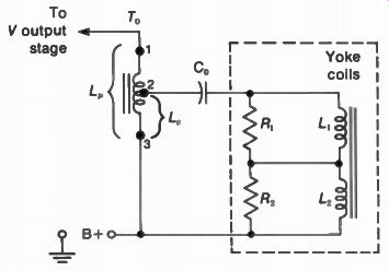
FIGURE 21-6 OUTPUT CIRCUIT AUTO-TRANSFORMER FOR VERTICAL
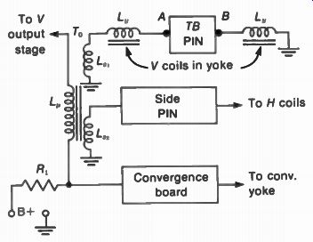
FIGURE 21-7 VERTICAL OUTPUT TRANSFORMER WITH CONNECTIONS OF PIN-CUSHION (PIN)
CORRECTION CIRCUITS FOR COLOR PICTURE TUBE. TB IS TOP AND BOTTOM.
21-3 Vertical Output Transformers
A typical unit is shown in Fig. 21-5. The transformer may have an isolated secondary winding as shown for T in Fig. 21-2, or an autotransformer can be used. With separate windings, any dc voltage in the primary is blocked from the secondary, and so it is not necessary to use a coupling capacitor. With an auto-transformer, however, a capacitor is used to prevent the dc level of the scanning current from the changing the centering of the electron beam.
Common values for the primary L _p are 12 to 40 H, with a turns ratio ranging from 40:1 to 6:1. Typical dc resistances are 500 ohm for L_p , and 6 ohm for L_p. The leads may be color-coded, red for B+ voltage and blue for the plate or collector in the primary, while the secondary wires are green, brown, and black.
Autotransformer for vertical output. In Fig. 21-6, L„ includes all the turns but L, is tapped down on the coil. The result is voltage stepdown and current stepup from primary to secondary.
L _p is between points 1 and 3, while L, is between 2 and 3. The varying current in the primary generates self-induced voltage in all the turns.
Since this is an iron-core transformer with unity coupling, the voltage and current ratios are proportional to the number of turns from 1 to 3 for L _p and from 2 to 3 for L _p the same as with a separate secondary winding. However, the B- voltage for the primary of the autotransformer is not isolated from the secondary. The deflection coils in the yoke then have B+ voltage. C„ blocks the path for direct current, though, to prevent a shift in vertical centering.
Vertical output connections for color picture tubes. Scanning is not related to picture in formation. However, color picture tubes need dynamic correction for pincushion distortion, because permanent magnets cannot be used. The pincushion (PIN) circuits are usually on a separate board, but they are connected to the vertical deflection coils in the yoke to modify the scanning with a waveform that compensates for the pincushion distortion. In addition, although the convergence circuits are on a separate board, they need the vertical signal from the output circuit for dynamic convergence correction at the top and bottom of the picture.
In Fig. 21-7, note that the pincushion correction circuits for the top and bottom (TB) of the raster are directly in series with the two vertical deflection coils in the yoke. This connection means that troubles in the TB pincushion circuits can affect the vertical scanning. To localize this problem, the two connections at points A and B can be shorted temporarily to check the vertical scanning without the TB pin cushion circuits.
The vertical output transformer T„ also has a separate winding L„ to provide vertical scanning signal to the pincushion correction circuits' for the left and right sides of the raster.
However, these connections are separate from the vertical scanning coils. In addition, the saw tooth voltage across R, in the output circuit is used for vertical dynamic convergence' at the top and bottom of the picture.
[Pincushion correction and dynamic convergence circuits are described in Section 11. ]
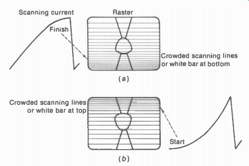
FIGURE 21-8 VERTICAL NONLIN EARITY (a) FLAT FINISH ON SAW TOOTH CAUSES CROWDING
AT BOT TOM OF RASTER, (b) FLAT START ON SAWTOOTH CAUSES CROWDING AT TOP OF
RASTER . Crowded scanning lines or white bar at top; Crowded scanning lines
or white bar at bottom
21-4 Vertical Linearity
Nonlinear vertical scanning is more noticeable than horizontal nonlinearity because we can easily see the effects. When a person's head is too flat, this means the scanning lines at the top are compressed or crowded together. Stretching the scanning lines at the top makes the head too long. At the bottom, stretching or compressing the lines can make a person's legs too long or too short. With a test pattern, the top and bottom wedges can be too short or too long, as in Fig. 21-8. Also, circles are distorted.
The three main factors affecting linearity of the vertical scanning are:
Flat finish toward the end of the sawtooth waveform, as in Fig. 21-8a. This can result from using too much of the RC charge curve, from a short time constant, or from a leaky sawtooth capacitor.
2. The same type of nonlinear distortion can be caused by saturation in the iron core of the vertical output transformer or by a weak amplifier.
3. The input-output operating characteristic of the vertical output amplifier usually has the opposite distortion shown in Fig. 21-8b, with a flat start on the sawtooth waveform.
Remember that the finish of the sawtooth at the top of the waveform corresponds to the bottom of the raster, just before retrace. The start of the sawtooth waveform is the top of the raster. By adjusting the operating characteristic of the vertical amplifier, the two opposite curvatures in Fig. 21-8 can be made to balance each other for linear scanning. For this reason, the vertical linearity control is in the vertical output circuit to adjust the operating characteristic. In Fig. 21-2, the vertical linearity control varies the cathode bias on the vertical amplifier. Any method of varying the bias affects the linearity of the vertical amplifier. Another common method of adjusting linearity is to adjust the amount of feedback in the vertical circuit.
Since the linearity control changes the gain of the vertical amplifier, it also changes the height. Similarly, the height control in the oscillator circuit changes linearity. Both controls should be adjusted together to fill the screen top to bottom with uniform spacing of the scanning lines. It can be useful to note that the linearity control generally will stretch the top more than the height control, which stretches the bottom.
A common problem is that the height control cannot pull the bottom of the raster down enough. Then good linearity can only be obtained with too little height. Or, the correct height can be produced only with stretching at the top. This trouble is really insufficient height, with weak vertical output, rather than poor linearity. With tubes, try a new vertical amplifier.
For actual linearity troubles, check for the correct dc operating voltages on the vertical output stage and for a leaky coupling capacitor.
Vertical linearity can be checked by using a bar generator. With about 10 to 20 horizontal bars across the screen, adjust for uniform spacing. Another method is to check the width of the black horizontal blanking bar across the screen as it drifts up or down. Turn the vertical hold control slightly off frequency to make the picture roll slowly. Incidentally, the picture will usually roll when the vertical linearity and height controls are varied, but this is no problem as long as the picture can be locked in with the vertical hold control.
21-5 Internal Vertical Blanking
The voltage pulse produced during flyback in the vertical output circuit is coupled to the picture tube for the purpose of providing additional blanking during vertical retrace time. The circuit is also called a retrace suppressor. This is in addition to the blanking voltage at the grid cathode circuit of the picture tube, which is part of the composite video signal. The advantage of the added blanking voltage is that the retrace lines produced during vertical flyback do not appear on the screen for any setting of the bright ness control.
Actually, internal vertical blanking must be used in receivers that do not have the dc component of the video signal at the picture tube. Otherwise, the vertical retrace lines would show when the background in the picture changed for a darker scene. Just about all receivers use a vertical retrace suppressor circuit. Color receivers usually have a horizontal retrace suppressor circuit also.
The vertical flyback pulse for blanking can be either applied to the picture tube or injected into the video amplifier. At the picture tube, the required amplitude is 50 to 150 V to cut off beam current. The polarity for blanking is positive at the cathode, as shown in Fig. 21-9a. The inverted trapezoid in Fig. 21-9b has negative voltage spikes for vertical blanking at the control grid or the screen grid. In both coupling circuits, C blocks any dc voltage.
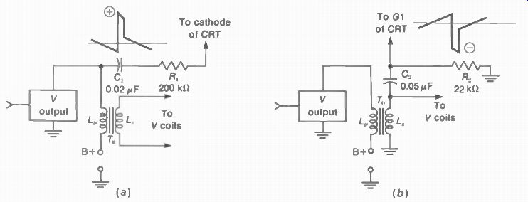
FIGURE 21-9 CIRCUITS FOR INTERNAL VERTICAL BLANKING. (a) POSITIVE RETRACE
PULSES FROM PLATE OF OUTPUT TUBE: (b) NEGATIVE RETRACE PULSES FROM TRANSFORMER
SECONDARY.
When the flyback pulses for blanking are injected into the video amplifier, the required amplitude is only a few volts. This method is often used in transistor receivers. In color receivers, a separate blanker stage is generally used to amplify both vertical and horizontal flyback pulses, which are coupled into the video amplifier for blanking.
The methods of obtaining the vertical flyback pulses for internal retrace blanking include the following:
1. From plate or collector of vertical output stage (Fig. 21-9a). The polarity of the flyback pulse here is positive at the plate of a tube or at the collector of an NPN transistor.
2. From secondary of output transformer (Fig. 21-9b).
3. From a separate winding on the output transformer for vertical blanking.
4. From the spiking resistor in series with the sawtooth capacitor in the vertical oscillator circuit. This method provides a sharp peak alone, without the sawtooth, but the amplitude is low compared with the output circuit.
The RC network for coupling the vertical retrace pulses has two functions: (1) block dc voltage; and (2) flatten the sawtooth tilt. Otherwise, the sawtooth voltage can modulate the beam intensity to vary the shading in the picture from top to bottom.
It should be noted that the retrace suppressor circuits provide a connection that links the deflection circuits with the picture tube and its video signal circuits. A trouble in the retrace suppressor, or the blanker stage, can affect the picture.
21-6 Multivibrator for Combined Vertical Oscillator and Amplifier
As illustrated in Fig. 21-10, a free-running, plate coupled, unsymmetrical MV can be used for the complete vertical deflection circuit. Only one dual-section tube is necessary in the MV, and the feedback from the output circuit eliminates the need for a blocking oscillator transformer.
Either a dual-triode or a triode-pentode is used.
Common dual-triodes in this circuit are the 8CG7. 10DR7, 13EM7, and 15FM7, for series heaters. Triode-pentodes often used are the 21LR8 and 25J28. The pentode section is the output stage. The pentode output is preferred with lower values of B± supply voltage.
In Fig. 21-10, the plate of V1 drives the grid of V2 through an RC coupling circuit, and the plate of V2 is coupled to V1 through the R,C, feedback circuit. Conduction in V1 cuts off V2.
Then conduction in V2 cuts off Vi. The MV is unsymmetrical, as V2 conducts for a longer time to supply sawtooth output current for the trace.
Then V1 conducts for a short time to cut off V2 for the retrace. The sawtooth capacitor is in the plate circuit of V1, serving as the discharge tube.
A pentode for V2 in the vertical output stage usually has negative feedback from plate to its own grid to improve linearity.
The circuit in Fig. 21-10 can also be considered as V1 for a blocking oscillator with feedback from the amplifier V2.
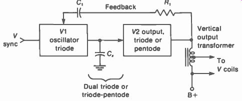
FIGURE 21-10 DUAL-SECTION TUBE AS PLATE-COUPLED MV FOR VERTICAL DEFLECTION.
The schematic diagram of this MV circuit for vertical scanning is shown in Fig. 21-11 with the 15FM7 dual-triode. The V9A section at the left serves as the vertical deflection oscillator, while the V9B section is the vertical amplifier.
The autotransformer T„ supplies sawtooth output current to the vertical deflection coils. The variable cathode resistance R. varies the bias on V9B to control the linearity of the sawtooth output.
In the plate of V9A from R, the 0.1 uF C _p is the sawtooth capacitor, charging toward + 695 V while V9A is cut off. The height control R20 varies the RC time constant on charge to adjust the sawtooth amplitude. This voltage drive is coupled to the grid of V9B by C42 and R23. In the output circuit, the plate of V9B provides feedback through C„, Al, and C,„ to the grid of V9A. The printed circuit A1 is a compact unit with series resistances and shunt capacitances to shape the feedback voltage. In the grid circuit of V9A, the vertical hold control R2, varies the RC time constant, which deter mines the cutoff time, to adjust the frequency.
Vertical sync voltage from the A2 integrator is applied to the plate of V9A or the grid of V9B. The sync polarity is negative to reduce the output plate current of V9B, which increases its plate voltage. This positive feedback to the grid of V9A triggers V9A into conduction to start the vertical retrace.
The waveshapes in Fig. 21-11b show trapezoidal voltage drive at the grid of the vertical amplifier, with a peak-to-peak amplitude of 160 V. In the plate circuit, this trapezoid is amplified and inverted with 680-V amplitude. The positive spike in the plate circuit results from the high value of self-induced voltage produced across the output transformer T, when the plate current is cut off. Since the plate voltage of V9B is fed back to V9A, the spike is also in the trapezoidal plate voltage of V9A. This negative spike in the plate circuit of V9A is a flyback pulse that is coupled by C„, to the screen grid of the picture tube for vertical retrace blanking.
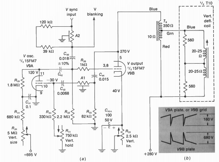
FIGURE 21-11 DUAL-TRIODE AS PLATE-COUPLED MV FOR VERTICAL OSCILLATOR AND
OUTPUT STAGES. R IN C IN µF. A1 AND A2 ARE PRINTED-CIRCUIT RC INTEGRATORS.
ARROW ON CONTROLS INDICATES CLOCKWISE ROTATION. (a) CIRCUIT; (b) TRAPEZOIDAL
VOLTAGE WAVESHAPES. (FROM ZENITH CHASSIS 14M29)
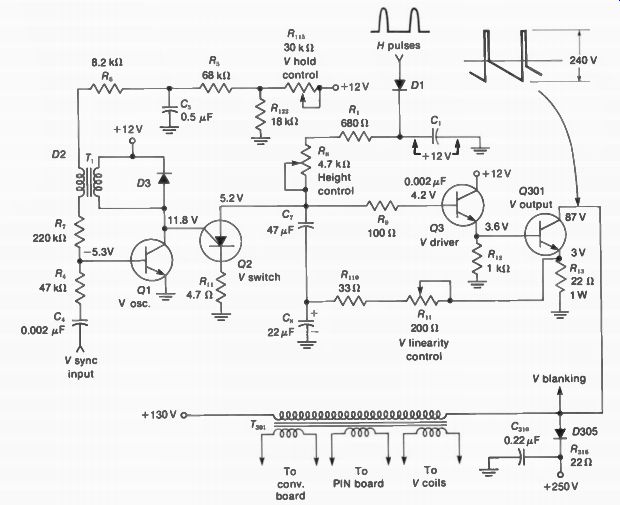
FIGURE 21-12 TRANSISTORIZED BLOCKING OSCILLATOR WITH EMITTER-FOLLOWER AND
CE VERTICAL AMPLIFIER. (FROM MAGNAVOX CHASSIS T979)
21-7 Transistorized Blocking Oscillator and Vertical Amplifier
See Fig. 21-12. 01 is a blocking oscillator, synchronized at 60 Hz by the vertical sync input.
Q2 is a silicon controlled rectifier (SCR) that serves as a switch to discharge the sawtooth capacitance, consisting of C. and C„ in series.
The collector output voltage of Q1 drives the gate electrode of D2. The sawtooth voltage output is directly coupled to the base of Q3.
This stage is an emitter-follower with high input impedance that isolates the oscillator and switch from the low impedance of the vertical output stage Q301. This is a CE (common emitter) amplifier.
In the Q1 circuit, T, is the blocking oscillator transformer which supplies feedback from collector to base. The negative dc voltage of -5.3 Vat the base results from the positive feed back voltage from the transformer, producing base current and reverse bias, similar to the grid-leak bias with a tube. C, and the series resistance in the base circuit provide the RC time constant for discharge of the reverse bias, which determines the free frequency. The vertical hold control 13115 varies the RC time constant and the amount of positive base voltage from the +12-V supply to control the frequency of the oscillator. Positive sync voltage from the sync separator and vertical integrator is coupled to the base by C4 to trigger the oscillator at 6C Hz.
In the vertical switch Q2, the gate voltage determines when the SCR conducts between anode and cathode. The collector output of Q1 is a series of positive pulses at 60 Hz to gate Q2 on.
Without the gate pulse, the SCR is off. Then C, and C„ can charge. The charging voltage is obtained from the 12 V across C, as a dc source.
This equivalent voltage source is produced by horizontal flyback pulses coupled by D1 to charge C,. These pulses are positive, charging C, to a positive 12 V. The time constant for charging the saw tooth capacitors C 7 and C„ is varied by the height control R„, to adjust the sawtooth amplitude.
The resulting sawtooth voltage is directly connected to the base of the vertical driver Q3.
The reason for dividing the sawtooth capacitance of C7 and C5 is to provide feedback at the junction, from the emitter of the vertical amplifier, to improve the linearity of the saw tooth rise. The linearity control R„ varies the amount of feedback.
The reason for using horizontal flyback pulses to provide the dc voltage across C, for charging the vertical sawtooth capacitors is to make the vertical output dependent on the horizontal scanning amplitude. If excessive load current reduces the horizontal scanning width, then the vertical height will also decrease.
In the vertical driver Q3, the emitter-load resistance is R _p. This is an emitter-follower, without any ac load impedance in the collector circuit. Note the base-emitter bias of 4.2 - 3.6 = 0.6 V positive at the base of a silicon NPN transistor serving as a linear amplifier.
There is no polarity inversion in an emitter follower. Here, the waveform is a positive-going sawtooth voltage from the switch D2 into the base of Q3 and out from the emitter to drive the base of the output amplifier Q301. This voltage is amplified and inverted to produce the trapezoidal voltage output shown at the collector with a peak-to-peak amplitude of 240 V. In the vertical amplifier 0301, the saw tooth current output is transformer-coupled by T„„ to the vertical scanning coils in the deflection yoke. In addition, separate windings are used for vertical deflection signals to pincushion circuits on the deflection board and to the convergence correction circuits on a separate panel. Also, the output from the collector of Q301 goes to a blanker stage on the video amplifier board for vertical retrace blanking.
The unbypassed resistance R,„ has 3-V emitter bias for Q301 and sawtooth voltage that is fed back to C„, through R _p„ and the linearity control R. The net bias from base to emitter is 3.6 - 3.0 = 0.6 V for this silicon transistor, positive at the base for NPN. The vertical output stage 0301 is a 25-W power transistor in a metal TO-3 case with a heat sink. Supply voltage for the collector is +130 V. However, the self-induced voltage in the primary of T.,„ produces a flyback pulse of 240 V. The diode D305 in the line to +250 V protects the collector against higher transient voltages, which can be more than the breakdown voltage rating. D305 is biased off by +250 V at the cathode. Any voltage more than 250 V at the diode anode and 0301 collector, however, makes the diode conduct. Then the collector is clamped at 250 V.
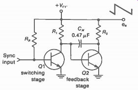
FIGURE 21-13 BASIC CIRCUIT OF MILLER PEEDBACK IN TEGRATOR FOR LINEAR SAWTOOTH
OUTPUT PRODUCED BY C+.
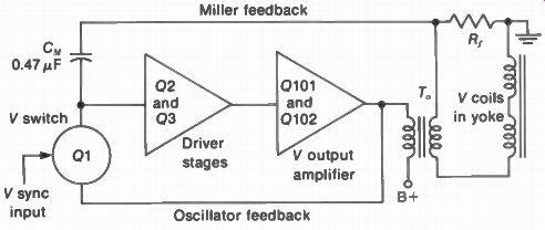
FIGURE 21-14 BLOCK DIAGRAM OF VERTICAL DEFLECTION CIRCUIT USING MILLER FEEDBACK
INTEGRA TOR WITH C„ (FROM RCA CHASSIS CTC49)
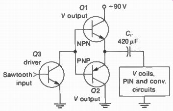
FIGURE 21-15 BASIC CIRCUIT FOR A TRANSISTOR PAIR AS PUSH-PULL VERTICAL OUTPUT
STAGE. NPN AND PNP TRANSISTORS IN COMPLEMENTARY SYMMETRY PROVIDE PUSH-PULL
OUTPUT
21-8 Miller Feedback Integrator Circuit
One problem with a vertical sawtooth voltage generator in transistor circuits is the need for a large, electrolytic sawtooth capacitor because of the low shunt resistance. One solution is to use the feedback circuit with the Miller integrating capacitor C„ illustrated in Fig. 21-13. Q2 represents an amplifier with feedback from output to input, usually including several stages. C„ is a 0.47-µF paper capacitor in the feedback path.
Q1 is directly coupled to Q2 in order to serve as a switch that controls the collector voltage of Q2. The sync input to Q1 reduces its /, to increase If in Q2. When the collector voltage of Q2 decreases with more /,., the feedback capacitor C„ discharges. The result is a negative going sawtooth for the output of Q2, as shown at the collector. This sawtooth voltage has very low amplitude of the order of millivolts, but is extremely linear.
The name "Miller integrator" indicates two important effects. In general, for any amplifier, the Miller effect means that the input capacitance is multiplied by the gain of the amplifier. As a result, a relatively small capacitance in the input circuit can be equivalent to a much larger capacitance, multiplied by a factor as high as 100. An integrating circuit has the characteristic that the rate of change in the output is proportional to the amount of input. In Fig. 21-13, the voltage change across C„ as it discharges is very linear because the amount of discharge current is kept constant by the varying resistance of Q2 in the discharge path. Cw charges through Q1 but discharges through Q2.
A practical vertical deflection circuit using the Miller integrator principle is illustrated by the block diagram in Fig. 21-14. Q101 and Q102 are a pair of power transistors in the vertical deflection output circuit. Q2 and Q3 are amplifiers to drive the power output stage. All the amplifier stages are in the feedback loop, from the secondary of the output transformer through C„ and back to the input of Q2. In addition, the feedback to the switch Q1 makes the circuit free-running. The adjustments for this circuit include a height control and vertical hold for frequency control, but there is no vertical linearity control.
21-9 Transistor Pair in Vertical Output Circuit
Two transistors are often used in push-pull to provide the power output required for vertical deflection. Furthermore, transistor circuits can be arranged without the need for a center tapped push-pull output transformer. One method uses PNP and NPN transistors in a complementary-symmetry output stage (Fig. 21-15). Another method uses a pair of NPN power transistors for the output stages, but the driver stages are opposite transistor types (a circuit called quasi-complementary symmetry).
These push-pull circuits are similar to the audio output stages in high-fidelity amplifiers.
In Fig. 21-15 the collector of the NPN transistor Q1 uses + 90 V for V, Q1 and Q2 are in series across the 90-V supply. Therefore, the dc voltage at the emitter of Q1 serves as the emitter voltage for Q2. The supply voltage is inverted for the Q2 collector, since positive voltage at the emitter corresponds to negative collector voltage for this NPN transistor. The output deflection signal to the vertical deflection coils is taken from the junction of the emitters for Q1 and Q2.
The 470-uF C, blocks any dc voltage from the vertical scanning coils, which would shift the centering.
The push-pull action of Q1 and Q2 results because they have opposite drives. Assume a positive-going sawtooth rise into the driver Q3, resulting in negative drive during trace time at the base for both Q1 and Q2. Since Q1 is PNP with an N base, this driving signal increases the collector current. At the base of Q2, however, the negative drive reduces the forward voltage at the base for less collector current in the NPN transistor.
A push-pull stage can be operated class B or AB for greater efficiency, compared with class A. However, good regulation in the power supply is necessary. Each transistor supplies one half the ac cycle of sawtooth current in the yoke.
One transistor is effective in scanning the top half of the raster, and the other half is produced by the opposite transistor. Figure 21-16 shows a vertical output module board with push-pull transistors.
21-10 Vertical Deflection Troubles
These include stretching and compression at the top or bottom, not enough height, or just a horizontal line across the screen. You can see the troubles in the raster and in the picture.
Horizontal line only. Just a bright line or bar across the middle of the screen, as in Fig. 21-17, means there is no output from the vertical deflection circuits. Often, you can see dark and light picture information moving across the line, which shows video signal is present. This effect of no height can be caused by trouble in any stage of the vertical deflection circuits, including the oscillator, driver, and output stages.
Insufficient height. This trouble is generally caused by a weak amplifier in the vertical output circuit. As shown in Fig. 21-18, the screen has black bars at the top and bottom. These areas are not scanned and, therefore, not illuminated.
The reduced height can also be caused by reduced dc supply voltage for the vertical amplifier.
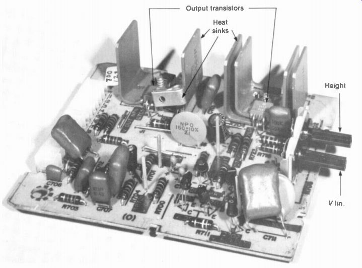
FIGURE 21-16 VERTICAL OUTPUT MODULE BOARD WITH PUSH-PULL TRANSISTORS WIDTH
IS 6 IN (GE)
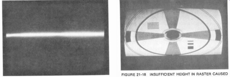
FIGURE 21-17 NO VERTICAL DEFLECTION.
FIGURE 21-18 INSUFFICIENT HEIGHT IN RASTER CAUSED BY WEAK VERTICAL OUTPUT
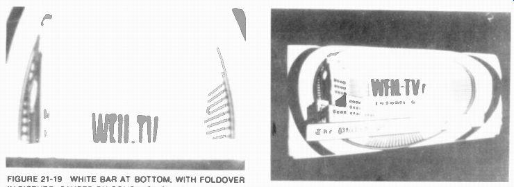
FIGURE 21-19 WHITE BAR AT BOTTOM, WITH FOLDOVER IN PICTURE. CAUSED BY COMPRESSION
AT END OF SAW TOOTH WAVE FOR VERTICAL SCANNING.
FIGURE
21-20 TRAPEZOIDAL RASTER. WITH KEYSTONING CAJSED BY SHORT ACROSS ONE VERTICAL
COIL IN YOKE
White bar across bottom. This effect, shown in Fig. 21-19, is actually an extreme case of vertical nonlinearity. The end of the sawtooth trace is too flat, compressing lines at the bottom to form the white bar. With a picture, the information at the bottom is folded over. This trouble is generally caused by a weak output tube or incorrect bias. A common problem is a leaky coupling capacitor, which shifts the bias. As another cause, a low value of dc supply voltage can reduce the peak sawtooth current needed to pull the scanning down to the bottom of the screen.
Vertical jitter. This trouble is really in vertical synchronization, and caused by noise. We assume the AGC is normal and there is no overload distortion of the vertical sync. The jitter results because the picture starts to roll slightly but is then locked in by the vertical sync.
The problem of horizontal flyback pulses coupled into the vertical deflection oscillator can also produce poor interlacing. To correct this problem of crosstalk between the horizontal and vertical circuits, check the lead dress, make sure the cover is on the high-voltage cage in the horizontal output circuit, and check the RC decoupling filters in the vertical oscillator.
Opens and shorts in the vertical scanning coils. When the two coils are in series, an open in one means no deflection and no height. With parallel coils, one section can affect the top or bottom part of the raster. Shorted turns in either coil, however, produce a trapezoidal raster (Fig. 21-20). Any form of trapezoidal distortion is practically always caused by a defective yoke, or by a trouble in the pincushion correction circuits in color receivers.
Oscillator frequency troubles. If the hold control cannot make the picture roll both Lp and down, the free frequency cannot be set to 60 Hz.
The trouble can be a defective oscillator stage but is often in the RC time constant of cc bias voltage for the oscillator. When you see two or three complete pictures, the oscillator frequency is at 30 Hz or 20 Hz. For 120 Hz and above, you can see the bottom part of the picture folded over the top.
SUMMARY
1. The vertical deflection circuits consist of an oscillator synchronized at 60 Hz driving the power output stage coupled to the vertical scanning coils in the deflection yoke.
2. The height or vertical size control varies the amount of drive to the output amplifier to control the height of the raster.
3. The vertical linearity control either varies the bias in the vertical output stage or adjusts the feedback.
4. Both the linearity and height controls are adjusted fo fill the screen top to bottom with equally spaced scanning lines.
5. For internal retrace blanking, the vertical flyback pulses are coupled either to the picture tube or to the video amplifier to cut off beam current during vertical re trace time.
6. With tubes, the plate-coupled multivibrator shown in Fig. 21-11 is generally used for the vertical deflection circuit. A dual-triode or triode-pentode serves as the oscillator and power amplifier.
7. With transistors for vertical deflection, a typical circuit includes a blocking oscillator and emitter-follower driving the power output stage (Fig. 21-12).
8. In transistorized vertical deflection circuits, the Miller feedback integrator in Fig.
21-14 is often used. This circuit allows a smaller sawtooth capacitor, with good linearity. Usually, there is no linearity control.
9. The vertical output stage may use PNP and NPN transistors in complementary symmetry (Fig. 21-15). This circuit is a push-pull amplifier, similar to the power output stage in audio circuits.
10. With tubes in the output stage, the vertical scanning coils are in series. With transistors, the vertical coils are usually in parallel.
11. In color receivers, the vertical output feeds the pincushion (PIN) correction circuits and convergence correction circuits. The PIN circuits are in series with the vertical scanning coils.
12. Troubles in the vertical deflection circuits affect the height of the raster. Two common troubles: (a) just a horizontal line as in Fig. 21-17, caused by no vertical output; (b) insufficient height as in Fig. 21-18, caused by weak vertical output.
Self-Examination (Answers at back of guide)
1. The voltage waveshape in the output of the vertical amplifier is a (a) trapezoid; (b) sawtooth; (c) rectangle; (d) square.
2. An autotransformer in the vertical output circuit: (a) steps up the voltage for the scanning coils; (b) isolates the scanning coils for B + voltage in the primary; (c) isolates the oscillator and output stages; (d)does not isolate the secondary from dc voltage in the primary.
3. Vertical flyback pulses at the plate of the vertical output tube are for retrace blanking at the picture tube: (a) cathode; (b) control grid; (c) screen grid; (d) anode.
4. The top of the picture is stretched with too much height. To correct this: (a) vary the vertical hold control; (b) reduce height with the vertical linearity control; (c) increase height with the size control; (d) replace the vertical oscillator tube.
5. The vertical deflection circuit in Fig. 21-11 is a: (a) plate-coupled multivibrator; (b) cathode-coupled multivibrator; (c) driven blocking oscillator; (d) Schmitt trigger.
6. In Fig. 21-11, during vertical trace time: (a) the oscillator section V9A conducts; (b) the amplifier section V9B is cut off; (c) V9B conducts; (d) the sawtooth capacitor discharges.
7. In Fig. 21-12, the forward bias between base and emitter of the vertical output stage Q301 equals: (a) 3.0 V; (b) 3.6V; (c) 0.6V; (d) 130 V.
8. Peak-to-peak sawtooth scanning current in the vertical coils can be: (a) 0.7 mA; (b) 0.7 A; (c) 50 A; (d) 150 µA.
9. A push-pull amplifier in the vertical output circuit: (a) usually operates class C; (b) can use PNP and NPN transistors; (c) cannot be used; (d) generally uses two beam power pentodes.
10. In the transistorized vertical deflection circuit in Fig. 21-12, if R. in the emitter of Q301 opens, the result will be: (a) poor linearity; (b)vertical rolling; (c) pincushion distortion; (d) just a horizontal line across the center of the screen.
Essay Questions
1. Describe briefly how the scanning raster is produced. Which stages determine height? Which stages determine width?
2. Why can the deflection circuits produce the raster with or without sync?
3. How is the vertical oscillator synchronized at 60 Hz with (a) positive sync; (b) negative sync?
4. Why does the plate current of the vertical output tube have the sawtooth waveshape?
5. Give two requirements of the vertical output transformer.
6. List three controls for vertical deflection, giving the function of each, and describe briefly how to adjust them.
7. Draw the schematic diagram of a triode output stage, with autotransformer coupling to the vertical deflection coils. Include internal vertical blanking for the picture tube. Give typical values of components. Show voltage waveshapes with typical amplitudes at grid, at plate, and across yoke coils.
8. Give two component troubles that can cause a white bar at the bottom of the raster, with insufficient height.
9. Give two component troubles that can make the oscillator frequency too high.
10. Give two component troubles that can cause no vertical scanning, with just a white line across the center of the screen.
11. What is the function of a thermistor in the deflection yoke?
12. What is the function of a varistor at the collector of the vertical output stage?
13. In the vacuum tube circuit in Fig. 21-11, give the function for each of the following components: C1 „, C4 _p C„, R2„, T _p A2, R20r R21, and A22.
14. In the transistor circuit in Fig. 21-12, give the function for each of the following components: C _p 7 . 1 , D3, Q2, C1, R12, R1 3, Rir„ Rs, and R11.
15. Give one advantage of the Miller feedback circuit for vertical deflection.
16. Refer to the transistor pair for push-pull output in Fig. 21-15. Why would the collector-emitter voltage of D2 be -45 V when the emitter voltage of 01 is +45 V to chassis ground?
Problems (Answers to selected problems at back of guide)
1. How much cathode bias voltage is produced by an R„ of 2,000 II with an average cathode current of 20 mA?
2. Referring to the transistor circuit in Fig. 21-12, how much is the emitter current for: (a) Q3; (b) Q301.
3. Vertical scanning coils have an inductance of 40 mH with R of 50 ohm. Calculate the inductive reactance for a sine-wave current at 60 Hz.
4. Horizontal scanning coils have an inductance of 10 mH with R of 12 ohm. Calculate the inductive reactance for a sine-wave current at 15,750 Hz.