The horizontal output stage is a power amplifier which supplies the scanning current needed in the horizontal deflection coils to fill the width of the raster. Since the horizontal output circuit is primarily inductive, it can also generate flyback pulses of 18 kV or more. This voltage is used for the high-voltage rectifier that produces anode voltage for the picture tube. Furthermore, the high value of self-induced voltage makes the output circuit oscillate. To control this sine-wave ringing, a diode damper is used in the horizontal output circuit. The operation of the horizontal amplifier must be considered along with the damper, as both stages are needed to produce horizontal scanning. It is important to remember that without horizontal scanning there is no high voltage and no brightness. More details of the horizontal output circuit are described in the following topics:
22-1 Functions of the horizontal output circuit
22-2 The horizontal amplifier
22-3 Damping in the horizontal output circuit
22-4 Horizontal scanning and damping
22-5 Boosted B+ voltage
22-6 Flyback high voltage
22-7 Horizontal deflection controls
22-8 Deflection yokes
22-9 Horizontal output transformers
22-10 Analysis of horizontal output circuit
22-11 Complete horizontal deflection circuit
22-12 Protective bias on horizontal output tube
22-13 Transistorized horizontal deflection
22-14 SCR horizontal output circuit
22-15 High-voltage limit control
22-16 Troubles in the horizontal deflection circuits
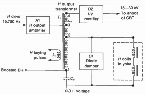
FIGURE 22-1 BLOCK DIAGRAM OF HORIZONTAL OUTPUT CIRCUIT.
22-1 Functions of the Horizontal Output Circuit
As shown in Fig. 22-1, the essential stages are the amplifier, damper diode, and high-voltage rectifier, operating with the horizontal output transformer (H OT.). This is also called the flyback transformer. These stages can use either tubes or transistors and semiconductor diodes. Also, the output stage can use semiconductor switching devices, such as the SCR or gate-controlled switch.
Typical beam-power pentodes for the horizontal amplifier are the 6D05, 171306, and 6G W6 octal tubes with a top cap for the plate connection. The 6JR6, 22JR6, 6L06, and 24L06 are examples of tubes with a novar base and no top cap. Typical diode damper tubes are the 6AX4, 6CL3, 12CL3, 17CT3, and 25CM3. In addition, pentode-diode types such as the 33GY7 and 38HE7 combine the horizontal amplifier and damper in one envelope.
Horizontal scanning. The output stage is a power amplifier which supplies 1 to 5 A p-p scanning current in the yoke coils. In Fig. 22-1, the winding between terminals 3 and 1 is the primary on the autotransformer 7 - 1. The winding between 2 and 1 is the secondary for voltage stepdown and current stepup to the horizontal scanning coils.
Horizontal damping. The damper D1 has the primary purpose of damping sine-wave oscillations, or ringing. Immediately after the fast flyback, the diode conducts to serve as a low shunt resistance that stops the ringing of the inductance. Damping is needed because the oscillations produce white vertical bars at the left side of the raster. It should be noted, though, that the damper does not conduct during re trace. At this time, damping is not desired, in order to allow a fast flyback and maximum amount of high voltage.
Using the damper for scanning. For greater efficiency, the damped output current is used to produce about one-third of the horizontal trace at the left side of the raster. During this time, immediately after flyback, the damper conducts but the amplifier is cut off. The average amplifier current is reduced appreciably, therefore, improving the efficiency. Since the damped current produces part of each horizontal trace, both the damper and amplifier stages are needed for horizontal deflection. This system is often called reaction scanning, and the damper is an efficiency diode.
Boosted B+ voltage. When the damper con ducts, its current charges C„ in Fig. 22-1. This capacitor is in series with D1 and the supply voltage. As a result, the voltage across C„ becomes higher than B+ by the amount of deflection voltage rectified by the damper. As an example, 280 V for B+ can be boosted to 550 V across C„. Or, 140 V for B+ can be boosted to 300 V. This boosted B-+ is the plate supply voltage for the horizontal amplifier tube, which is the reason why the damper must be operating for there to be horizontal output. In fact, all the tubes in the vertical and horizontal deflection circuits generally use boosted B+ for higher plate voltage.
Scan rectification. In solid-state receivers, part of the horizontal output is rectified to provide dc operating voltages. These include screen-grid voltage for the picture tube and collector voltage for the transistors. In this case, it should be noted that the signal circuits depend on the horizontal output for dc supply voltage.
Flyback high voltage. The high-voltage pulse produced across the primary of the horizontal output transformer is stepped up, rectified, and filtered to provide anode voltage of 15 to 30 kV for the picture tube. In Fig. 22-1, the turns of L„ between terminals 3 and 4 are the high-voltage winding for D2. It should be noted that the high voltage rectifier is the only stage conducting in the horizontal output circuit during retrace time.
Although not shown here, the high-voltage supply can also include a circuit to provide about 5 kV to the focus grid in a color picture tube. There may be a separate focus rectifier or the focus voltage can be tapped down on the anode supply.
Horizontal keying pulses. The horizontal output transformer usually has one or more auxiliary windings, indicated by L , in Fig. 22-1, to supply flyback pulses at the horizontal rate. These pulses are used for the AGC circuit, retrace blanking, horizontal AFC stage, and in the color circuits.
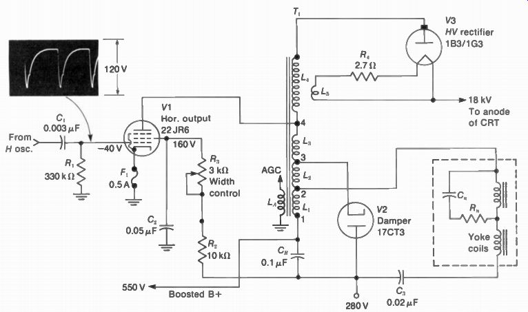
FIGURE 22-2 SCHEMATIC DIAGRAM OF HORIZONTAL OUTPUT CIRCUIT USING TUBES FOR
AMPLIFIER, DAMPER, AND HV RECTIFIER.
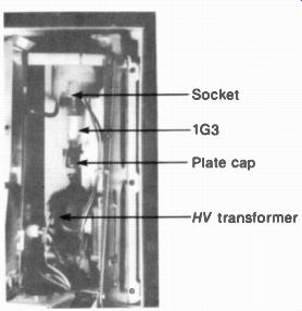
FIGURE 22-3 HV RECTIFIER AT TOP AND FLYBACK TRANSFORMER AT BOTTOM IN CAGE
ON RECEIVER CHASSIS. THE 1G3 IS MOUNTED UPSIDE DOWN.
22-2 The Horizontal Amplifier
The block diagram in Fig. 22-1 corresponds to the schematic in Fig. 22-2, using tubes in the horizontal output circuit. V1 is the amplifier, transformer coupled at terminal 2 to the deflection coils in the yoke. V2 is the diode damper. It is tapped higher at terminal 3 in order to provide more boosted B+ voltage. V3 is the high-voltage rectifier, with its filament winding L, on T. The auxiliary winding L, supplies horizontal flyback pulses for the AGC stage. The high-voltage rectifier and flyback transformer are usually in a metal cage on the receiver chassis (Fig. 22-3). Circuit components. In Fig. 22-2, C, and R, couple the sawtooth voltage from the horizontal oscillator to the output tube. The grid-driving voltage is 120 V p-p. Grid-leak bias of -40 V is developed because grid current flows when the positive peak of input voltage drives the grid positive. In fact, measuring this bias with a dc voltmeter is a good way to see if the output tube has grid drive from the oscillator. Normal dc bias means normal ac drive. With less drive, the bias is reduced. Zero bias means no drive. The output tube should not be operated without grid drive, as there is no safety bias in the cathode circuit. The 0.5-A fuse in the cathode protects the tube and transformer against excessive current.
The plate current of V1 can flow from terminal 4 on T, through L„, L2, and L, to CB, which provides boosted B+ as the source of plate supply voltage. Current in the output tube is a load on C„, making it discharge. However, C„ is recharged when the damper conducts. Note that C„ blocks direct current from the deflection coils, which would shift the horizontal centering.
The width control R3 varies the screen grid voltage on the output tube. Increasing the screen voltage-increases the width. In many circuits, the screen-grid voltage is adjusted by taps to change the series resistance, instead of by a variable control, C, is the screen-grid bypass capacitor.
It should be noted that the suppressor grid usually has a small positive bias voltage to prevent parasitic oscillations in the horizontal output tube. In addition, the control grid may have 50- to 100-ohm series resistance as a parasitic suppressor. The parasitic oscillations reduce the gain of the output tube and may produce thin, black vertical lines at either side of the raster.
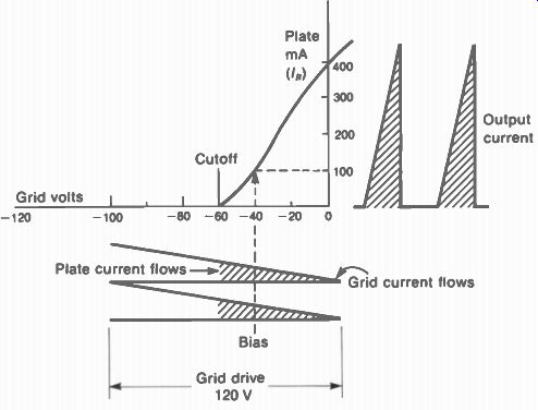
FIGURE 22-4 OPERATION OF HORIZONTAL OUTPUT TUBE SAWTOOTH PLATE CURRENT FLOWS
FOR ONLY THE PART OF THE GRID VOLTAGE INDICATED BY THE SHADED AREA
Harmonic tuning. The horizontal output trans former often has a capacitor of about 150 pF across part of the winding to resonate at an odd harmonic of 15,750 Hz. Either the third or the fifth harmonic is generally used. The harmonic component is phased to reduce the peak flyback voltage on the amplifier.
Circuit operation. As the linear rise of sawtooth input voltage drives the grid in the positive direction, the amount of plate current increases.
The result is a sawtooth rise of current in T, and the yoke coils. At the peak of the sawtooth input, the grid voltage drops sharply to a value more negative than cutoff. This negative grid drive cuts off the amplifier. As a result, V1 stops supplying current to the output circuit. The output tube remains cut off while the grid-driving voltage completes its swing in the negative direction for the flyback. Also, the tube remains cut off until the linear rise in the positive direction makes the instantaneous grid voltage less negative than the cutoff voltage. Then the saw tooth rise in grid voltage produces a sawtooth rise of current again in the output circuit to produce the next cycle of operation.
Figure 22-4 shows the grid-plate transfer characteristic curve of the horizontal output tube. The grid voltage is a sawtooth wave. How ever, the plate current flows in pulses corresponding to only part of the sawtooth voltage input. When the grid voltage due to the bias and driving voltage is more negative than cutoff, no plate current flows. For approximately two thirds of the cycle, however, the sawtooth input voltage drives the grid voltage less negative than cutoff to produce a linear rise in plate current.
This time is indicated by the shaded area of grid voltage. As an example, when the ac input voltage drives the grid voltage 30 V more positive than the bias of -40 V, the instantaneous grid voltage is -10 V, allowing plate current to flow.
The amount of grid-leak bias is approximately 90 percent of the peak positive drive.
Horizontal output tube. This is a beam-power amplifier which supplies the required amount of scanning current. As an example, the 6D05 maximum ratings are 24-W plate dissipation, 315-mA average cathode current with 1,100-mA peak value at the end of trace, and 6.5-kV peak positive pulse at the plate during flyback. Maximum dc plate supply voltage is 990 V, including boosted B+.
22-3 Damping in the Horizontal Output Circuit
The inductance of the output transformer and scanning coils, with their distributed and stray capacitances, provides a tuned output circuit that can oscillate at its resonant frequency. Oscillations occur because the flyback on each sawtooth wave of current produces a rapid change in current that generates a high value of induced voltage across the inductance. The output circuit then oscillates at its natural resonant frequency by shock excitation. This effect is called ringing.
The oscillations, at about 70 kHz in the horizontal output circuit, would continue past flyback time and produce ripples on the scanning-current waveform, as shown in Fig. 22-5a.
Since the scanning current produces deflection, the electron beam also oscillates back and forth in accordance with the oscillatory ripples.
As a result, the oscillations can produce one or more white bars at the left side of the raster, as shown in Fig. 22-5b. The bars are at the left because the oscillations occur immediately after flyback time. The bars are white because the electron beam scans these areas several times during every horizontal line traced, as the oscillations make the horizontal scanning current repeat equal amplitudes at different times.
Ringing occurs in the horizontal output circuit, primarily, rather than in vertical scanning, be cause the fast horizontal flyback produces high values of induced voltages.
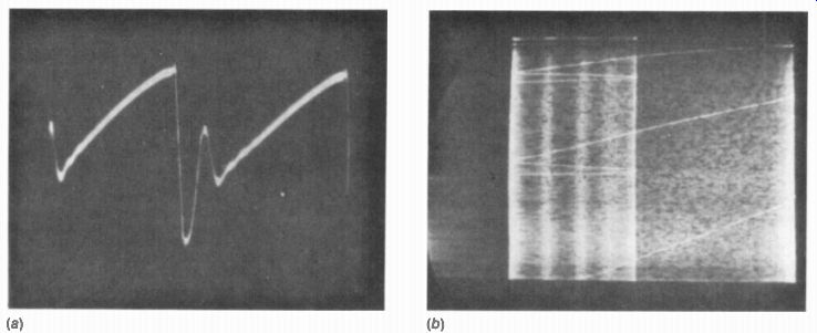
FIGURE 22-5 EFFECT OF INSUFFICIENT DAMPING IN HORIZONTAL OUTPUT CIRCUIT (a)
OSCILLATIONS IN SCANNING CURRENT (b) WHITE BARS AT LEFT SIDE OF RASTER CAUSED
BY OSCILLATIONS
FIGURE 22-6 SHOCK-EXCITING A TUNED CIRCUIT INTO OSCILLATION (a) SWITCH IS CLOSED FOR BATTERY E TO SUPPLY CURRENT AND VOLTAGE FOR L AND C (b) SWITCH IS OPENED AND SELF-INDUCED v, ACTS AS GENERATOR. (c) REVERSED POLARITIES ONE HALF CYCLE LATER WITH v, AS GENERATOR
Shock-excited oscillations. The action of shock-exciting a tuned circuit into oscillations is illustrated in Fig. 22-6. In a the switch S has been closed and current flows through L and R, while the distributed capacitance C charges to the applied voltage. When the switch is opened in b, the voltage E is disconnected from the tuned circuit. Then the change in applied voltage can make the tuned circuit start oscillating.
The tuned circuit oscillates without the battery because the energy stored in the electromagnetic field of L and the electrostatic field of C while the battery was connected provides the required current and voltage. The current in the tuned circuit and the voltage across it oscillate with decreasing amplitudes until the stored energy is dissipated in the resistance. R is the internal resistance of the coil. The switch S corresponds to the action of the deflection amplifier. It conducts during trace time to supply current to the output circuit but then is cut off at flyback time by the grid-driving voltage.
The current in the coil decays toward zero when the switch is opened. However, the sharp change as the current starts to decline produces a large self-induced voltage across L. Now the coil is a generator producing voltage that keeps the current flowing in the same direction through the inductance as when the switch was closed. This is illustrated in b of Fig. 22-6. At the same time the capacitor discharges through L and R, reducing the voltage across C. Its discharge current is in the same direction as the current in the coil.
A little later the capacitor is completely discharged and the voltage across C is zero.
The current i L produced by the coil still is in the same direction, however, charging C to produce a voltage of opposite polarity from the original battery voltage. As the current in the coil decays to zero, the voltage across C charges to its maximum value.
Then the capacitor voltage becomes the generator as it discharges to produce the current i,. through L and R, as shown in Fig. 22-6c.
This current through the coil is in the opposite direction from the original current from the battery. When the capacitor voltage is down to zero, the coil again acts as the generator to maintain the current. C then charges with its original polarity. As a result, the inductance and capacitance interchange energy, making the tuned circuit oscillate.
The waveforms of the oscillations are shown in Fig. 22-7. Notice that the current and voltage are 90° out of phase with each other, as the current is maximum when the voltage is zero. During the first half-cycle of oscillations:
1. The current reverses from maximum in one direction to maximum in the opposite direction.
2. The voltage reaches its maximum negative value and returns to zero.
The LC circuit oscillates at its resonant frequency, with reduced amplitude for successive cycles until the stored energy is dissipated in the resistance. The frequency is approximately 1 /(2 pi IC), when R is small. How long the oscillations continue depends upon the Q of the circuit. The higher the series R, the lower the Q and the sooner the oscillations decay to zero. A low value of resistance in parallel with the circuit has the same effect as a high series resistance in reducing the Q and damping the oscillations.
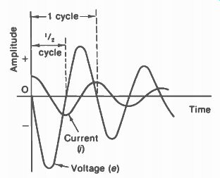
FIGURE 22-7 CURRENT AND VOLTAGE WAVEFORMS IN OSCILLATING LC CIRCUIT. NOTE
THAT i AND e ARE 9if OUT OF PHASE.
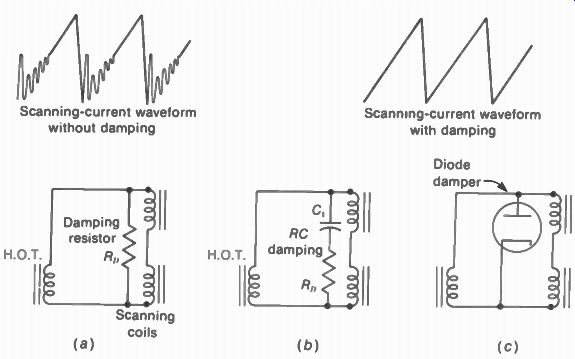
FIGURE 22-8 METHODS OF DAMPING (a) SHUNT RESISTOR; (b) RC CIRCUIT, (c) DIODE
DAMPER
Damping methods. The undesired oscillations can be eliminated from the linear rise on the sawtooth wave by connecting a damping resistance R„ in parallel with the scanning coils as shown in Fig. 22-8. Because of its low value, which is about 1,000 ohm or less, R1 , lowers the Q of the output circuit, reducing the amount of self-induced voltage. With just a simple resistance for damping, however, some of the scanning current is shunted through the parallel resistor. By the insertion of a capacitor C, in series with R,„ as in Fig. 22-8b, the scanning current can be prevented from flowing through the damping resistor while the high-frequency oscillations are damped out.
Damping with a shunt resistor is usually employed in the vertical output circuit. This method is not suitable for the horizontal output circuit, however, because there should be no damping during flyback time.
For horizontal damping, a diode damper is used, as illustrated in Fig. 22-8c. The diode can be an open circuit when it is not conducting, to allow a fast horizontal flyback. Then it con ducts to act as a low damping resistance during trace time. The first half-cycle of oscillations makes the diode plate voltage negative. This prevents conduction in the damper. Meanwhile, the current in the horizontal deflection coils drops rapidly to produce the fast horizontal flyback. After the first half-cycle of oscillations, the damper plate voltage is positive, causing conduction. Then the diode is a relatively low resistance across the horizontal deflection coils that can damp out the oscillations.
22-4 Horizontal Scanning and Damping
When the horizontal output tube conducts to supply current for the horizontal scanning coils, the linear rise in current deflects the electron beam to the right side of the raster. During this time, energy is stored in the inductance and capacitance of the output circuit. Then, when the deflection amplifier tube is cut off, the output circuit starts oscillating.
The first half-cycle of oscillations is al lowed to continue undamped for a fast flyback from the right side of the raster to the left side.
After the retrace, though, the damper conducts to make the oscillations decay to zero. The damped current in the horizontal scanning coils deflects the electron beam from the left side of the raster toward the center. Just before the damped current decays to zero, the deflection amplifier starts conducting again to finish the trace to the right edge of the raster.
The operation of the diode damper in the horizontal output circuit is illustrated in Fig. 22-9. The first half-cycle of oscillations makes the damper plate negative, as shown in Fig. 22-9a. Then the diode cannot conduct. As a result, the undamped current in the deflection coils drops sharply from its maximum value to zero and reverses to its maximum in the opposite direction very quickly for a fast flyback.
With a frequency of 70 kHz for the oscillations in the horizontal output circuit, the period of a half cycle is 1/0.14 ,us, resulting in a flyback tine of approximately 7 /us. This half-cycle is from maximum positive i to maximum negative i for the waveforms in Fig. 22-10.
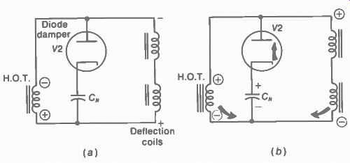
FIGURE 22-9 DAMPER DIODE OFF G AND ON. (a) PLATE NEGATIVE TO PREVENT CONDUCTION
DURING RE-TRACE. (b) PLATE POSITIVE FOR CONDUCTION AT START OF TRACE.
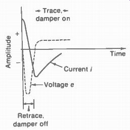
FIGURE 22-10 WAVEFORMS OF VOLTAGE e AND CURRENT i FOR HORIZONTAL DEFLECTION
COILS WHILE OUTPUT TUBE IS CUT OFF
The voltage across the oscillating circuit is 90 out of phase with the current, as shown in Fig. 22-10. Therefore, the polarity of damper plate voltage reverses to become positive just as the current starts to decrease from its maximum negative value. This is the time for the start of the trace. Now the damper conducts because of positive plate voltage.
Conduction in the diode is illustrated in Fig. 22-9b. Note that C„ is charged by the damper current at this time. As the damped current declines to zero, the electron beam is deflected from the left side of the raster toward the center.
Finally, the voltage across C„ biases the diode damper out of conduction. With zero current in the scanning coils, the electron beam would be undeflected at the center. Before the damped current declines to zero, however, the output tube starts conducting. Its linear rise of current then completes the trace to the right side of the raster.
Figure 22-11 illustrates how the current supplied by the deflection amplifier and the damped current in the output circuit combine.
The result is sawtooth current in the deflection coils for the full horizontal trace from left to right across the scanning raster. Note that both components of the scanning current for the trace deflect the electron beam toward the right. The decrease in damped current of negative polarity varies in the same direction as the positive rise of current produced by the output tube.
In summary, the horizontal scanning occurs in three steps:
1. The output stage supplies current for the horizontal scanning coils to deflect the electron beam to the right edge of the raster.
2. The undamped oscillation in the horizontal output circuit, while the output stage and damper are not conducting, produces the rapid reversal of scanning current required for the fast flyback from right to left.
3. Immediately after the flyback, the damper conducts while the output stage is cut off, to provide the reaction scanning current for the trace at the left side.
The damper tube must withstand the high negative voltage pulse at the plate, have good cathode-to-heater insulation because of the 6+ boost voltage at the cathode, and be able to con duct the peak values of scanning current. Typical maximum ratings for the 6CL3 half-wave rectifier as a diode damper are 5.5-kV peak inverse plate voltage, 1,300-mA peak plate current, --900-V average cathode-heater voltage, and 8.5-W plate dissipation.
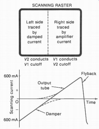
FIGURE 22-11 HOW THE DAMPED CURRENT AND OUTPUT CURRENT COMBINE TO PRODUCE
HORIZONTAL SCANNING IN THE RASTER.
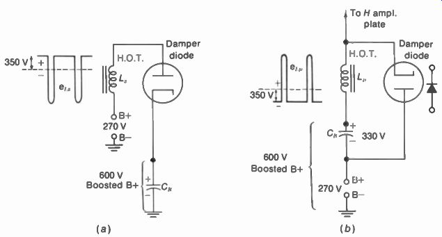
FIGURE 22-12 PRODUCING THE BOOSTED B+ VOLTAGE. EITHER A TUBE OR A SILICON
DIODE CAN BE USED. (a) DAMPER IN SECONDARY TO RECTIFY POSITIVE POLARITY OF
THE AC DEFLECTION VOLTAGE (b) INVERTED DIODE IN PRIMARY TO RECTIFY NEGATIVE
POLARITY OF THE AC DEFLECTION VOLTAGE
22-5 Boosted B+ Voltage
The damper diode is a half-wave rectifier for the ac deflection voltage produced during trace time in the horizontal output circuit. Its do output voltage then is added to the B+ supply voltage. The sum of the two voltages is boosted B+. Damper in secondary. In Fig. 22-12a, 270 V is applied to the low end of L . _p while the other side is connected to the damper plate. Therefore, when the damper conducts, it charges C„ in the cathode circuit to the B+ voltage. The path of charging current is through L, and from cathode to plate in the damper, charging CB to 270 V with the cathode side positive.
In addition, however, the ac deflection voltage e _ps, which produces sawtooth current in the scanning coils, makes the diode plate 350 V more positive during horizontal trace time As a result, CB charges to a voltage about 330 V higher than 270 V, or to 600 V. The path of charging current is the same as when the B supply charges CB. In effect, the ac deflection voltage is in series with the B supply voltage and the damper tube to produce the boosted B+ voltage across CB. The damper circuit in Fig. 22-12a is for an output transformer with an isolated secondary, which can have the polarity of deflection shown with negative flyback pulses. In an autotransformer, however, any part of the winding must have deflection voltage with positive flyback pulses. This is the same polarity as the primary winding. Then the damper circuit with an inverted diode, shown in Fig. 22-12b, is used.
Damper in primary. In Fig. 22-12b, the diode is inverted. Then the ac input voltage is applied to the cathode. This connection is necessary because the deflection voltage is negative in the primary during trace time. The negative polarity of ac deflection voltage at the cathode produces plate current in the diode to charge CB. Note that the rectifier plate current still charges GB with its cathode side positive. CB is in series with the B supply voltage. The potential difference between the positive side of CB and chassis ground, therefore, is 600 V. Note that in both a and b of Fig. 22-12, the damper plate or anode must have a dc connection to the B+ supply.
The damper in the primary is the circuit generally used. Tubes now have the voltage rating to prevent arcing between cathode and heater, while semiconductor diodes do not have a heater.
Uses for boosted B+. This voltage is commonly used for the horizontal output tube, horizontal oscillator, vertical oscillator, and vertical amplifier. The higher plate supply voltage allows more power output with improved linearity. In addition, the screen-grid supply of the picture tube is generally boosted B+ voltage. It is important to note that the B+ boost circuit must be operating in order to produce normal plate voltage for all these stages.
A question often asked is, "How can the horizontal amplifier operate when the receiver is first turned on, before boosted B+ voltage is available across CB?" In effect, this is a "boot strap circuit," where the output stage increases its own plate supply voltage. Notice in Fig. 22-12 that for the circuits in both a and b the amplifier plate circuit can return to B+ through the cathode-to-plate path in the conducting damper tube. Therefore, the horizontal output tube starts conducting with just B+ voltage for the plate supply. After a few cycles of operation, boosted B+ voltage is available across CB.
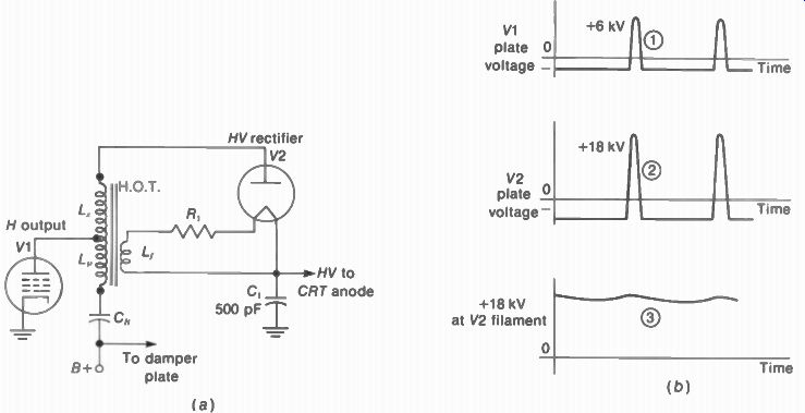
FIGURE 22-13 PRODUCING THE FLYBACK HIGH VOLTAGE. EITHER A TUBE OR A SILICON
DIODE CAN BE USED FOR THE RECTIFIER. (a) TYPICAL CIRCUIT: (b) VOLTAGE WAVE
SHAPES WITH NUMBERS FOR THE STEPS EXPLAINED IN TEXT.
22-6 Flyback High Voltage
The voltage pulse produced in the horizontal output circuit during the first half-cycle of oscillations for flyback provides the dc high voltage required for the CRT anode. As illustrated in Fig. 22-13, operation of the flyback high-voltage supply can be summarized as follows:
1. The flyback pulse has positive polarity at the plate of the horizontal amplifier in the primary of the output transformer, as shown by waveshape 1. Both the damper and amplifier tubes are cut off for the retrace. The first half-cycle of undamped oscillations produces the high-voltage flyback pulse. A typical value is 6,000 V at the amplifier plate.
2. The high-voltage winding L, steps up the flyback pulse for the plate of the high-voltage rectifier V2, as shown by waveshape 2.
This amplitude is 18 kV because of the 3:1 voltage stepup.
3. With the stepped-up ac deflection voltage at its plate, V2 conducts to produce positive dc output voltage at the cathode. This voltage is filtered to provide the steady dc output shown by waveshape 3. The dc output voltage is approximately equal to the peak positive ac input of 18 kV. When the high-voltage rectifier conducts, current can flow from cathode to plate in V2, through L, and L _p in the output transformer, discharging C„ slightly and charging the filter C. This is usually the anode capacitance of the picture tube. Since the ripple frequency is 15,750 Hz for the half-wave rectifier, 2,000 pF is enough capacitance to provide the required filtering. 13,1 is a voltage-dropping resistor for the heater of V3. Its heater power is supplied by L f, which is a single-turn loop on the transformer core.
The amount of high voltage is maximum when the brightness is at a minimum. The reason is that there is less load current on the high-voltage rectifier. It is important to note that with a flyback high-voltage supply, the dc output for anode voltage cannot be produced without the ac deflection voltage input to the plate of the high-voltage rectifier. Therefore, the horizontal deflection circuits must be operating to have brightness on the screen of the picture tube.
22-7 Horizontal Deflection Controls
The only adjustments usually are for width and linearity. However, even these may be omitted in some receivers. The reason is that incorrect adjustments can cause too much average dc plate current in the horizontal output stage.
Width control. Varying the screen-grid voltage of the output tube, as in Fig. 22-2, is a common method. Instead of the variable resistance, though, variable taps on a voltage divider can be used. Another method uses a width coil in parallel with part of the secondary winding of the output transformer. A typical coil is shown in Fig. 22-14.
FIGURE 22-14 COIL FOR WIDTH OR LINEARITY CONTROL. L IS 2 TO 18 mH. R IS 14 U.
Efficiency coil. L, in Fig. 22-15 forms a parallel resonant circuit with C„ and C _p tuned to 15,750 Hz approximately. Adjusting L, shifts the phase of the 15,750-Hz ripple in B+ boost voltage for the horizontal amplifier. The parallel resonance allows minimum average dc plate current in the output tube. This is the condition for maximum efficiency. The efficiency coil L, is generally adjusted for minimum cathode current on the horizontal output tube. Some receivers provide connections for inserting a dc milliammeter in the cathode circuit.
In addition, L, affects the voltage at the transition period when the damper finishes conduction and the amplifier starts. Therefore, L, adjusts linearity at the center of the raster. The main requirement, however, is minimum cathode current in the output tube for maximum efficiency.
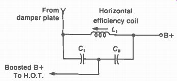
FIGURE 22-15 CIRCUIT FOR HORIZONTAL EFFICIENCY COIL WITH L OF 1 TO 8 mH.
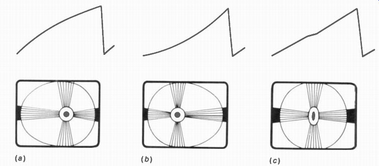
FIGURE 22-16 NONLINEAR HORIZONTAL SCANNING. (a) STRETCHING AT LEFT AND CROWDING
AT RIGHT, (b) REVERSE EFFECT, (c) CROWDING AT CENTER.
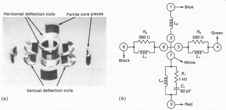
FIGURE 22-17 A Kr YOKE FOR MONOCHROME PICTUE TUBE. DIAMETER, 3 IN. (a) CUT
AWAY VIEW, (b) WIRING DIAGRAM.
Horizontal linearity. Three examples of non-linear horizontal scanning are illustrated in Fig. 22-16. To relate the current waveshapes to the scanning, remember that:
1. Damped current produces the left side of the trace.
2. The beam is at the center with zero current, when the damped current approaches zero and the output stage starts to conduct.
3. Plate current of the output stage completes the trace at the right side.
How fast the damped current decays to zero depends on the damper tube and B+ boost capacitor. The time when the output tube starts to conduct depends on its grid-leak bias and plate voltage. Conduction is delayed until the driving voltage is positive enough to make the instantaneous grid voltage less than cutoff. How far the beam is deflected to the right edge depends on the peak plate current in the output stage.
In Fig. 22-16a, the picture information is stretched at the left and crowded at the right.
With people in the picture, they look too broad at the left or too thin at the right. This type of nonlinearity can be caused by too much horizontal drive and too little inductance in the width coil. A weak horizontal output tube produces the same nonlinearity, but with reduced width.
The reverse happens for the nonlinear scanning in Fig. 22-16b, where the left side is crowded and the right side stretched. This effect can be caused by a weak damper tube or too much load current for C„. With either type of nonlinear horizontal scanning, a person at the center of the screen appears to have one shoulder broader than the other.
Figure 22-16c illustrates crowding at the center. This can be caused by damper current decaying to zero before the output tube starts to conduct.
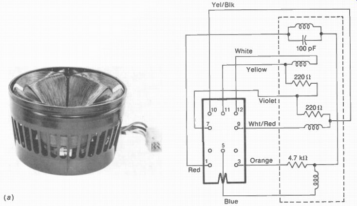
FIGURE 22-18 A 90 YOKE FOR COLOR PICTURE TUBE. (a) PHOTO. DIAMETER IS 6'/,
IN (b) WIRING DIAGRAM (TRIAD-UTRAD)
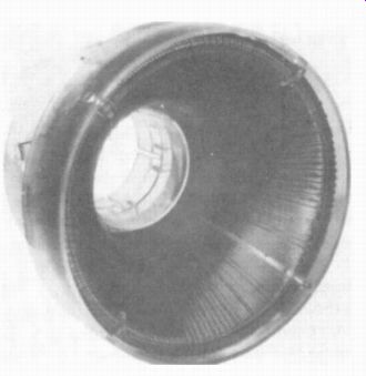
FIGURE 22-19 TOROIDAL YOKE. FOR 90 DEFLECTION ANGLE. DIAMETER IS 4 IN. (GTE
SYLVANIA INC.)
22-8 Deflection Yokes
Since the current in the scanning coils deflects the electron beam, the yoke is rated in terms of deflection angle. Typical values are 70 °, 90 to 92°, and 110 to 114°. Monochrome yoke. See Fig. 22-17. Typical values for a 90 degr yoke may be L„ of 12 to 30 mH with R of 25 12 in the horizontal scanning coils. For the vertical coils, L, is about 42 mH with R of 40 Ohm. It should be noted that a 1100 yoke would be about 1 in. shorter, with a smaller opening for the narrow neck on the picture tube. The construction in Fig. 22-17a shows why this type is called a saddle yoke.
In the wiring diagram in Fig. 22-17b, R, and R„ are damping resistors in parallel with the vertical coils. R, and C, form an anti-ringing network across one horizontal coil. Without the proper values for balancing capacitances, the horizontal ringing produces thin, white vertical lines at the left side of the raster. All these components are inside the yoke housing.
Color yoke. See Fig. 22-18. This is a 90° yoke for color picture tubes. The characteristics are L„ of 12 mH with R of 911 for the horizontal coils, and L, of 24 mH with R of 13 I/ for the vertical coils. The yoke diameter is 6 1/2 in., length 3 3/8 in., and weight 31/4 lb. Although it is larger than the yoke in Fig. 22-17, it also uses the saddle construction for the deflection coils.
Toroidal yoke. A toroid is an inductance wound in a closed loop to concentrate the magnetic field. It can be constructed for either a 90 ° or a 110° deflection angle. The 90° yoke in Fig. 22-19 is made to mount directly on the neck of the color picture tube. This yoke has an extra winding for dynamic convergence. The horizontal coils have L„ of 1 mH series-connected, but they can be in parallel for L„ of 0.5 mH. The vertical coils have L, of 2 mH in series. The dc resistance of the coils is only 1 to 2 11. The relatively low impedance, compared with saddle yokes, makes the toroidal yokes suitable for deflection circuits using transistors or thyristors.
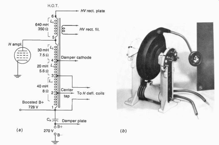
FIGURE 22-20 FLYBACK TRANSFORMER FOR MONOCHROME RECEIVER OF AUTOTRANSFORMER,
(b) PHOTO. (TRIAD- UTRAD) (a) SCHEMATIC
22-9 Horizontal Output Transformers
Typical units for the H.O.T. or flyback transformer are shown in Figs. 22-20 and 22-21.
Autotransformer windings. In Fig. 22-20a, the total winding between 1 and 5 is the primary L _p for plate current of the amplifier. This includes L 2. L _p and L. The tapped winding between 3 and 1 is the secondary L , to step down the voltage for the deflection coils. Note that the turns ratio is between all the turns in L I , and the number of turns tapped for L . Since there is no isolated secondary winding for polarity inversion, all the taps on an autotransformer have voltage of the same polarity as the plate voltage on the amplifier. In Fig. 22-20a, for instance, the voltage at terminal 3, 4, or 5 has a rectangular waveshape with positive flyback pulses. The drop in plate current for retrace induces voltage of positive polarity across the inductance.
The positive flyback pulses require that the damper diode be inverted. These connections are shown in Fig. 22-12b for flyback pulses to drive the damper cathode positive. This corresponds to negative anode voltage to prevent the damper from conducting during flyback.
With an autotransformer, the damper can be tapped up on the winding for a higher boosted B+ voltage. As shown in Fig. 22-20a, the tap at 4 for the damper has more deflection voltage than the tap at 3 for the scanning coils.
As a result, the damper charges CB to a higher voltage. Some receivers have an extra diode to rectify more deflection voltage that is added in series with CB. This output is called boosted boost voltage. It can be as high as 1,100 V. The winding L„ at the top of Fig. 22-20a steps up the primary voltage to supply ac input to the high-voltage rectifier. For a tube, its filament power is also taken from the output transformer. Positive flyback pulses of about 6 kV at the amplifier plate can be stepped up to 18 kV. The amount of stepup is limited by the fact that increased L and stray C reduce the resonant frequency of the output circuit. 1„, is a separate winding with many turns of fine wire, which is the reason for its relatively high R of 350 to 790 11. This winding is in series with L _p on the auto transformer. For color receivers, the high-voltage supply generally includes a focus rectifier also, as shown in Fig. 22-21.
Auxiliary windings. Although they are not shown in Fig. 22-20, the horizontal output trans former usually has connections that provide flyback pulses for auxiliary functions in the receiver. These connections may be taps on the autotransformer or isolated windings. Typical functions include keying pulses for the AGC stage, sample of the scanning frequency for horizontal AFC, and horizontal retrace blanking for the video amplifier or picture tube. Color receivers also need the horizontal flyback pulses to key on the burst separator. In addition, the horizontal output is used for pincushion correction and dynamic convergence circuits.
FIGURE 22-21 FLYBACK TRANSFORMER FOR COLOR RECEIVER NOTE NUMBERED TERMINALS FOR TAPS. (TRIAD-UTRAD) --- H centering Focus control
Focus rectifier
22-10 Analysis of Horizontal Output Circuit
The inductance values in Fig. 22-20a can be used for some approximate calculations to illustrate more details of how the horizontal output circuit functions. Unity coupling between windings is assumed because of the powdered-iron or ferrite core. Also, the coil resistances can be neglected, as the induced voltages are much greater than the IR drops.
In analyzing the inductance values, we can start with the secondary winding L s for the deflection coils, as they require a specified amount of current for full deflection. The secondary inductance here is made 40 mH to be twice the total inductance of 20-mH deflection coils connected across L,. Higher values of L s allow more inductance in the primary for a given turns ratio. However, too much inductance can make the flyback time too long. The value of 20 mH, then, is suitable for L. In the primary, the inductance L _p for the autotransformer includes all the turns of L 2, L _p and L. The total primary inductance L, then is 90 mH, equal to 30 mH for L, plus 20 mH for L, plus 40 mH for L. The turns ratio for voltage stepup to L _p from L, is equal to the square root of their inductance ratio, or 0 0/ i„. The square root is based on the fact that inductance of a coil in creases as the square of its turns. This ratio of V91/ 41> equals V2.25, which is 1.5 for the turns ratio of L i , to L s. With one and one-half the number of turns for L,„ its voltage is 50 percent more than the voltage across L s.
In order to calculate the induced voltages we can assume a flyback of 8 As. This time corresponds to one-half cycle of undamped oscillations at 62.5 kHz. Trace time equals 8 As subtracted from the line period of 63.5 As. Then the remainder of time for trace is 55.5 u-s.
Let the peak-to-peak yoke current be 1,200 mA in the 20-mH horizontal deflection coils. This value is derived from 400-mA peak plate current in the output tube stepped up to 600 mA in the yoke by the turns ratio. The opposite peak of 600 mA is a result of oscillation in the output circuit after the amplifier cuts off.
During trace, the rate of change of current in the yoke is 1,200 mA during 55.5 As. However, for flyback the rate of change is 1,200 mA in 8 As.
These values are necessary to calculate the induced voltages as equal to L di/dt.
The voltages induced by the rise of current during trace are negative with respect to chassis ground at all terminals on the autotransformer. During flyback, the fast drop of current induces positive voltages of much higher amplitude. These voltages are shown in Fig. 22-22.
Induced voltages during retrace. The flyback voltage induced across the yoke coils by a 1,200-mA change in 8 u-s is
+e„ = LcIL
• dt
' 2 1 00 x 10 " = 20 x 10-3 x 8 x 10 "
+e„ = 3,000 V
This voltage is also across L. Since the turns ratio of L _p to L, is 1.5:1, the voltage across L _p is stepped up by 1.5 to be 4,500 V at the plate of the output tube.
The high-voltage winding L„ develops 4 x 3,000 = 12,000 V during flyback. This voltage is four times the secondary voltage because L„ is sixteen times greater than L. The 12,000 V across L„ is in series with the 4,500-V flyback pulse across L i . to provide 16,500-V peak positive ac input to the plate of the high-voltage rectifier.
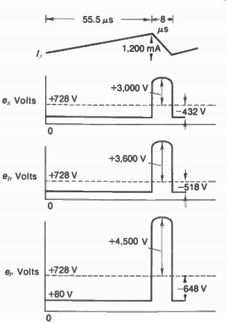
FIGURE 22-22 INDUCED VOLTAGES PRODUCED BY YOKE CURRENT, CALCULATED FOR THE
TRANSFORMER IN FIG. 22-20a
Induced voltages during trace. These are much smaller because of the slower rate of change of current. Also, the increasing current induces negative voltage. The amount of voltage induced across the yoke coils by a 1,200-mA change in 55.5 As is di
- = L- dt
[...]
Notice that the damper cathode at terminal 4 is tapped higher than L. This connection results in more boosted B+ voltage, as more deflection voltage is applied to the damper for rectification. The combined turns of L, and L, provide a voltage stepup of approximately 1.2 with respect to L. Therefore, the damper voltage e _p is 20 percent more than e_. Then e_ equals 518 V. This much voltage is available to drive the damper cathode negative for diode current to charge CH. Note that the 518 V across C„ is for the boost only. In addition. C„ is in series with the B of 270 V. Therefore, the boosted voltage at terminal 1 with respect to chassis ground would be 270 4 518 - 788 V. With a typical load of 10 mA average current on the boost supply, however. its dc voltage is a little less than the peak ac input. In this example, the boost voltage alone is 458 V. This value added to the B - of 270 V provides the 728-V average axis shown in Fig. 22-20. Then 728 V is the amount of boosted B+ voltage available from terminal 1 at the low end of the autotransformer.
22-11 Complete Horizontal Deflection Circuit
As shown in Fig. 22-23 for a monochrome receiver with tubes, the stages included are the horizontal oscillator with its AFC, the output amplifier, the damper, and the high-voltage rectifier. A transistorized circuit is shown in Fig. 22-28. A horizontal output circuit using silicon controlled rectifiers is shown in Fig. 22-29. Integrated circuit (IC) units are not used for deflection because of the high power requirements.
In Fig. 22-23, the horizontal oscillator V1 is a cathode-coupled multivibrator driving the deflection amplifier V2 with autotransformer coupling to the horizontal deflection coils in the yoke. The damper V3 is an inverted diode rectifier producing boosted voltage of 660 V. The high-voltage rectifier V4 supplies 18 kV for the picture tube, with its anode capacitance as the high-voltage filter. Note that the octal yoke plug has a jumper between pins 1 and 8, which closes the 6- return to chassis ground for operation oz the power supply. Removing the yoke plug makes the entire receiver dead, therefore, be cause the B-supply circuit is open.
The oscillator is locked in sync by dc control voltage from a sync discriminator connected to grid pin 2. In the plate circuit, R _p, is tie load resistor in series with the sine-wave stabilizing circuit consisting of L„„ and C4 „ 2 The voltage peak across the common-cathode resistor R _p7 cats off this triode section. Plate voltage output is coupled by C,„ to the opposite triode section, which serves as a discharge tube. Its grid resistance is varied by the hold control to adjust the free frequency of the oscillator. Plate pin 6 connects to B+ through R,„„. The sawtooth capacitor is C157 . Note the peaking resistor R„ to provide trapezoidal grid voltage for driving the output tube. The peaking resistor can be on either side of the sawtooth capacitor, as they are in series. C,„„ is the coupling capacitor, with grid resistor R„. The series grid resistor R„„ limits the peak grid current charging the coupling capacitor for grid-leak bias, in order to reduce radiation of horizontal pulses.
The grid-leak bias of -40 V on the output tube is produced by drive from the horizontal oscillator. There is no cathode bias. Screen-grid voltage is obtained from the B+ line, with R„, the screen-dropping resistor and C,„„ its bypass.
The boosted B-4- of 660 V is used for the plate of the output tube, the vertical deflection circuit, through the isolating resistor R 1,;7, and for the screen grid of the picture tube.
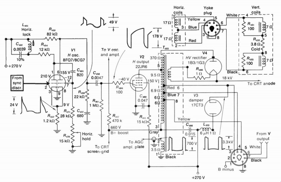
Fig. 22-23
In the plate circuit of the output tube, the top winding of the autotransformer T,„; , supplies positive flyback pulses for the plate of the high voltage rectifier. The primary winding for the amplifier plate consists of all turns between terminals 5 and 3. Note that terminal 3 at the low end is the source of boosted B+ voltage of 660 V. C466 is the boost capacitor. It is in series with terminal 3 and B+ connected to the damper plate. The damper cathode is tapped at terminal 6. This negative voltage during trace makes the damper diode conduct to charge C.,„„. The 6-tH choke L„„, prevents radiation of horizontal pulses by the peak damper current.
Terminals 6, 7, and 8 on the autotransformer connect to the horizontal coils in the yoke, through pins 3, 4, and 5 on the yoke plug.
Pin 4 is a center-tap connection. In this circuit, the ac deflection voltage for boost is higher than the yoke voltage by the amount of voltage across terminals 8 and 3 on the transformer. Finally, the extra winding at the bottom of T„ _p supplies positive flyback pulses for the plate of the keyed AGC stage. A separate winding is necessary so that one end can be grounded.
All waveshapes in the horizontal circuits are obtained with the oscilloscope internal sweep at 15,750/2 Hz. Although not shown here, the positive flyback pulses at the plate of the output tube can be observed by clipping the oscilloscope input cable to the insulation of the wire to the plate.
22-12 Protective Bias on Horizontal Output Tube
When the horizontal oscillator stops for any reason, there is no drive at the grid of the output tube. Its grid bias then drops to zero. Assuming no cathode bias, the tube conducts maximum plate current. The plate usually turns cherry red.
If this continues, the output tube will be burned out. To prevent this problem, the circuit in Fig. 22-24 provides protective bias on the horizontal output tube when the drive fails.
Normally, the drive will produce about -50 to -70 V grid-leak bias. This voltage makes A at the D2 anode more negative than 8 at its cathode. Then D2 is reverse-biased and cannot conduct. D2 locks out the protective bias, therefore, as long as the output tube has normal drive voltage from the oscillator.
FIGURE 22-24 PROTECTIVE BIAS CIRCUIT FOR HORIZONTAL OUTPUT TUBE.
In addition, the ac line voltage is rectified by D1 to charge C, to approximately -160 V. This rectified voltage is negative at the D1 anode. The -160 V is divided by R, and R2, which return to +700 V. As a result, point B at the D2 cathode is about -45 V. Then D2 is reverse-biased because its cathode voltage from D1 is less negative than the negative anode voltage from the grid-leak bias.
When the horizontal drive signal is lost, however, there is no grid-leak bias to make the D2 anode negative. D2 then can conduct. In effect, the conducting diode connects the negative voltage at B to the grid of the output tube.
As a result, the plate current is limited by the protective bias.
The grid will receive more than the normal -45 V at point B because the 700 V from the boost supply drops. When horizontal drive is lost, boost voltage is no longer developed by the damper. Without the positive boost voltage, point B goes even more negative and the output tube's plate current is actually cut off.
In troubleshooting the horizontal circuits, it may be necessary to disable the protective bias circuit. The easiest way to do this is to short point B to ground temporarily with a clip lead.
However, you then have to be careful not to let the output tube be damaged by the absence of horizontal drive. If the plate turns cherry red, shut off the power.
22-13 Transistorized Horizontal Deflection
When a transistor is used for the horizontal amplifier, its function is equivalent to that of an on-off switch. When the stage conducts, its very low resistance makes the horizontal output circuit essentially a pure inductance. For sawtooth current the only requirement is a steady applied voltage that is periodically cut off.
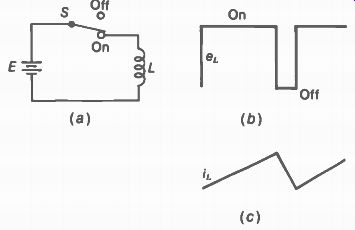
FIGURE 22-25 PRODUCING SAWTOOTH CURRENT IN INDUCTANCE L. (a) BATTERY E WITH
SWITCH S: (b) EQUIVA LENT RECTANGULAR VOLTAGE (c) SAWTOOTH CURRENT.
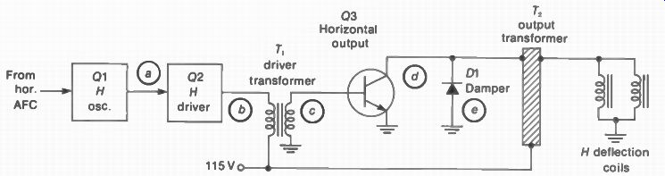
FIGURE 22-26 BLOCK DIAGRAM OF HORIZONTAL DEFLECTION CIRCUIT WITH TRANSISTORS.
LETTERS IN BALLOONS ARE FOR WAVESHAPES IN FIG. 22-27.
Sawtooth current in L. In Fig. 22-25a the battery supplies the steady voltage E through the closed switch S to the inductance L. Then S is opened to disconnect E. The equivalent result in Fig. 22-25b is the rectangular voltage e,. applied to the inductance. While E is applied, the current i 1 in the inductance rises as shown in Fig. 22-25c. The current cannot rise instantly with E because inductance produces a self-induced voltage that opposes the change in i,. For the retrace part of the sawtooth, i, drops when e t is turned off. The trace part of the sawtooth is produced while the output stage is conducting, or on. The retrace part occurs while the output stage is cut off.
Power transistors. The required power rating for the horizontal output stage is 25 to 50 W. Its resistance when conducting maximum current is 1 12 or less.
The horizontal output transistor is generally cut off for a longer period than retrace time, for better efficiency. The damper diode produces part of the trace at the left. Actually, the cutoff time of the output stage is critical. The reason is that a small increase in conduction angle can raise the average /, to a level exceeding the power rating for collector dissipation.
Typical horizontal circuit with transistors. The block diagram in Fig. 22-26 illustrates the oscillator, driver, and output stages. The driver Q2 has several functions. It is a buffer or isolation stage to prevent the output circuit from changing the oscillator frequency. With the interstage transformer T _p the voltage drive is stepped down to match the low impedance of the power amplifier Q3. In addition, the D2 circuit can be used to shape the driving voltage for the output stage. It is often necessary to stretch the cutoff time of Q3 for maximum efficiency. In the output circuit, note that the deflection coils are in parallel, for a lower impedance than with series connections.
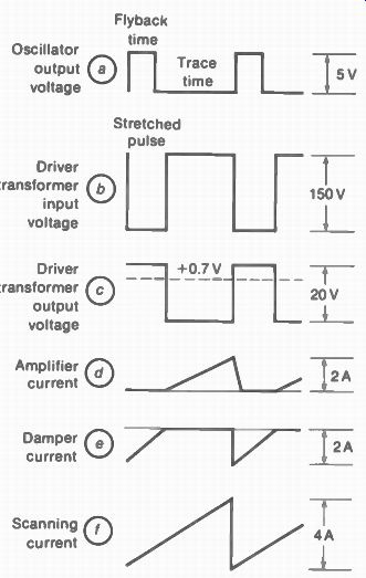
FIGURE 22-27 WAVESHAPES FOR HORIZONTAL Deflection CIRCUIT IN FIG. 22-26.
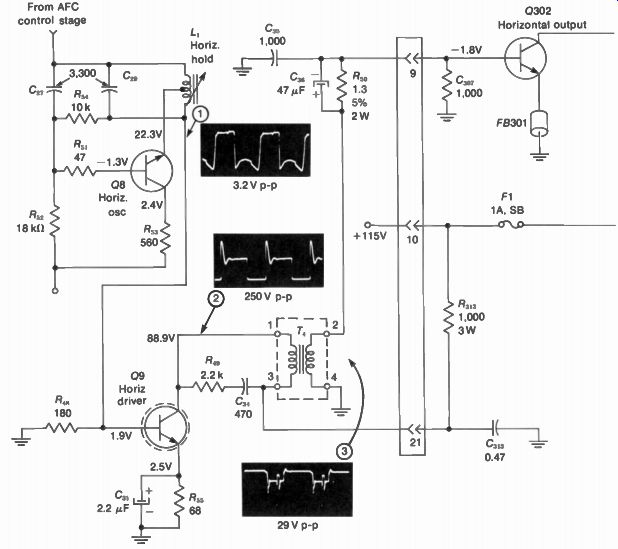
FIGURE 22-28 TRANSISTORIZED HORIZONTAL DEFLECTION CIRCUIT FOR COLOR RECEIVER.
R IN OHMS, C VALUES MORE THAN 1 IN pF. ( FROM MAGNAVOX CHASSIS T 979)
Transistor waveshapes for horizontal deflection. The waveforms in Fig. 22-27 match the numbered balloons in Fig. 22-26. The oscillator output voltage is shown in a. Note that the oscillator pulse is for flyback time, which eventually cuts off the output stage. This oscillator pulse is amplified and inverted by the driver.
The stretching of the flyback pulse is accomplished by RC networks in the driver circuit and by the interstage transformer T,.
The primary voltage in b is stepped down so that the voltage waveform in c can drive the base of the output transistor. The amplifier current in d shows that Q3 is cut off for retrace plus one-quarter of the trace at the left side of the raster. The damper Q1 fills in the missing component for trace, as shown in e. The combined result in f is sawtooth current in the yoke for the complete trace from left to right.
Typical circuit. Refer to Fig. 22-28. The horizontal oscillator Q8 supplies pulses that are amplified by the driver 09, transformer-coupled to the amplifier Q302. These stages correspond to Q1, Q2, and Q3 in Fig. 22-26. Note the oscilloscope waveshapes shown at 1 for oscillator output, at 2 for driver output, and at 3 for drive to the base of the output stage.
08 is a sine-wave oscillator using the Hartley circuit with a tapped coil in the emitter leg. The oscillator output is directly coupled to the base of driver Q9. In its collector circuit, the driver transformer T, couples the pulses to the base of the output transistor Q302. Finally, Q302 is coupled to the yoke coils by the horizontal output transformer T„,2.
The diode D301 is connected across Q302 in the polarity that allows damper current for the left side of trace when the output transistor Q302 is still cut off. Ferrite beads FB301 and FB302 are equivalent to small rf chokes to suppress parasitic oscillations.
The circuit in Fig. 22-28 is from a color receiver. Therefore, another function of the horizontal output is to provide 5-kV focus voltage, in addition to the 25.5-kV anode supply. Also, correction voltages are coupled to the convergence board and the pincushion circuits. Finally, the horizontal flyback pulses are used for blanking, horizontal AFC, and the AGC circuits.
22-14 SCR Horizontal Output Circuit
A silicon-controlled rectifier (SCR) has anode, cathode, and a gate electrode. Positive voltage at the gate turns on the anode current, with positive anode voltage. The SCR then is a closed switch. However, the gate cannot turn off the anode current. Only when the anode voltage drops too low does the SCR open. Then gate voltage can turn on the SCR again.
In Fig. 22-29 two SCR units are used for the horizontal output circuit. SCR, conducts for the trace and SCR,. for the retrace. Switching on the retrace is called the commutating operation.
Each SCR has a damper diode with in verse parallel connections. The purpose is to allow current in both directions from cathode to anode in either the SCR or its diode, depending on which anode is positive. When the diode conducts, its low resistance drops the SCR anode voltage to the cutoff level.
During horizontal trace time, SCR, is on and SCR, is off. Then the pulses from the horizontal oscillator at 15,750 Hz turn on the retrace SCR. The conduction in SCR, then cuts off the trace SCR. For troubleshooting, note that the retrace section has a dc connection to the 160-V supply through T, and the circuit breaker. It will trip open with a short in SCR, or D,.. The trace section has no dc connection to the B+ voltage. A short in SCR, or DT, therefore, will not open the circuit breaker. In both cases, though, the result will be no horizontal output and no brightness.
The test points TP1 and TP2 at each SCR anode can be used to check the resistance of the SCR with its reverse diode. Normal resistance is 1,000 ohm or higher. The positive ohmmeter lead is at the test point. A low resistance means either the diode or the SCR is shorted.
Since the SCR needs an inverse diode for this circuit, units are made with both on a common chip. The result is an integrated thyristor and rectifier (ITR).
22-15 High-Voltage Limit Control
One of the special safety features that must be incorporated in color TV receivers is a means of preventing danger from excessive x-radiation.
Manufacturers are required to incorporate some circuit that will make the picture un-viewable if the high voltage exceeds specifications.
Several different methods have been employed to meet this requirement. When the high voltage exceeds a predetermined level, some sets will blank the video, while others will cause a loss of sync. In the example of Fig. 22-30, the SCR limit switch disables the horizontal sweep, causing a complete loss of high voltage and no brightness. Not only does this make the picture un-viewable, it removes the cause of the potential radiation.
In Fig. 22-30, a positive pulse from the horizontal output transformer is rectified by CR210 to charge C _p„. During the time the pulse is applied, CR210 is biased on and C„,„ charges rapidly through the low resistance of the diode.
Between pulses, C„„ discharges slowly through the high resistance of R„„ _p equal to 1.8 M-O. With normal high-voltage levels, the average charge on C241: is not high enough to ionize the neon bulb PL1.
If the high voltage exceeds a preset value, however, the increased flyback pulse will charge C2 16 to a higher voltage. Then the neon bulb is ionized on. This causes a pulse of current to flow through F?: _p„ and The voltage drop across R„,„ makes the gate of Q209 positive.
Since the SCR already has a positive voltage applied to its anode from the horizontal module, the positive gate voltage will cause the SCR to conduct. Then it short-circuits the monsoonal sweep circuit, removing the high voltage completely. The SCR serves as a limit switch, therefore, normally open but closed to disable the horizontal scanning if there is too much high voltage.
Sometimes an arc in the picture tube or elsewhere in the chassis will trigger the SCR. In that case, it is only necessary to turn the set off for 10 s to discharge C„„ and reset the limit switch.
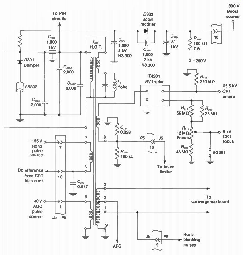
FIGURE 22-29 HORIZONTAL OUTPUT CIRCUIT USING SILICON-CONTROLLED RECTIFIERS
(SCRs), SIMPLIFIED TO SHOW SEPARATE TRACE AND RETRACE SECTIONS. D, and D,
ARE DAMPER DIODES. (RCA)
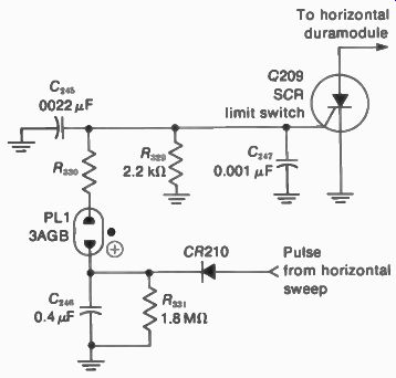
FIGURE 22-30 SCR AS LIMIT SWITCH TO DISABLE HORIZONTAL SCANNING WITH EXCESSIVE
HIGH VOLTAGE (FROM ZENITH CHASSIS 250057)
22-16 Troubles in the Horizontal Deflection Circuits
These circuits cause troubles in the width of the raster. In addition, there is no high voltage and no brightness without horizontal flyback pulses for the high-voltage supply. The output stage, flyback transformer, and damper are common sources of trouble because of the high currents and voltages.
Insufficient width. Too much black space at the sides of the screen means that the raster is narrow because of insufficient horizontal output (Fig. 22-31). With tubes, this trouble is often a result of a weak horizontal amplifier or damper.
The oscillator is needed for horizontal drive, but this stage has little effect on width.
It should be noted that the horizontal output circuit is the biggest load on the BA-supply. The first symptom of low supply voltage, therefore, is usually reduced width on the screen.
White vertical bars. Bright vertical bars at the left side of the raster are produced by oscillations, or ringing, in the horizontal scanning current. The oscillations are present at the start of trace, immediately after flyback. The bars are white because the same area is scanned more than once. The example in Fig. 22-32 illustrates too much drive. These bars are thin because the damper stage is operating normally. Since this ringing is not severe, the bars may not be noticeable with a picture on the raster. Too much damping to eliminate ringing completely can reduce the amount of flyback high voltage.
The effect of no damping because of an open boost capacitor is shown in Fig. 22-33. In this case, the width of the raster is reduced.
Also, the white bar is wide. With a picture, the left side is folded over.
Figure 22-34 shows excessive yoke ringing. This results from trouble in the RC damping network for the horizontal scanning coils. The cause may be an open R or C or incorrect RC values.
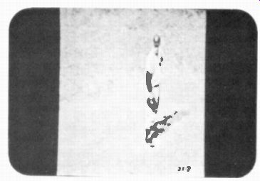
FIGURE 22-31 INSUFFICIENT WIDTH (RCA)
Black vertical lines. These may be at the left or right side. The effect in Fig. 22-35, called "snivets," is caused by radiation of harmonics of the horizontal scanning current to the signal circuits. Rf chokes of 1 to 10 uH or ferrite beads are used in the horizontal amplifier and damper circuits to prevent the snivets.
Thin, straight, black vertical lines at the left can be caused by Barkhausen oscillations in the horizontal output tube radiated to the signal circuits. This stage usually has a 47-11 parasitic suppressor resistor in series with the control grid. Also, the suppressor grid is generally at V for the dual functions of preventing Barkhausen oscillations and reducing snivets.
No high voltage. This is the most common cause of no brightness. Either the high-voltage rectifier is defective or it has no input from the flyback transformer. Remember that the damper must be operating with the amplifier stage, and the oscillator must supply drive.
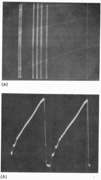
FIGURE 22-32 EXCESSIVE HORIZONTAL DRIVE. (a) THIN WHITE LINES AT LEFT. (b)
RIPPLES IN SCANNING CURRENT.
To localize this trouble, first check to see if the rectifier has high-voltage ac input to its anode. If it does and there is no dc output, the trouble is in the high-voltage rectifier. If there is no flyback high voltage into the rectifier, check the horizontal deflection stages, from the output transformer back to the oscillator.
On the dc output side, the high voltage rectifier tube may be gassy or shorted. Also, disconnect the rectifier lead to the CRT anode to see if the high voltage comes on.
The output stage usually has a fuse, which may be open. A common trouble is a short in the damper, which blows the fuse. See if the output transformer shows burned wires or melted wax.
The resistance of the windings can be checked with an ohmmeter. However, a few shorted turns will not show on the ohmmeter. This trouble can still cause no horizontal output because the short loads down the output circuit. Then the Q is too low for a resonance effect.
To decide whether a short is in the deflection yoke or the flyback transformer, disconnect the yoke. If the boosted B+ voltage goes up, the yoke is bad. If not, the short is in the output transformer.
It should be noted that color receivers often have a focus rectifier and a high-voltage regulator. Trouble in these stages also can result in no brightness on the screen of the picture tube.
FIGURE 22-33 REDUCED WIDTH WITH FOLDOVER AT LEFT CAUSED BY OPEN B+ BOOST
CAPACITOR.

FIGURE 22-34 EXCESSIVE YOKE RINGING
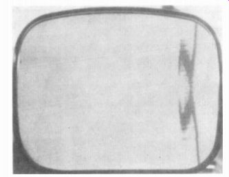
FIGURE 22-35 BLACK "SNIVETS" AT RIGHT.
SUMMARY
1. With tubes the horizontal deflection circuits include the oscillator driving a beam-power amplifier with its diode damper. In addition, the flyback high-voltage supply is in the horizontal output circuit.
2. The oscillator output voltage at 15,750 Hz provides the amplifier grid voltage needed for sawtooth plate current in the output.
3. Autotransformer coupling is generally used from the output stage to the horizontal deflection coils. The amplifier conducts for two-thirds of the cycle to scan the right side of the raster.
4. At the end of trace, the output stage is cut off. Then the output circuit oscillates.
The damper is cut off by the first half-cycle of oscillations, allowing a fast flyback.
5. The high-voltage rectifier conducts during flyback to produce anode voltage for the CRT.
6. Immediately after flyback, the damper conducts. As the damped current decays to zero, the left side of the raster is scanned while the amplifier remains cut off.
Then the output stage starts conducting again to finish the trace.
7. While the damper is conducting, its current charges the B+ boost capacitor. The boosted B+ voltage is the plate supply for the horizontal amplifier tube.
8. The voltage waveshape at all points in the horizontal output circuit is rectangular with sharp flyback pulses. For the usual case of an autotransformer, all taps have positive polarity of flyback pulses. Therefore, the diode damper is inverted, with positive pulses at the cathode for cutoff during flyback but negative deflection voltage for conduction during trace.
9. The frequency of the horizontal scanning current is set by the oscillator and its AFC adjustments. The amplitude adjustments to fill the width of the raster are in the horizontal output. These may include drive, width, and linearity controls.
10. The horizontal amplifier tube operates with grid-leak bias approximately equal to the peak positive drive from the oscillator. A typical bias is -30 to -50 V.
11. A transistor or SCR in the horizontal output stage serves as a switch to supply rectangular voltage for sawtooth current in the inductance of the scanning coils. See Fig. 22-25.
12. In transistorized circuits, a driver stage is used as a buffer between the horizontal oscillator and amplifier. See Fig. 22-26.
13. Insufficient width without distortion indicates a weak horizontal amplifier or low B+ voltage. Reduced width with foldover at the left is caused by trouble in the damper circuit.
14. The most common cause of no brightness is no high voltage. Either the rectifier circuit is defective or there is no horizontal output. Check the horizontal oscillator, amplifier, fuse, damper, flyback transformer and the deflection yoke for no ac input. Check the high voltage rectifier circuit for no dc output.
Sell-Examination (Answers at back of guide)
1. Which stage is not necessary for producing horizontal output: (a) horizontal oscillator; (b) damper; (c) horizontal amplifier; (d) horizontal AFC.
2. The frequency of sawtooth current in the horizontal amplifier is : (a) 60 Hz; (b) 10,500 Hz; (c) 15,750 Hz; (d) 70 kHz.
3. When the horizontal amplifier is conducting peak plate current, the electron scanning beam is at the: (a) left edge of the raster; (b) right edge of the raster; (c) center of trace; (d) center of flyback.
4. Which of the following is conducting during flyback: (a) high-voltage rectifier; (b) output stage; (c) diode damper tube; (d) silicon diode damper.
5. With a resonant frequency of 70 kHz for the horizontal output circuit, the flyback time equals: (a) 5 u-s; (b) 7 u-s; (c) 20 u-s; (d) 50 u-s.
6. With autotransformer coupling, the voltage waveshape at the cathode of the inverted diode damper is: (a) sawtooth; (b) trapezoidal; (c) rectangular with positive flyback pulses; (d) rectangular with negative flyback pulses.
7. With 120 V p-p sawtooth drive at the grid of the horizontal amplifier, its grid-leak bias equals: (a) zero; (b) 10 V; (c) 54 V; (d) 120 V.
8. The voltage induced across a 240-µH inductance by a 5-A current dropping to zero in 8 u-s equals: (a) 80 V; (b) 150 V; (c) 2,000 V; (d) 15,000 V.
9. The B+ boost capacitor charges when the: (a) high-voltage rectifier conducts; (b) beam retraces; (c) damper is cut off; (d) damper is conducting.
10. The damper tube has an open heater. The result is: (a) a wide white bar at the left; (b) thin white bars at the left; (c) foldover at the right; (d) no brightness.
11. For the transistor circuit in Fig. 22-26: (a) Q3 is on for retrace; (b) the scanning coils are in series; (c) Q2 is transformer-coupled to the output stage; (d) the damper D1 is on for retrace.
12. For the SCR circuit in Fig. 22-29: (a) the horizontal oscillator pulses drive the scanning coils; (b) the gate of each SCR is used to turn it off; (c) SCRT is used to produce retrace. (d) SCR,. has B+ of 160 V at the anode.
Essay Questions
1. What three stages in the receiver determine the width of the raster? What stages determine the height? (Low-voltage power supply is not counted.)
2. How is the horizontal oscillator synchronized at 15,750 Hz?
3. Name two types of horizontal oscillator circuits.
4. What is meant by ringing? What two factors determine the ringing frequency?
5. Give six functions of the horizontal output circuit.
6. In horizontal deflection, describe briefly how the scanning current is produced for the right side of trace, the retrace, and the left side of trace.
7. Why is the damper cut off for flyback?
8. What two voltages add to produce the boosted B+ voltage?
9. What three stages must be operating to produce ac input voltage for the high voltage rectifier?
10. Draw the schematic diagram of a horizontal amplifier circuit with autotransformer output. Include the damper and high-voltage rectifier circuits and show boosted B+.
11. Name three circuits that may use boosted B+ as a voltage source.
12. Give two methods of checking with a dc voltmeter to see if the horizontal oscillator is operating.
13. Draw a sine wave of current and of voltage on one graph, showing the two waveforms 90° out of phase. State the main characteristic of the 90° phase difference.
14. Draw one cycle of sawtooth current in the horizontal deflection coils. Mark the trace and retrace periods in microseconds. Indicate which tubes in the output circuit are conducting for three parts of the cycle.
15. Give the function of the circuit in Fig. 22-24.
16. Give the function of the circuit in Fig. 22-30.
17. What is meant by scan rectification for dc supply voltage?
18. Give three differences between horizontal deflection circuits using tubes and those using transistors.
19. Name the three electrodes in an SCR and give the function of each.
20. Describe briefly one method of width control.
21. The fuse Fl in Fig. 22-2 is open. What is the effect on the raster?
22. In Fig. 22-2, give the functions of R _p C _p C2, Cn, C„, and C„.
23. In Fig. 22-28, give the functions of Q8, Q9, Q302, D301, 7 - 4, T _p Fl, the TA301 tripler unit, and the R. potentiometer.
24. From waveshape (c) in Fig. 22-27, for drive voltage on the output transistor, this stage is cut off for what percent of a full cycle?
25. For the table below, indicate which stages are on or off during retrace and any part of trace.
TRACE RETRACE
Horizontal amplifier
High-voltage rectifier
Damper
Problems (Answers to selected problems at back of guide)
1. (a) Calculate the RC time constant of a 0.005-µF coupling capacitor with 1-M-o grid resistance. (b) How much longer than the horizontal scanning period is this time constant? (c) Can grid-leak bias be developed when grid current flows?
2. Approximately how much grid-leak bias is produced for the following peak-to peak values of grid drive: 40 V. 80 V, and 160 V?
3. Referring to Fig. 22-4: (a) What is the average / _p set by the grid bias of -40 V? (b)
What is the E _pI _p plate power dissipation with a 200-V average plate voltage?
4. A power transistor has a 3-A average collector current /(.. The average collector voltage ti c is 10 V. How much is the V ul, power dissipation at the collector?
5. A horizontal output transistor is cut off for retrace and 25 percent of trace.
For how many microseconds is the transistor on?
6. For the horizontal output transformer in Fig. 22-36 below, give the functions for the taps at terminals 1, 2, 3, and 4, with the auxiliary windings L, and L 2.
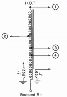
FIGURE 22-36 FOR PROBLEM 6.